
For free samples & the latest literature: https://www.doczj.com/doc/9e9490640.html,, or phone 1-800-998-8800.For small orders, phone 1-800-835-8769.
General Description
The MAX5165 contains four 1-to-8 multiplexers and 32sample/hold amplifiers. A single analog input connects to all four internal 1-to-8 multiplexers. The sample/hold amplifiers are organized into four octal sample/holds with independent TTL/CMOS-compatible track/hold enables for each octal set. Additional 3-bit TTL/CMOS-compatible address logic selects the 1-to-8 multiplexer channel. Clamping diodes on each output allow clamp-ing between two external reference voltages. The MAX5165 is available with an output impedance of 50?, 500?, or 1k ?, allowing output filtering.
The MAX5165 operates with +10V and -5V supplies and a separate +5V digital logic supply. Manufactured with a proprietary BiCMOS process, it provides high accura-cy, fast acquisition time, low droop rate, and a low hold step. The device acquires 8V step input signals to 0.01% accuracy in 2.5μs. Transitions from sample mode to hold mode result in only a 0.5mV error. While in hold mode, the output voltage slowly droops at a rate of 1mV/sec. The MAX5165 is available in a 48-pin TQFP package.
Applications
Automatic Test Equipment (ATE)Industrial Process Controls Arbitrary Function Generators Avionics Equipment
Features
o 32-Channel Sample/Hold o Output Clamping
o 0.01% Accuracy of Acquired Signal o 0.01% Linearity Error o Fast Acquisition Time: 2.5μs o Low Droop Rate: 1mV/sec o Low Hold Step: 0.25mV
o Wide Output Voltage Range: +7V to -4V
MAX5165
32-Channel Sample/Hold Amplifier
with a Single Multiplexed Input
________________________________________________________________Maxim Integrated Products
1
19-1469; Rev 0; 7/99
Pin Configuration
Ordering Information
M A X 5165
32-Channel Sample/Hold Amplifier with a Single Multiplexed Input
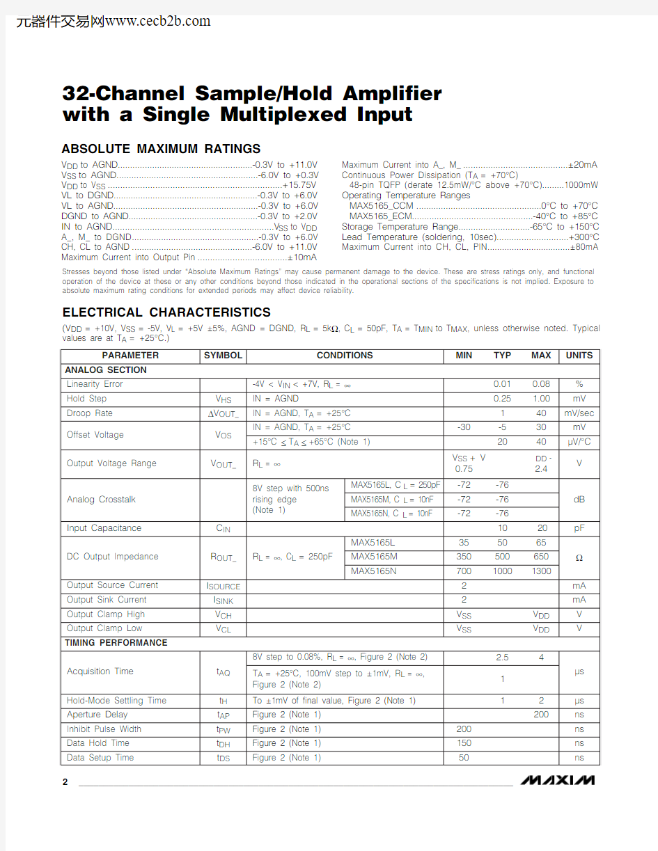
ABSOLUTE MAXIMUM RATINGS
ELECTRICAL CHARACTERISTICS
(V DD = +10V, V SS = -5V, V L = +5V ±5%, AGND = DGND, R L = 5k ?, C L = 50pF, T A = T MIN to T MAX , unless otherwise noted. Typical values are at T A = +25°C.)
Stresses beyond those listed under “Absolute Maximum Ratings” may cause permanent damage to the device. These are stress ratings only, and functional operation of the device at these or any other conditions beyond those indicated in the operational sections of the specifications is not implied. Exposure to absolute maximum rating conditions for extended periods may affect device reliability.
V DD to AGND.......................................................-0.3V to +11.0V V SS to AGND.........................................................-6.0V to +0.3V V DD to V SS ......................................................................+15.75V VL to DGND...........................................................-0.3V to +6.0V VL to AGND...........................................................-0.3V to +6.0V DGND to AGND.....................................................-0.3V to +2.0V IN to AGND.................................................................V SS to V DD A_, M_ to DGND....................................................-0.3V to +6.0V CH, CL to AGND .................................................-6.0V to +11.0V Maximum Current into Output Pin ....................................±10mA
Maximum Current into A_, M_..........................................±20mA Continuous Power Dissipation (T A = +70°C)
48-pin TQFP (derate 12.5mW/°C above +70°C).........1000mW Operating Temperature Ranges
MAX5165_CCM ...................................................0°C to +70°C MAX5165_ECM.................................................-40°C to +85°C Storage Temperature Range.............................-65°C to +150°C Lead Temperature (soldering, 10sec).............................+300°C Maximum Current into CH, CL, PIN..................................±80mA
MAX5165
32-Channel Sample/Hold Amplifier
with a Single Multiplexed Input
_______________________________________________________________________________________3
ELECTRICAL CHARACTERISTICS (continued)
(V DD = +10V, V SS = -5V, V L = +5V ±5%, AGND = DGND, R L = 5k ?, C L = 50pF, T A = T MIN to T MAX , unless otherwise noted. Typical values are at T A = +25°C.)
Note 1:Guaranteed by design.
Note 2:Only one M_ input may be asserted low at a time, so only one channel is selected (see Single vs. Simultaneous Sampling ).Note 3:Do not exceed the absolute maximum rating for V DD to V SS of +15.75V (see Absolute Maximum Ratings ).
M A X 5165
32-Channel Sample/Hold Amplifier with a Single Multiplexed Input 4_______________________________________________________________________________________
Typical Operating Characteristics
(V DD = +10V, V SS = -5V, V L = +5V, IN = GND, R L = ∞, C L = 0, AGND = DGND, V CH = V DD , V CL = V SS , T A = +25°C, unless other-wise noted.)
042108616141218-40
20
-20
40
60
80
100DROOP RATE vs. TEMPERATURE
M A X 5165-01
TEMPERATURE (°C)
D R O O P R A T
E (m V /s e c )
1k
10k
0-10
-20-30-40-60-50-70-80-90
1
10
100POWER-SUPPLY REJECTION RATIO
(HOLD MODE)
FREQUENCY (kHz)
P S R R (d B )
1k
10k
0-10-20-30-40-60-50-70
-80-901
10
100POWER-SUPPLY REJECTION RATIO
(SAMPLE MODE)
FREQUENCY (kHz)
P S R R (d B )
25
50
75-40
20
40
-20
60
80
100
HOLD STEP vs. TEMPERATURE
M A X 5165-04
TEMPERATURE (°C)
H O L D S T E P (μV )
02010
50403060709080
100
-5.0
-3.0
-1.0
1.0
3.0
5.0
7.0
HOLD STEP vs. INPUT VOLTAGE
M A X 5165-07
INPUT VOLTAGE (V)
H O L D S T E P (μV )
-5.0
-4.0-4.5-3.0-3.5-2.5-2.0-40
20
40
-20
60
80
100
OFFSET VOLTAGE vs. TEMPERATURE
M A X 5165-05
TEMPERATURE (°C)
O F F S E T V O L T A G E (m V )
1.00
1.101.051.201.151.301.251.351.451.401.50-5.0-
2.0-0.51.0-
3.5 2.5
4.0
5.58.57.010.0
DROOP RATE vs. INPUT VOLTAGE
M A X 5165-06
INPUT VOLTAGE (V)
D R O O P R A T
E (m V /s e c )-4.5
-4.3-4.4
-4.0-4.1-4.2-3.9-3.8-3.6-3.7-3.5
-5.0
-3.0
-1.0
1.0
3.0
5.0
7.0
OFFSET VOLTAGE vs. INPUT VOLTAGE
M A X 5165-08
INPUT VOLTAGE (V)
O F F S E T V O L T A G E (m V )
MAX5165
32-Channel Sample/Hold Amplifier
with a Single Multiplexed Input
_______________________________________________________________________________________5
Figure 1. Functional Diagram
M A X 5165
32-Channel Sample/Hold Amplifier with a Single Multiplexed Input 6_______________________________________________________________________________________
_______________Detailed Description
The MAX5165 connects a single analog input to the inputs of four internal 1-to-8 analog multiplexers. Each multiplexer channel connects to a buffered sample/hold circuit and a series output resistor, creating a single-input device with 32 sample/hold output channels.Three multiplexer channel-address inputs and four mode-select inputs (one for each multiplexer) control channel selection and sample/hold functions (Figure 1and Tables 1, 2).
Digital Interface
Three address pins and 3-to-8 address decoder logic select the channel for all four internal analog multiplex-ers. The mode-select inputs (M3–M0) independently control the sample/hold functions for each multiplexer (Tables 1, 2).
Sample/Hold
The MAX5165 contains 32 buffered sample/hold cir-cuits with internal hold capacitors. Internal hold capaci-tors minimize leakage current, dielectric absorption,feedthrough, and required board space. The value of the hold capacitor affects acquisition time and droop rate. Lower capacitance allows faster acquisition times but increases the droop rate. Higher values increase hold time and acquisition time. The hold capacitor used in the MAX5165 provides fast 2.5μs (typ) acquisition time while maintaining a low 1mV/sec (typ) droop rate,making the sample/hold ideal for high-speed sampling.
Pin Description
Sample Mode
Driving M3–M0 low (one at a time) selects sample mode (Tables 1, 2). During sample mode, the selected multiplexer channel connects to I N, allowing the hold capacitor to acquire the input signal. To guarantee an accurate sample, maintain sample mode for at least 4μs. The output of the S/H amplifier tracks the input after 4μs. Only the addressed channel on the selected multiplexer samples the input; all other channels remain in hold mode.
Hold Mode
Driving M3–M0 high selects hold mode. Hold mode dis-ables the multiplexer and disconnects all eight chan-nels on the 1-to-8 multiplexer from the input. When a channel is disconnected, the hold capacitor maintains the sampled voltage at the output with a 1mV/sec droop rate (towards V DD ).
Hold Step
When switching between sample mode and hold mode,the voltage of the hold capacitor changes due to charge injection from stray capacitance. This voltage change, called hold step, is minimized by limiting the amount of stray capacitance seen by the hold capaci-tor. The MAX5165 limits the hold step to 0.25mV (typ).An output capacitor to ground can be used to filter out this small hold-step error.
Output
The MAX5165 contains an output buffer for each multi-plexer channel (32 total), so the hold capacitor sees a high-impedance input, reducing the droop rate. The capacitor droops at a 1mV/sec (typ) rate while in hold mode. The buffer also provides a low output imped-ance; however, the device contains output resistors in series with the buffer output (Figure 1) for selected out-put filtering. To provide greater design flexibility, the MAX5165 is available with an R O of 50?, 500?, or 1k ?.N ote: Output loads increase the analog supply cur-rent (I DD and I SS ).Excessive loading of the output(s)damages the device by consuming more power than the device will dissipate (see Absolute Maximum Ratings ).The resistor-divider formed by the output resistor (R OUT )and load impedance (R L ) scales the sampled voltage (V SAMP ). Determine the output voltage (V OUT_) as follows:
Voltage Gain = A V = R L / (R L + R OUT )
V OUT_= V SAMP ·A V
The maximum output voltage range depends on the analog supply voltages available, and the scaling factor used:
(V SS + 0.75V) ·A V ≤V OUT_≤(V DD - 2.4V) ·A V when R L = ∞, then A V = 1 and this equation becomes:
(V SS + 0.75V) ≤V OUT ≤(V DD - 2.4V)
MAX5165
32-Channel Sample/Hold Amplifier
with a Single Multiplexed Input
_______________________________________________________________________________________
7
Table 1. Output Selection
0 = Logic Low, 1 = Logic High
0 = Logic Low, 1 = Logic High
* Only one M_ input asserted low; all others must be logic high to meet the timing specification (see Single vs. Simultaneous Sampling section).
M A X 5165
Output Clamp
The MAX5165 clamps the output between two external-ly applied reference voltages. I nternal diodes connect all outputs to the clamping voltages, restricting the out-put voltage to:
V CH + 0.7V ≤V OUT_≤V CL - 0.7V When the clamping voltage exceeds the maximum out-put voltage, the maximum output voltage will be the lim-iting factor. To disable output clamping, connect CH to V DD and C L to V SS to set the clamping voltages beyond the maximum output voltage range. The clamping diodes allow the MAX5165 to be used with other devices requiring restricted input voltages.
Timing Definitions
Acquisition time (t AQ ) is the amount of time the MAX5165 must remain in sample mode for the hold capacitor to acquire an accurate sample. The hold-mode settling time (t H ) is the amount of time necessary for the output voltage to settle to its final value. Aperture delay (t AP ) is the time interval required to disconnect the input from the hold capacitor. The inhibit pulse width (t PW ) is the amount of time the MAX5165 must remain in hold mode while the address is changed. The data setup time (t DS ) is the amount of time an address must be maintained before the address becomes valid.The data hold time (t DH ) is the amount of time that an address must be maintained after mode select has gone from low to high (Figure 2).
__________Applications Information
Control-Line Reduction
The MAX5165 contains four separate 1-to-8 multiplex-ers and individual mode selectors for each multiplexer.Configure the device to sample only one channel at a time or up to four channels (with the same address, see Table 1) simultaneously. When sampling one channel at a time, use an external 2-to-4 decoder (with active-low outputs) to reduce the number of digital control lines from seven to five (Figure 3).
Single vs. Simultaneous Sampling
I ndividually control the four mode/multiplexer-select pins to simultaneously sample on four channels, the same channel for each multiplexer (Figure 4). Each mode-select pin controls sampling on one of the 1-to-8multiplexers, while the 3-bit address selects one of the eight channels on all the multiplexers (Tables 1, 2).Setting any combination of the mode-select pins low enables sampling on the addressed channels for the selected multiplexers.
Simultaneously sampling two or more channels reduces offset voltage but increases acquisition time. Multiply the single-channel acquisition time by the number of channels sampling.
32-Channel Sample/Hold Amplifier with a Single Multiplexed Input 8
_______________________________________________________________________________________
Figure 2. Timing Performance
MAX5165
32-Channel Sample/Hold Amplifier
with a Single Multiplexed Input
_______________________________________________________________________________________
9
Figure 3. Control-Line Reduction
Figure 4. Simultaneous Sampling
M A X 5165
32-Channel Sample/Hold Amplifier with a Single Multiplexed Input 10______________________________________________________________________________________
Figure 5. Multiplexing a DAC
Chip Information
TRANSISTOR COUNT: 5077
Multiplexed DAC
Figure 5 shows a typical demultiplexer application.Different digital codes are converted by the digital-to-analog converter (DAC) and then stored on 32 different channels of the MAX5165. The 100mV/sec (max) droop rate requires refreshing the hold capacitors every 100ms before the voltage drops by 1/2LSB for an 8-bit DAC with a 5V full-scale voltage.
Powering the MAX5165
The MAX5165 does not require a special power-up sequence to avoid latchup. The device requires three separate supply voltages for operation; however, when one or two of the voltages are not available, DC-DC charge-pump (switched-capacitor) converters provide a simple, efficient solution. The MAX860 provides volt-age doubling or inversion, ideal for conversions from +5V to +10V or from +5V to -5V. The MAX860 also functions as a voltage divider to provide conversion from +10V to +5V.
MAX5165
32-Channel Sample/Hold Amplifier
with a Single Multiplexed Input
______________________________________________________________________________________11
Package Information
M A X 5165
32-Channel Sample/Hold Amplifier with a Single Multiplexed Input Maxim cannot assume responsibility for use of any circuitry other than circuitry entirely embodied in a Maxim product. No circuit patent licenses are implied. Maxim reserves the right to change the circuitry and specifications without notice at any time.
12____________________Maxim Integrated Products, 120 San Gabriel Drive, Sunnyvale, CA 94086 408-737-7600?1999 Maxim Integrated Products
Printed USA
is a registered trademark of Maxim Integrated Products.
NOTES