TC1303B
Features
?Dual-Output Regulator (500mA Buck Regulator and 300mA Low-Dropout Regulator)
?Power-Good Output with 300ms Delay
?Total Device Quiescent Current = 65μA, Typ.?Independent Shutdown for Buck and LDO Outputs
?Both Outputs Internally Compensated ?Synchronous Buck Regulator:
-Over 90% Typical Efficiency
- 2.0MHz Fixed Frequency PWM
(Heavy Load)
-Low Output Noise
-Automatic PWM to PFM mode transition
-Adjustable (0.8V to 4.5V) and Standard Fixed
Output Voltages (0.8V, 1.2V, 1.5V, 1.8V, 2.5V,
3.3V)
?Low-Dropout Regulator:
-Low-Dropout Voltage=137mV Typ. @
200mA
-Standard Fixed Output Voltages
(1.5V, 1.8V, 2.5V, 3.3V)
?Power-Good Function:
-Monitors LDO Output Function (TC1303B)
-300ms Delay Used for Processor Reset ?Small 10-pin 3X3 DFN or MSOP Package Options
?Operating Junction Temperature Range:
--40°C to +125°C
?Undervoltage Lockout (UVLO)
?Output Short Circuit Protection ?Overtemperature Protection
Applications
?Cellular Phones
?Portable Computers
?USB Powered Devices
?Handheld Medical Instruments
?Organizers and PDAs Description
The TC1303B combines a 500mA synchronous buck regulator and 300mA Low-Dropout Regulator (LDO) with a power-good monitor to provide a highly integrated solution for devices that require multiple supply voltages. The unique combination of an integrated buck switching regulator and low-dropout linear regulator provides the lowest system cost for dual-output voltage applications that require one lower processor core voltage and one higher bias voltage. The 500mA synchronous buck regulator switches at a fixed frequency of 2.0MHz when the load is heavy providing a low noise, small-size solution. When the load on the buck output is reduced to light levels, it changes operation to a Pulse Frequency Modulation (PFM) mode to minimize quiescent current draw from the battery. No intervention is necessary for smooth transition from one mode to another.
The LDO provides a 300mA auxiliary output that requires a single 1μF ceramic output capacitor, minimizing board area and cost. The typical dropout voltage for the LDO output is 137mV for a 200mA load.
For the TC1303B, the power-good output logic level is based on the regulation of the LDO output only. The buck regulator can be turned on and off without affecting the power-good signal.
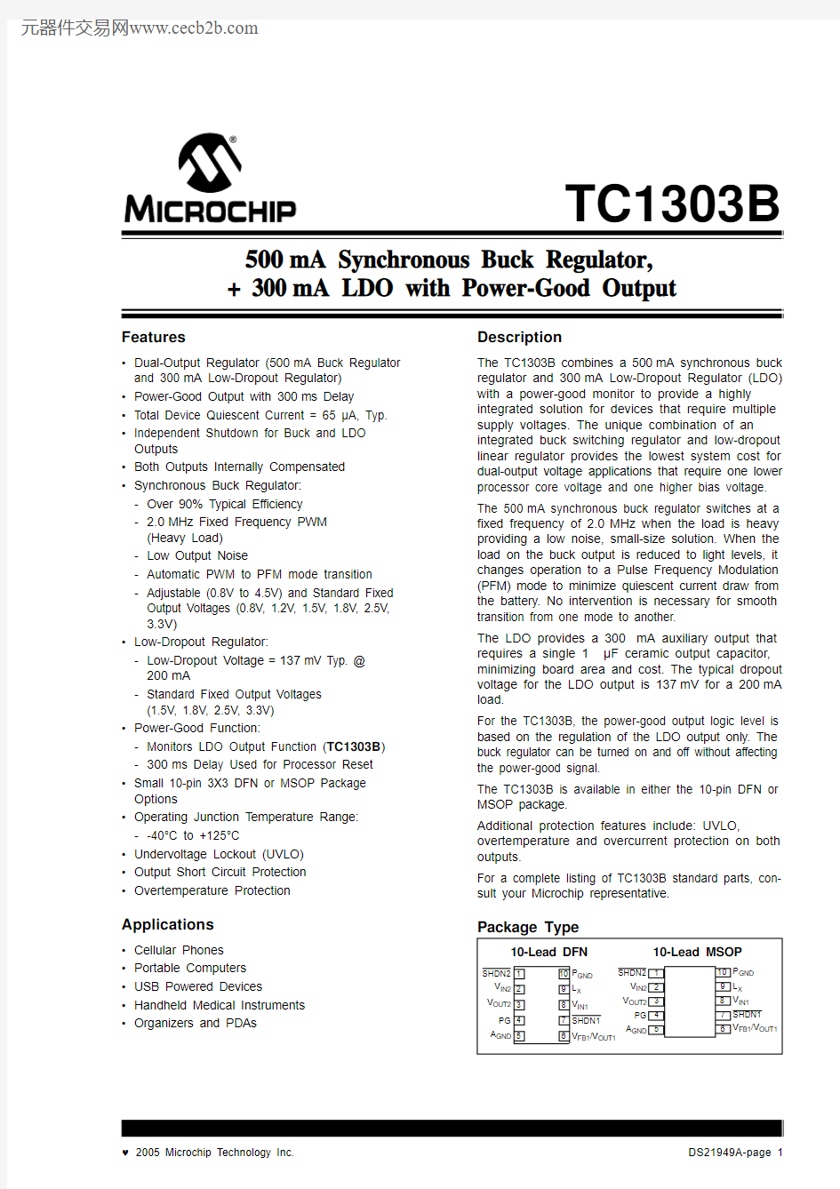
The TC1303B is available in either the 10-pin DFN or MSOP package.
Additional protection features include: UVLO, overtemperature and overcurrent protection on both outputs.
For a complete listing of TC1303B standard parts, con-sult your Microchip representative.
Package Type
10-Lead DFN
1
2
6
8
7
9
10
5
4
3
SHDN2
V IN2
V OUT2
A GND
P GND
L X
V IN1
SHDN1
V FB1/V OUT1
PG
10-Lead MSOP
1
2
6
8
7
9
10
5
4
3
SHDN2
V IN2
V OUT2
A GND
P GND
L X
V IN1
SHDN1
V FB1/V OUT1
PG
500mA Synchronous Buck Regulator,
+ 300mA LDO with Power-Good Output
? 2005 Microchip Technology Inc.DS21949A-page 1
TC1303B
DS21949A-page 2? 2005 Microchip Technology Inc.
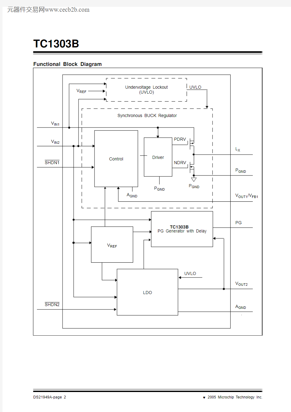
Functional Block Diagram
Synchronous BUCK Regulator
NDRV
PDRV
P GND
V IN1
L X
Driver
P GND
Control
V OUT1/V FB1
V IN2
SHDN1
PG
V REF
LDO
V OUT2
A GND
A GND
P GND
Undervoltage Lockout
UVLO
UVLO
SHDN2
V REF
TC1303B
PG Generator with Delay
(UVLO)
? 2005 Microchip Technology Inc.DS21949A-page 3
TC1303B
Typical Application Circuits
10-Lead DFN
1268
79
1054
3SHDN2V IN2V OUT2A GND
P GND L X
V IN1SHDN1V OUT1PG
4.7μF
Processor RESET
Input Voltage 4.7μH
4.7μF
2.1V @1μF
3.3V @
4.5V to
5.5V Adjustable Output Application
121k Ω
200k Ω 4.99k Ω33pF 126879
10
5
4
3SHDN2V IN2V OUT2A GND
P GND L X V IN1SHDN1V OUT1PG
4.7μF
Processor RESET
4.7μH
4.7μF
1.5V @ 500mA
1μF
2.5V @ 300mA
2.7V to 4.2V
TC1303B
V OUT1
V OUT2
V IN V OUT1V OUT2
1.0μF
*Optional Capacitor V IN2
300mA
500mA
Note: Connect DFN package exposed pad to A GND .
10-Lead MSOP
Fixed Output Application
TC1303B
Note
TC1303B
DS21949A-page 4? 2005 Microchip Technology Inc.
1.0
ELECTRICAL
CHARACTERISTICS
Absolute Maximum Ratings ?
V IN - A GND ......................................................................6.0V All Other I/O ..............................(A GND - 0.3V) to (V IN + 0.3V)L X to P GND ..............................................-0.3V to (V IN + 0.3V)P GND to A GND ...................................................-0.3V to +0.3V Output Short Circuit Current .................................Continuous Power Dissipation (Note 7)..........................Internally Limited Storage temperature.....................................-65°C to +150°C Ambient Temp. with Power Applied.................-40°C to +85°C Operating Junction Temperature...................-40°C to +125°C ESD protection on all pins (HBM)....................................... 3kV
? Notice: Stresses above those listed under “Maximum Ratings” may cause permanent damage to the device. This is a stress rating only and functional operation of the device at those or any other conditions above those indicated in the operational listings of this specification is not implied.Exposure to maximum rating conditions for extended periods may affect device reliability.
DC CHARACTERISTICS
Electrical Characteristics: V IN1=V IN2=SHDN1,2=3.6V,C OUT1=C IN =4.7μF, C OUT2=1μF,L =4.7μH, V OUT1 (ADJ)=1.8V, I OUT1=100ma, I OUT2=0.1mA T A =+25°C. Boldface specifications apply over the T A range of -40°C to +85°C .
Parameters
Sym
Min
Typ
Max
Units
Conditions
Input/Output Characteristics Input Voltage
V IN 2.7— 5.5V Note 1, Note 2, Note 8Maximum Output Current I OUT1_MAX 500——mA Note 1Maximum Output Current I OUT2_MAX 300——mA Note 1
Shutdown Current
Combined V IN1 and V IN2 Current I IN_SHDN
—0.051μA SHDN1=SHDN2=GND TC1303B Operating I Q I Q
—65.0110μA SHDN1=SHDN2=V IN2I OUT1=0mA,I OUT2=0mA Synchronous Buck I Q —38—μA SHDN1 = V IN , SHDN2 = GND LDO I Q + Voltage Monitor I Q —46—μA SHDN1 = GND, SHDN2 = V IN2Shutdown/UVLO/Thermal Shutdown Characteristics
SHDN1,SHDN2,
Logic Input Voltage Low V IL ——15%V IN V IN1=V IN2=2.7V to 5.5V SHDN1,SHDN2,
Logic Input Voltage High V IH 45——%V IN V IN1=V IN2=2.7V to 5.5V SHDN1,SHDN2,
Input Leakage Current I IN -1.0
±0.01
1.0
μA
V IN1=V IN2=2.7V to 5.5V SHDNX =GND SHDNY =V IN Thermal Shutdown
T SHD —165—°C Note 6, Note 7Thermal Shutdown Hysteresis T SHD-HYS —10—°C Undervoltage Lockout (V OUT1 and V OUT2)
UVLO 2.4 2.55 2.7V V IN1 Falling
Undervoltage Lockout Hysteresis UVLO -HYS
—
200
—
mV
Note 1:
The Minimum V IN has to meet two conditions: V IN ≥ 2.7V and V IN ≥ V RX + V DROPOUT , V RX = V R1 or V R2.2:V RX is the regulator output voltage setting.
3:TCV OUT2 = ((V OUT2max – V OUT2min ) * 106)/(V OUT2 * D T ).
4:
Regulation is measured at a constant junction temperature using low duty cycle pulse testing. Load regulation is tested over a load range from 0.1mA to the maximum specified output current.
5:Dropout voltage is defined as the input to output voltage differential at which the output voltage drops 2% below its nominal value measured at a 1V differential.
6:
The maximum allowable power dissipation is a function of ambient temperature, the maximum allowable junction
temperature and the thermal resistance from junction to air. (i.e. T A , T J , θJA ). Exceeding the maximum allowable power dissipation causes the device to initiate thermal shutdown.
7:
The integrated MOSFET switches have an integral diode from the L X pin to V IN , and from L X to P GND . In cases where these diodes are forward-biased, the package power dissipation limits must be adhered to. Thermal protection is not able to limit the junction temperature for these cases.8:
V IN1 and V IN2 are supplied by the same input source.
TC1303B
Synchronous Buck Regulator (V OUT1)
Adjustable Output Voltage Range V OUT10.8— 4.5V
Adjustable Reference Feedback
Voltage (V FB1)
V FB10.780.80.82V
Feedback Input Bias Current
(I FB1)
I VFB1—-1.5—nA
Output Voltage Tolerance Fixed
(V OUT1)
V OUT1-2.5±0.3+2.5%Note2
Line Regulation (V OUT1)V LINE-REG—0.2—%/V V IN =V R+1V to 5.5V,
I LOAD = 100mA
Load Regulation (V OUT1)V LOAD-REG—0.2—%V IN=V R+1.5V,I LOAD=100mA to
500mA (Note1)
Dropout Voltage V OUT1V IN – V OUT1—280—mV I OUT1 = 500mA, V OUT1=3.3V
(Note5)
Internal Oscillator Frequency F OSC 1.6 2.0 2.4MHz
Start Up Time T SS—0.5—ms T R = 10% to 90%
R DSon P-CHANNEL R DSon-P—450650mΩI P=100mA
R DSon N-CHANNEL R DSon-N—450650mΩI N=100mA
L X Pin Leakage Current I LX-1.0±0.01 1.0μA SHDN = 0V, V IN = 5.5V, L X = 0V,
L X = 5.5V
Positive Current Limit Threshold+I LX(MAX)—700—mA
LDO Output (V OUT2)
Output Voltage Tolerance (V OUT2)V OUT2-2.5±0.3+2.5%Note2
Temperature Coefficient TCV OUT—25—ppm/°C Note3
Line RegulationΔV OUT2/
ΔV IN
-0.2±0.02+0.2%/V(V R+1V) ≤ V IN≤ 5.5V
Load Regulation, V OUT2≥ 2.5VΔV OUT2/
I OUT2
-0.750.1+0.75%I OUT2 = 0.1mA to 300mA(Note4)
Load Regulation, V OUT2 < 2.5VΔV OUT2/
I OUT2
-0.900.1+0.90%I OUT2 = 0.1mA to 300mA(Note4)
Dropout Voltage V OUT2 > 2.5V V IN – V OUT2—137
205300
500
mV I OUT2 = 200mA (Note5)
I OUT2=300mA
Power Supply Rejection Ratio PSRR—62—dB f ≤ 100Hz, I OUT1 = I OUT2 = 50mA,
C IN = 0μF
Output Noise eN— 1.8—μV/(Hz)? f ≤ 1kHz, I OUT2=50mA,
SHDN1=GND
Output Short Circuit Current (Average)I OUT sc2—240—mA R LOAD2≤ 1Ω
DC CHARACTERISTICS (CONTINUED)
Electrical Characteristics: V IN1=V IN2=SHDN1,2=3.6V,C OUT1=C IN=4.7μF, C OUT2=1μF,L=4.7μH, V OUT1 (ADJ)=1.8V,
I OUT1=100ma, I OUT2=0.1mA T A=+25°C. Boldface specifications apply over the T A range of -40°C to +85°C.
Parameters Sym Min Typ Max Units Conditions
Note1:The Minimum V IN has to meet two conditions: V IN≥ 2.7V and V IN≥ V RX + V DROPOUT, V RX = V R1 or V R2.
2:V RX is the regulator output voltage setting.
3:TCV OUT2 = ((V OUT2max – V OUT2min) * 106)/(V OUT2 * D T).
4:Regulation is measured at a constant junction temperature using low duty cycle pulse testing. Load regulation is tested over a load range from 0.1mA to the maximum specified output current.
5:Dropout voltage is defined as the input to output voltage differential at which the output voltage drops 2% below its nominal value measured at a 1V differential.
6:The maximum allowable power dissipation is a function of ambient temperature, the maximum allowable junction temperature and the thermal resistance from junction to air. (i.e. T A, T J, θJA). Exceeding the maximum allowable power
dissipation causes the device to initiate thermal shutdown.
7:The integrated MOSFET switches have an integral diode from the L X pin to V IN, and from L X to P GND. In cases where these diodes are forward-biased, the package power dissipation limits must be adhered to. Thermal protection is not
able to limit the junction temperature for these cases.
8:V IN1 and V IN2 are supplied by the same input source.
? 2005 Microchip Technology Inc.DS21949A-page 5
TC1303B
DS21949A-page 6? 2005 Microchip Technology Inc.
Wake-Up Time (From SHDN2 mode), (V OUT2)
t WK —31100μs I OUT1 = I OUT2 = 50mA Settling Time (From SHDN2 mode), (V OUT2)t S
—
100
—
μs
I OUT1 = I OUT2 = 50mA
Power-Good Voltage Range PG
V PG
1.01.2—
5.55.5V
T A = 0°C to +70°C T A = -40°C to +85°C V IN ≤ 2.7 I SINK = 100μA PG Threshold High (V OUT1 or V OUT2)V TH_H —9496% of V OUTX On Rising V OUT1 or V OUT2V OUTX =V OUT1 or V OUT2PG Threshold Low (V OUT1 or V OUT2)V TH_L 8992—% of V OUTX On Falling V OUT1 or V OUT2V OUTX =V OUT1 or V OUT2PG Threshold Hysteresis (V OUT1 and V OUT2)V TH_HYS —2—
% of V OUTX
V OUTX =V OUT1 or V OUT2
PG Threshold Tempco ΔV TH /ΔT —30—ppm/°C PG Delay
t RPD —165—μs V OUT1 or V OUT2=(V TH + 100mV)
to (V TH - 100mV)
PG Active Time-out Period
t RPU
140
262
560
ms
V OUT1or V OUT2=V TH -100mV to V TH +100mV,I SINK = 1.2mA
PG Output Voltage Low
PG_V OL
——0.2V
V OUT1o r V OUT2=V TH -100mV , I PG = 1.2mA V IN2>2.7V
I PG = 100μA, 1.0V PG_V OH 0.9*V OUT2 ——V V OUT1 or V OUT2=V TH + 100mV V OUT2 ≥ 1.8V, I PG =-500μA V OUT2 < 1.8V,I PG =-300μA DC CHARACTERISTICS (CONTINUED) Electrical Characteristics: V IN1=V IN2=SHDN1,2=3.6V,C OUT1=C IN =4.7μF, C OUT2=1μF,L =4.7μH, V OUT1 (ADJ)=1.8V, I OUT1=100ma, I OUT2=0.1mA T A =+25°C. Boldface specifications apply over the T A range of -40°C to +85°C . Parameters Sym Min Typ Max Units Conditions Note 1: The Minimum V IN has to meet two conditions: V IN ≥ 2.7V and V IN ≥ V RX + V DROPOUT , V RX = V R1 or V R2.2:V RX is the regulator output voltage setting. 3:TCV OUT2 = ((V OUT2max – V OUT2min ) * 106)/(V OUT2 * D T ). 4: Regulation is measured at a constant junction temperature using low duty cycle pulse testing. Load regulation is tested over a load range from 0.1mA to the maximum specified output current. 5:Dropout voltage is defined as the input to output voltage differential at which the output voltage drops 2% below its nominal value measured at a 1V differential. 6: The maximum allowable power dissipation is a function of ambient temperature, the maximum allowable junction temperature and the thermal resistance from junction to air. (i.e. T A , T J , θJA ). Exceeding the maximum allowable power dissipation causes the device to initiate thermal shutdown. 7: The integrated MOSFET switches have an integral diode from the L X pin to V IN , and from L X to P GND . In cases where these diodes are forward-biased, the package power dissipation limits must be adhered to. Thermal protection is not able to limit the junction temperature for these cases.8: V IN1 and V IN2 are supplied by the same input source. TC1303B TEMPERATURE SPECIFICATIONS Electrical Specifications: Unless otherwise indicated, all limits are specified for: V IN = +2.7V to +5.5V Parameters Sym Min Typ Max Units Conditions Temperature Ranges T J-40—+125°C Steady state Operating Junction Temperature Range Storage Temperature Range T A-65—+150°C Maximum Junction Temperature T J——+150°C Transient Thermal Package Resistances Thermal Resistance, 10L-DFNθJA—41—°C/W Typical 4-layer board with Internal Ground Plane and 2 Vias in Thermal Pad Thermal Resistance, 10L-MSOPθJA—113—°C/W Typical 4-layer board with Internal Ground Plane ? 2005 Microchip Technology Inc.DS21949A-page 7 TC1303B DS21949A-page 8? 2005 Microchip Technology Inc. 2.0 TYPICAL PERFORMANCE CURVES Note: Unless otherwise indicated, V IN1= V IN2=SHDN1,2=3.6V,C OUT1=C IN =4.7μF, C OUT2=1μF,L =4.7μH, V OUT1 (ADJ)=1.8V, T A =+25°C. Boldface specifications apply over the T A range of -40°C to +85°C. T A =+25°C. Adjustable or fixed output voltage options can be used to generate the Typical Performance Characteristics. FIGURE 2-1:I Q Switcher and LDO Current vs. Ambient Temperature. FIGURE 2-2:I Q Switcher Current vs. Ambient Temperature. FIGURE 2-3:I Q LDO Current vs. Ambient Temperature. FIGURE 2-4:V OUT1 Output Efficiency vs. Input Voltage (V OUT1 = 1.2V). FIGURE 2-5:V OUT1 Output Efficiency vs. I OUT1 (V OUT1 = 1.2V). FIGURE 2-6:V OUT1 Output Efficiency vs. Input Voltage (V OUT1 = 1.8V). Note: The graphs and tables provided following this note are a statistical summary based on a limited number of samples and are provided for informational purposes only. The performance characteristics listed herein are not tested or guaranteed. In some graphs or tables, the data presented may be outside the specified operating range (e.g., outside specified power supply range) and therefore outside the warranted range. TC1303B Note: Unless otherwise indicated, V IN1= V IN2=SHDN1,2 =3.6V, C OUT1=C IN=4.7μF, C OUT2=1μF,L=4.7μH, V OUT1 (ADJ)=1.8V, T A=+25°C. Boldface specifications apply over the T A range of -40°C to +85°C. T A=+25°C. Adjustable or fixed output voltage options can be used to generate the Typical Performance Characteristics. FIGURE 2-7:V OUT1 Output Efficiency vs. I OUT1 (V OUT1 = 1.8V). FIGURE 2-8:V OUT1 Output Efficiency vs. Input Voltage (V OUT1 = 3.3V). FIGURE 2-9:V OUT1 Output Efficiency vs. I OUT1 (V OUT1 = 3.3V). FIGURE 2-10:V OUT1 vs. I OUT1 (V OUT1 = 1.2V). FIGURE 2-11:V OUT1 vs. I OUT1 (V OUT1 = 1.8V). FIGURE 2-12:V OUT1 vs. I OUT1 (V OUT1 = 3.3V). ? 2005 Microchip Technology Inc.DS21949A-page 9 TC1303B DS21949A-page 10 2005 Microchip Technology Inc. Note: Unless otherwise indicated, V IN1= V IN2=SHDN1,2 =3.6V, C OUT1=C IN =4.7μF, C OUT2=1μF, L =4.7μH, V OUT1 (ADJ)=1.8V, T A =+25°C. Boldface specifications apply over the T A range of -40°C to +85°C. T A =+25°C. Adjustable or fixed output voltage options can be used to generate the Typical Performance Characteristics. OUT1 Switching Frequency vs. Input Voltage. OUT1 Switching Frequency vs. Ambient Temperature. OUT1 Adjustable Feedback Voltage vs. Ambient Temperature. OUT1 Switch Resistance vs. Input Voltage. Resistance vs. Ambient Temperature. OUT1 Dropout Voltage vs. Ambient Temperature. TC1303B Note: Unless otherwise indicated, V IN1= V IN2=SHDN1,2 =3.6V, C OUT1=C IN=4.7μF, C OUT2=1μF,L=4.7μH, V OUT1 (ADJ)=1.8V, T A=+25°C. Boldface specifications apply over the T A range of -40°C to +85°C. T A=+25°C. Adjustable or fixed output voltage options can be used to generate the Typical Performance Characteristics. FIGURE 2-19:V OUT1 and V OUT2 Heavy Load Switching Waveforms vs. Time. FIGURE 2-20:V OUT1 and V OUT2 Light Load Switching Waveforms vs. Time. FIGURE 2-21:V OUT2 Output Voltage vs. Input Voltage (V OUT2 = 1.5V). FIGURE 2-22:V OUT2 Output Voltage vs. Input Voltage (V OUT2 = 1.8V). FIGURE 2-23:V OUT2 Output Voltage vs. Input Voltage (V OUT2 = 2.5V). FIGURE 2-24:V OUT2 Output Voltage vs. Input Voltage (V OUT2 = 3.3V). ? 2005 Microchip Technology Inc.DS21949A-page 11 TC1303B DS21949A-page 12? 2005 Microchip Technology Inc. Note: Unless otherwise indicated, V IN1= V IN2=SHDN1,2 =3.6V, C OUT1=C IN =4.7μF, C OUT2=1μF,L =4.7μH, V OUT1 (ADJ)=1.8V, T A =+25°C. Boldface specifications apply over the T A range of -40°C to +85°C. T A =+25°C. Adjustable or fixed output voltage options can be used to generate the Typical Performance Characteristics. FIGURE 2-25:V OUT2 Dropout Voltage vs. Ambient Temperature (V OUT2 = 2.5V). FIGURE 2-26:V OUT2 Dropout Voltage vs. Ambient Temperature (V OUT2 = 3.3V). FIGURE 2-27:V OUT2 Line Regulation vs. Ambient Temperature.FIGURE 2-28:V OUT2 Load Regulation vs. Ambient Temperature. FIGURE 2-29:PG Active Delay Time-out vs. Ambient Temperature. FIGURE 2-30:PG Threshold Voltage vs. Ambient Temperature. TC1303B Note: Unless otherwise indicated, V IN1= V IN2=SHDN1,2 =3.6V, C OUT1=C IN=4.7μF, C OUT2 =1μF,L=4.7μH, V OUT1 (ADJ)=1.8V, T A=+25°C. Boldface specifications apply over the T A range of -40°C to +85°C. T A=+25°C. Adjustable or fixed output voltage options can be used to generate the Typical Performance Characteristics. FIGURE 2-31:PG Output Voltage Level Low vs. Ambient Temperature. FIGURE 2-32:PG Output Voltage Level High vs. Ambient Temperature. FIGURE 2-33:V OUT2 Power Supply Ripple Rejection vs. Frequency. FIGURE 2-34:V OUT2 Noise vs. Frequency. FIGURE 2-35:V OUT1 Load Step Response vs. Time. FIGURE 2-36:V OUT2 Load Step Response vs. Time. ? 2005 Microchip Technology Inc.DS21949A-page 13 TC1303B DS21949A-page 14? 2005 Microchip Technology Inc. Note: Unless otherwise indicated, V IN1= V IN2=SHDN1,2 =3.6V, C OUT1=C IN =4.7μF, C OUT2=1μF,L =4.7μH, V OUT1 (ADJ)=1.8V, T A =+25°C. Boldface specifications apply over the T A range of -40°C to +85°C. T A =+25°C. Adjustable or fixed output voltage options can be used to generate the Typical Performance Characteristics. FIGURE 2-37:V OUT1 and V OUT2 Line Step Response vs. Time.FIGURE 2-38:V OUT1 and V OUT2 Startup Waveforms. FIGURE 2-39:V OUT1 and V OUT2 Shutdown Waveforms. FIGURE 2-40:Power-Good Output Timing. TC1303B 3.0PIN DESCRIPTIONS The descriptions of the pins are listed in Table3-1. TABLE 3-1:PIN FUNCTION TABLE 3.1LDO Shutdown Input Pin (SHDN2) SHDN2 is a logic level input used to turn the LDO Reg-ulator on and off. A logic high (> 45% of V IN), will enable the regulator output. A logic low (< 15% of V IN) will ensure that the output is turned off. 3.2LDO Input Voltage Pin (V IN2) V IN2 is a LDO power input supply pin. Connect variable input voltage source to V IN2. Connect V IN1 and V IN2 together with board traces as short as possible. V IN2 provides the input voltage for the LDO regulator. An additional capacitor can be added to lower the LDO regulator input ripple voltage. 3.3LDO Output Voltage Pin (V OUT2) V OUT2 is a regulated LDO output voltage pin. Connect a 1μF or larger capacitor to V OUT2 and A GND for proper operation. 3.4Power-Good Output Pin (PG) PG is an output level indicating that V OUT2 (LDO) is within 94% of regulation. The PG output is configured as a push-pull for the TC1303B. 3.5Analog Ground Pin (A GND) A GND is the analog ground connection. Tie A GND to the analog portion of the ground plane (A GND). See the physical layout information in Section 5.0 “Application Circuits/Issues” for grounding recommendations. 3.6Buck Regulator Output Sense Pin (V FB/V OUT1) For V OUT1 adjustable output voltage options, connect the center of the output voltage divider to the V FB pin. For fixed-output voltage options, connect the output of the buck regulator to this pin (V OUT1). 3.7Buck Regulator Shutdown Input Pin (SHDN1) regulator on and off. A logic-high (> 45% of V IN), will enable the regulator output. A logic-low (< 15% of V IN) will ensure that the output is turned off. 3.8Buck Regulator Input Voltage Pin (V IN1) V IN1 is the buck regulator power input supply pin. Connect a variable input voltage source to V IN1. Connect V IN1 and V IN2 together with board traces as short as possible. 3.9Buck Inductor Output Pin (L X) Connect L X directly to the buck inductor. This pin carries large signal-level current; all connections should be made as short as possible. 3.10Power Ground Pin (P GND) Connect all large-signal level ground returns to P GND. These large-signal, level ground traces should have a small loop area and length to prevent coupling of switching noise to sensitive traces. Please see the physical layout information supplied in Section 5.0“Application Circuits/Issues” for grounding recommendations. 3.11Exposed Pad (EP) For the DFN package, connect the EP to A GND with vias into the A GND plane. Pin https://www.doczj.com/doc/946977001.html, Function 1SHDN2Active Low Shutdown Input for LDO Output Pin 2V IN2Analog Input Supply Voltage Pin 3V OUT2LDO Output Voltage Pin 4PG Power-good Output Pin 5A GND Analog Ground Pin 6V FB / V OUT1Buck Feedback Voltage (Adjustable Version) / Buck Output Voltage (Fixed Version) Pin 7SHDN1Active Low Shutdown Input for Buck Regulator Output Pin 8V IN1Buck Regulator Input Voltage Pin 9L X Buck Inductor Output Pin 10P GND Power Ground Pin EP Exposed Pad For the DFN package, the center exposed pad is a thermal path to remove heat from the device. Electrically this pad is at ground potential and should be connected to A GND. ? 2005 Microchip Technology Inc.DS21949A-page 15 TC1303B DS21949A-page 16? 2005 Microchip Technology Inc. 4.0 DETAILED DESCRIPTION 4.1 Device Overview The TC1303B combines a 500mA synchronous buck regulator with a 300mA LDO and a power-good output.This unique combination provides a tiny, low-cost solution for applications that require two or more voltage rails. The buck regulator can deliver high-output current over a wide range of input-to-output voltage ratios while maintaining high efficiency. This is typically used for the lower-voltage, high-current processor core. The LDO is a minimal parts-count solution, (single-output capacitor), providing a regulated voltage for an auxiliary rail. The typical LDO dropout voltage (137mV @ 200mA) allows the use of very low input-to-output LDO differential voltages,minimizing the power loss internal to the LDO pass transistor. A power-good output is provided, indicating that the LDO output is in regulation (TC1303B).Additional features include independent shutdown inputs, UVLO, overcurrent and overtemperature shutdown. 4.2Synchronous Buck Regulator The synchronous buck regulator is capable of supply-ing a 500mA continuous output current over a wide range of input and output voltages. The output voltage range is from 0.8V (min) to 4.5V (max). The regulator operates in three different modes and automatically selects the most efficient mode of operation. During heavy load conditions, the TC1303B buck converter operates at a high, fixed frequency (2.0MHz) using current mode control. This minimizes output ripple and noise (less than 8mV peak-to-peak ripple) while main-taining high efficiency (typically > 90%). For standby or light load applications, the buck regulator will automat-ically switch to a power-saving Pulse Frequency Modulation (PFM) mode. This minimizes the quiescent current draw on the battery, while keeping the buck output voltage in regulation. The typical buck PFM mode current is 38μA. The buck regulator is capable of operating at 100% duty cycle, minimizing the voltage drop from input to output for wide input battery-powered applications. For fixed-output voltage applica-tions, the feedback divider and control loop compensa-tion components are integrated, eliminating the need for external components. The buck regulator output is protected against overcurrent, short circuit and over-temperature. While shut down, the synchronous buck N-channel and P-channel switches are off, so the L X pin is in a high-impedance state (this allows for connecting a source on the output of the buck regulator as long as its voltage does not exceed the input voltage). 4.2.1FIXED FREQUENCY PWM MODE While operating in Pulse Width Modulation (PWM)mode, the TC1303B buck regulator switches at a fixed 2.0MHz frequency. The PWM mode is suited for higher load current operation, maintaining low output noise and high conversion efficiency. PFM to PWM mode transition is initiated for any of the following conditions.?Continuous inductor current is sensed ?Inductor peak current exceeds 100mA ?The buck regulator output voltage has dropped out of regulation (step load has occurred)The typical PFM-to-PWM threshold is 80mA. 4.2.2PFM MODE PFM mode is entered when the output load on the buck regulator is very light. Once detected, the converter enters the PFM mode automatically and begins to skip pulses to minimize unnecessary quiescent current draw by reducing the number of switching cycles per second. The typical quiescent current for the switching regulator is less than 35μA. The transition from PWM to PFM mode occurs when discontinuous inductor current is sensed, or the peak inductor current is less than 60mA (typ.). The typical PWM to PFM mode threshold is 30mA. For low input-to-output differential voltages, the PWM to PFM mode threshold can be low due to the lack of ripple current. It is recommended that V IN1 be one volt greater than V OUT1 for PWM to PFM transitions. 4.3Low Drop Out Regulator (LDO) The LDO output is a 300mA low-dropout linear regula-tor that provides a regulated output voltage with a single 1μF external capacitor. The output voltage is available in fixed options only, ranging from 1.5V to 3.3V. The LDO is stable using ceramic output capaci-tors that inherently provide lower output noise and reduce the size and cost of the regulator solution. The quiescent current consumed by the LDO output is typically less than 20μA, with a typical dropout voltage of 137mV at 200mA. The LDO output is protected against overcurrent and overtemperature. ? 2005 Microchip Technology Inc.DS21949A-page 17 TC1303B 4.4 Power-Good A power-good (PG) output signal is generated based off of the LDO output voltage (V OUT2). A fixed delay time of approximately 300ms is generated once the LDO output voltage is above the power-good threshold (typically 94% of V OUT2). As V OUT2 falls out of regula-tion, the falling PG threshold is typically 92% of V OUT2.The PG output signal is pulled up to V OUT2 indicating that power is good and pulled low indicating that V OUT2is out of regulation. The typical quiescent current draw for power-good circuitry is less than 10μA. If the LDO output voltage falls below the power-good threshold, the power-good output will transition to the low state. The power-good circuitry has a 165μs delay when detecting a falling output voltage. This helps to increase the noise immunity of the power-good output and avoiding false triggering of the PG signal during line and load transients. FIGURE 4-1:Power-Good Timing. 4.5Soft Start Both outputs of the TC1303B are controlled during startup. Less than 1% of V OUT1 or V OUT2 overshoot is observed during startup from V IN rising above the UVLO voltage or SHDN1 or SHDN2 being enabled. 4.6Overtemperature Protection The TC1303B has an integrated overtemperature protection circuit that monitors the device junction temperature and shuts the device off if the junction tem-perature exceeds the typical 165°C threshold. If the overtemperature threshold is reached, the soft start is reset so that once the junction temperature cools to approximately 155°C, the device will automatically restart. t RPU t RPD V TH_H V OUT2 PG V OL V OH TC1303B DS21949A-page 18? 2005 Microchip Technology Inc. 5.0 APPLICATION CIRCUITS/ISSUES 5.1 Typical Applications The TC1303B 500mA buck regulator + 300mA LDO with power-good operates over a wide input voltage range (2.7V to 5.5V) and is ideal for single-cell Li-Ion battery-powered applications, USB-powered applica-tions, three-cell NiMH or NiCd applications and 3V to 5V regulated input applications. The 10-pin MSOP and 3X3 DFN packages provide a small footprint with minimal external components. 5.2Fixed Output Application A typical V OUT1 fixed output voltage application is shown in “Typical Application Circuits” on page 3. A 4.7μF V IN1 ceramic input capacitor, 4.7μF V OUT1ceramic capacitor, 1.0μF ceramic V OUT2 capacitor and 4.7μH inductor make up the entire external component solution for this dual-output application. No external dividers or compensation components are necessary.For this application, the input voltage range is 2.7V to 4.2V, V OUT1=1.5V at 500mA, while V OUT2=2.5V at 300mA. 5.3Adjustable Output Application A typical V OUT1 adjustable output application is also shown in “Typical Application Circuits” on page 3.For this application, the buck regulator output voltage is adjustable by using two external resistors as a voltage divider. For adjustable output voltages, it is recom-mended that the top resistor divider value be 200k Ω.The bottom resistor divider can be calculated using the following formula: EQUATION 5-1: Example:R TOP =200k ΩV OUT1=2.1V V FB =0.8V R BOT =200k Ω x (0.8V/(2.1V – 0.8V))R BOT =123k Ω (Standard Value =121k Ω) For adjustable output applications, an additional R-C compensation is necessary for the buck regulator control loop stability. Recommended values are:R COMP =4.99k ΩC COMP =33pF An additional V IN2 capacitor can be added to reduce high frequency noise on the LDO input voltage pin (V IN2). This additional capacitor (1μF on page 3) is not necessary for typical applications. 5.4 Input and Output Capacitor Selection As with all buck-derived dc-dc switching regulators, the input current is pulled from the source in pulses. This places a burden on the TC1303B input filter capacitor.In most applications, a minimum of 4.7μF is recom-mended on V IN1 (buck regulator input voltage pin). In applications that have high source impedance or have long leads (10 inches) connecting to the input source,additional capacitance should be used. The capacitor type can be electrolytic (aluminum, tantalum, POSCAP ,OSCON) or ceramic. For most portable electronic applications, ceramic capacitors are preferred due to their small size and low cost. For applications that require very low noise on the LDO output, an additional capacitor (typically 1μF) can be added to the V IN2 pin (LDO input voltage pin).Low ESR electrolytic or ceramic can be used for the buck regulator output capacitor. Again, ceramic is recommended because of its physical attributes and cost. For most applications, a 4.7μF is recommended.Refer to Table 5-1 for recommended values. Larger capacitors (up to 22μF) can be used. There are some advantages in load step performance when using larger value capacitors. Ceramic materials X7R and X5R have low temperature coefficients and are well within the acceptable ESR range required. TABLE 5-1: TC1303B RECOMMENDED CAPACITOR VALUES R BOT R TOP V FB V OUT1V FB –--------------------------------?? ??×=C(V IN1) C(V IN2)C OUT1C OUT2min 4.7μF none 4.7μF 1μF max none none 22μF 10μF TC1303B 5.5Inductor Selection For most applications, a 4.7μH inductor is recom-mended to minimize noise. There are many different magnetic core materials and package options to select from. That decision is based on size, cost and accept-able radiated energy levels. Toroid and shielded ferrite pot cores will have low radiated energy but tend to be larger and higher is cost. With a typical 2.0MHz switch-ing frequency, the inductor ripple current can be calculated based on the following formulas. EQUATION 5-2: Duty cycle represents the percentage of switch-on time. EQUATION 5-3: The inductor ac ripple current can be calculated using the following relationship: EQUATION 5-4: Solving for ΔI L=yields: EQUATION 5-5: When considering inductor ratings, the maximum DC current rating of the inductor should be at least equal to the maximum buck regulator load current (I OUT1), plus one half of the peak-to-peak inductor ripple current (1/2*ΔI L). The inductor DC resistance can add to the buck converter I2R losses. A rating of less than 200mΩis recommended. Overall efficiency will be improved by using lower DC resistance inductors.TABLE 5-2:TC1303B RECOMMENDED INDUCTOR VALUES 5.6Thermal Calculations 5.6.1BUCK REGULATOR OUTPUT (V OUT1) The TC1303B is available in two different 10-pin packages (MSOP and 3X3 DFN). By calculating the power dissipation and applying the package thermal resistance, (θJA), the junction temperature is estimated. The maximum continuous junction temperature rating for the TC1303B is 125°C. To quickly estimate the internal power dissipation for the switching buck regulator, an empirical calculation using measured efficiency can be used. Given the measured efficiency (Section 2.0 “Typical Perfor-mance Curves”), the internal power dissipation is estimated below. EQUATION 5-6: The first term is equal to the input power (definition of efficiency, P OUT/P IN =Efficiency). The second term is equal to the delivered power. The difference is internal power dissipation. This is an estimate assuming that most of the power lost is internal to the TC1303B. There is some percentage of power lost in the buck inductor, with very little loss in the input and output capacitors. DutyCycle V OUT V IN -------------= T ON DutyCycle 1 F SW ---------× = Where: F SW=Switching Frequency. V L L ΔI L Δt--------× = Where: V L=voltage across the inductor (V IN – V OUT)Δt=on-time of P-channel MOSFET ΔI L V L L -----Δt × = Part Number Value (μH) DCR Ω (MAX) MAX I DC (A) Size WxLxH (mm) Coiltronics? SD10 2.20.091 1.35 5.2, 5.2, 1.0 max. SD10 3.30.108 1.24 5.2, 5.2, 1.0 max. SD10 4.70.154 1.04 5.2, 5.2, 1.0 max. Coiltronics SD12 2.20.075 1.80 5.2, 5.2, 1.2 max. SD12 3.30.104 1.42 5.2, 5.2, 1.2 max. SD12 4.70.118 1.29 5.2, 5.2, 1.2 max. Sumida Corporation? CMD411 2.20.1160.950 4.4, 5.8, 1.2 max. CMD411 3.30.1740.770 4.4, 5.8, 1.2 max. CMD411 4.70.2160.750 4.4, 5.8, 1.2 max. Coilcraft? 1008PS 4.70.35 1.0 3.8,3.8,2.74 max. 1812PS 4.70.11 1.15 5.9,5.0, 3.81 max V OUT1I OUT1 × Efficiency ------------------------------------- ?? ??V OUT1 I OUT1 × () –P Dissipation = ? 2005 Microchip Technology Inc.DS21949A-page 19 TC1303B DS21949A-page 20? 2005 Microchip Technology Inc. As an example, for a 3.6V input, 1.8V output with a load of 400mA, the efficiency taken from Figure 2-7 is approximately 84%. The internal power dissipation is approximately 171mW. 5.6.2 LDO OUTPUT (V OUT2) The internal power dissipation within the TC1303B LDO is a function of input voltage, output voltage and output current. The following equation can be used to calculate the internal power dissipation for the LDO. EQUATION 5-7: The maximum power dissipation capability for a package can be calculated given the junction-to-ambient thermal resistance and the maximum ambient temperature for the application. The following equation can be used to determine the package’s maximum internal power dissipation. 5.6.3 LDO POWER DISSIPATION EXAMPLE 5.7PCB Layout Information Some basic design guidelines should be used when physically placing the TC1303B on a Printed Circuit Board (PCB). The TC1303B has two ground pins, iden-tified as A GND (analog ground) and P GND (power ground). By separating grounds, it is possible to minimize the switching frequency noise on the LDO output. The first priority, while placing external compo-nents on the board, is the input capacitor (C IN1). Wiring should be short and wide; the input current for the TC1303B can be as high as 800mA. The next priority would be the buck regulator output capacitor (C OUT1)and inductor (L 1). All three of these components are placed near their respective pins to minimize trace length. The C IN1 and C OUT1 capacitor returns are con-nected closely together at the P GND plane. The LDO optional input capacitor (C IN2) and LDO output capaci-tor C OUT2 are returned to the A GND plane. The analog ground plane and power ground plane are connected at one point (shown near L 1). All other signals (SHDN1,SHDN2, feedback in the adjustable output case)should be referenced to A GND and have the A GND plane underneath them. FIGURE 5-1:Component Placement, Fixed 10-Pin MSOP . There will be some difference in layout for the 10-pin DFN package due to the thermal pad. A typical fixed-output DFN layout is shown below. For the DFN layout,the V IN1 to V IN2 connection is routed on the bottom of the board around the TC1303B thermal pad. FIGURE 5-2:Component Placement, Fixed 10-Pin DFN. Input Voltage V IN =5V±10% LDO Output Voltage and Current V OUT = 3.3V I OUT =300mA Internal Power Dissipation P LDO(MAX) =(V IN(MAX) – V OUT(MIN)) x I OUT(MAX) P LDO =(5.5V) – (0.975 x 3.3V)) x 300mA P LDO =684.8mW P LDO V IN MAX )()V OUT2MIN ()–()I OUT2MAX )()×=Where: P LDO =LDO Pass device internal power dissipation V IN(MAX)= Maximum input voltage V OUT(MIN)=LDO minimum output voltage
相关主题
文本预览