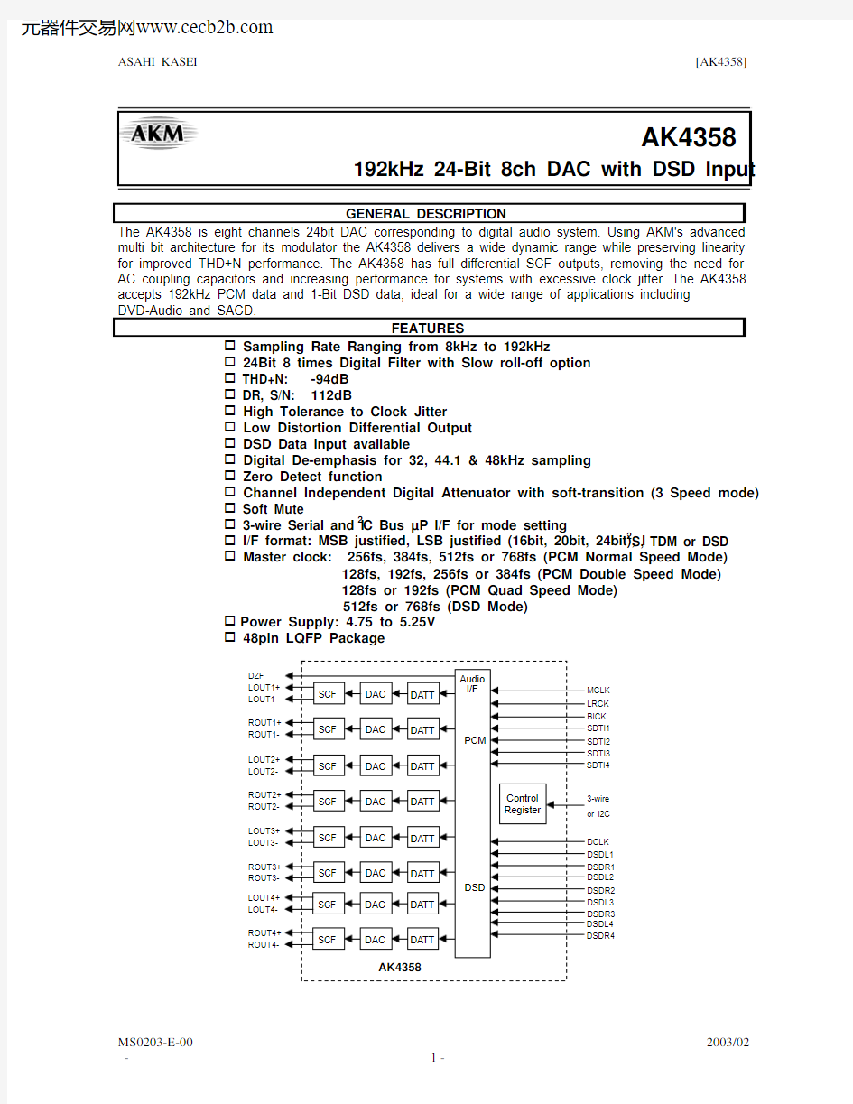
GENERAL DESCRIPTION
The AK4358 is eight channels 24bit DAC corresponding to digital audio system. Using AKM's advanced multi bit architecture for its modulator the AK4358 delivers a wide dynamic range while preserving linearity for improved THD+N performance. The AK4358 has full differential SCF outputs, removing the need for AC coupling capacitors and increasing performance for systems with excessive clock jitter. The AK4358 accepts 192kHz PCM data and 1-Bit DSD data, ideal for a wide range of applications including
DVD-Audio and SACD.
FEATURES
Sampling Rate Ranging from 8kHz to 192kHz
24Bit 8 times Digital Filter with Slow roll-off option
THD+N: -94dB
DR, S/N: 112dB
High Tolerance to Clock Jitter
Low Distortion Differential Output
DSD Data input available
Digital De-emphasis for 32, 44.1 & 48kHz sampling
Zero Detect function
Channel Independent Digital Attenuator with soft-transition (3 Speed mode)
Soft Mute
3-wire Serial and I2C Bus μP I/F for mode setting
I/F format: MSB justified, LSB justified (16bit, 20bit, 24bit), I2S, TDM or DSD
Master clock: 256fs, 384fs, 512fs or 768fs (PCM Normal Speed Mode)
128fs, 192fs, 256fs or 384fs (PCM Double Speed Mode)
128fs or 192fs (PCM Quad Speed Mode)
512fs or 768fs (DSD Mode)
Power Supply: 4.75 to 5.25V
48pin LQFP Package
DZF
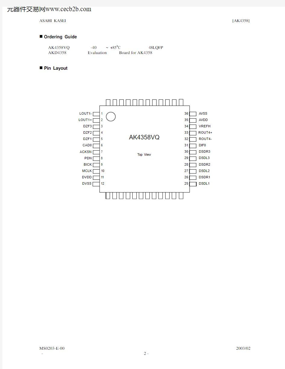
Ordering Guide
AK4358VQ -40 ~ +85°C 48LQFP AKD4358 Evaluation Board for AK4358
Pin Layout
LOUT1-
R
O
U
T
1
+ 1
LOUT1+
4
8 2
DZF3 3 DZF2 4 DZF1 5 CAD0 6 ACKSN7
PDN8
BICK9 MCLK10 DVDD
R
O
U
T
1
-
4
7
L
O
U
T
2
+
4
6
4
5
4
4
R
O
U
T
2
-
4
3
L
O
U
T
3
+
4
2
L
O
U
T
3
-
4
1
R
O
U
T
3
+
4
R
O
U
T
3
-
3
9
L
O
U
T
4
+
3
8
S
D
T
I
4
1
3
S
D
T
I
1
1
4
S
D
T
I
2
1
5
S
D
T
I
3
1
6
L
R
C
K
1
7
1
8
C
C
L
K
/
S
C
L
1
9
C
D
T
I
/
S
D
A
2
C
S
N
/
C
A
D
1
2
1
D
C
L
K
2
2
D
S
D
L
4
2
3
36
35
34
33
32
31
30
29
28
27
26
AVSS
AVDD
VREFH
ROUT4+
ROUT4-
DIF0
DSDR3
DSDL3
DSDR2
DSDL2
DSDR1 AK4358VQ
Top View
I
2
C
L
O
U
T
2
-
R
O
U
T
2
+
L
O
U
T
4
-
3
7
D
S
D
R
4
2
4
11
DVSS12 25DSDL1
Compatibility with AK4357
1. Function & Performance
AK4358 Functions AK4357
# of channels 6 8
112dB DR 106dB
48kHz/96kHz TDM Not available Available
Available I2C Not
available
DSDM control Pin/Register Register
Input channel of DZF pin Fixed Programmable
2. Pin Configuration
Pin # AK4357 AK4358
3 DZFL1 DZF3
4 DZFR1 DZF2
5 DZF23 DZF1
7 CAD1 ACKSN
12 NC DVSS
13 DVSS SDTI4
18 SMUTE I2C
19 CCLK CCLK/SCL
20 CDTI CDTI/SDA
21 CSN CSN/CAD1
22 DSDM DCLK
23 DCLK DSDL4
24 NC DSDR4
32 DIF1 ROUT4-
33 DIF2 ROUT4+
37 AVSS LOUT4-
38 AVSS LOUT4-
3. Register
Addr Bit AK4357 AK4358
00H D5 DZFM 0
01H D6 0 PW4
04H D7 ATT7 ATTE
05H D7 ATT7 ATTE
06H D7 ATT7 ATTE
07H D7 ATT7 ATTE
08H D7 ATT7 ATTE
09H D7 ATT7 ATTE
0AH D7, D6 0, 0 TDM1, TDM0
0BH Not available LOUT4 ATT Control
0CH Not available ROUT4 ATT Control
0DH Not available DZF1 control
0EH Not available DZF2 control
0FH Not available DZF3 control
PIN/FUNCTION
Name I/O Function
No. Pin
1 LOUT1- O DAC1 Lch Negative Analog Output Pin
2 LOUT1+ O DAC1 Lch Positive Analog Output Pin
3 DZF3 O Zero Input Detect 3 Pin
4 DZF2 O Zero Input Detect 2 Pin
5 DZF1 O Zero Input Detect 1 Pin
6 CAD0 I Chip Address 0 Pin
7 ACKSN I Auto Setting Mode Disable Pin (Pull-down Pin)
“L”: Auto Setting Mode, “H”: Manual Setting Mode
Pin
8 PDN I Power-Down
Mode
When at “L”, the AK4358 is in the power-down mode and is held in reset.
The AK4358 should always be reset upon power-up.
9 BICK I Audio Serial Data Clock Pin
10 MCLK I Master Clock Input Pin
An external TTL clock should be input on this pin.
11 DVDD - Digital Power Supply Pin, +4.75~+5.25V
Pin
Ground
12 DVSS - Digital
13 SDTI4 I DAC4 Audio Serial Data Input Pin
14 SDTI1 I DAC1 Audio Serial Data Input Pin
15 SDTI2 I DAC2 Audio Serial Data Input Pin
16 SDTI3 I DAC3 Audio Serial Data Input Pin
17 LRCK I L/R Clock Pin
18 I2C I Control Mode Select Pin
“L”: 3-wire Serial, “H”: I2C Bus
19 CCLK/SCL I Control Data Clock Pin
I2C = “L”: CCLK (3-wire Serial), I2C = “H”: SCL (I2C Bus)
20 CDTI/SDA I/O Control Data Input Pin
I2C = “L”: CDTI (3-wire Serial), I2C = “H”: SDA (I2C Bus)
Pin
Select
21 CSN/CAD1 I Chip
I2C = “L”: CSN (3-wire Serial), I2C = “H”: CAD1 (I2C Bus)
Pin
Clock
22 DCLK I DSD
23 DSDL4 I DAC4 DSD Lch Data Input Pin
24 DSDR4 I DAC4 DSD Rch Data Input Pin
25 DSDL1 I DAC1 DSD Lch Data Input Pin
26 DSDR1 I DAC1 DSD Rch Data Input Pin
27 DSDL2 I DAC2DSD Lch Data Input Pin
28 DSDR2 I DAC2 DSD Rch Data Input Pin
29 DSDL3 I DAC3 DSD Lch Data Input Pin
30 DSDR3 I DAC3 DSD Rch Data Input Pin
31 DIF0 I Audio Data Interface Format 0 Pin
32 ROUT4- O DAC4 Rch Negative Analog Output Pin
33 ROUT4+ O DAC4 Rch Positive Analog Output Pin
34 VREFH I Positive Voltage Reference Input Pin
35 AVDD - Analog Power Supply Pin, +4.75~+5.25V
36 AVSS - Analog Ground Pin
37 LOUT4- O DAC4 Lch Negative Analog Output Pin
38 LOUT4+ O DAC4 Lch Positive Analog Output Pin
39 ROUT3- O DAC3 Rch Negative Analog Output Pin
40 ROUT3+ O DAC3 Rch Positive Analog Output Pin
41 LOUT3- O DAC3 Lch Negative Analog Output Pin
42 LOUT3+ O DAC3 Lch Positive Analog Output Pin
43 ROUT2- O DAC2 Rch Negative Analog Output Pin
44 ROUT2+ O DAC2 Rch Positive Analog Output Pin
45 LOUT2- O DAC2 Lch Negative Analog Output Pin
46 LOUT2+ O DAC2 Lch Positive Analog Output Pin
47 ROUT1- O DAC1 Rch Negative Analog Output Pin
48 ROUT1+ O DAC1 Rch Positive Analog Output Pin
Note: All input pins except pull-down pin should not be left floating.
ABSOLUTE MAXIMUM RATINGS
(AVSS, DVSS=0V; Note 1)
Parameter Symbol
Min
Max
Units
Power Supplies Analog
Digital
|AVSS-DVSS| (Note 2)AVDD
DVDD
?GND
-0.3
-0.3
-
6.0
6.0
0.3
V
V
V
Input Current (any pins except for supplies) IIN - ±10 mA
Analog Input Voltage VINA -0.3 AVDD+0.3 V
Digital Input Voltage VIND -0.3 DVDD+0.3 V
Ambient Operating Temperature Ta -40 85 °C
Storage Temperature Tstg -65 150 °C
Note 1. All voltages with respect to ground.
Note 2. AVSS and DVSS must be connected to the same analog ground plane.
WARNING: Operation at or beyond these limits may result in permanent damage to the device.
Normal operation is not guaranteed at these extremes.
RECOMMENDED OPERATING CONDITIONS
(AVSS, DVSS=0V; Note 1)
Parameter Symbol
Min
Typ
Max
Units
Power Supplies (Note 3) Analog
Digital
AVDD
DVDD
4.75
4.75
5.0
5.0
5.25
5.25
V
V
Voltage Reference VREF AVDD-0.5- AVDD V Note 3. The power up sequence between AVDD and DVDD is not critical.
*AKM assumes no responsibility for the usage beyond the conditions in this datasheet.
ANALOG CHARACTERISTICS
(Ta=25°C; AVDD, DVDD=5V; VREFH=AVDD; fs=44.1kHz; BICK=64fs; Signal Frequency=1kHz; 24bit Input Data;
Measurement frequency=20Hz ~ 20kHz; R L ≥2k?; unless otherwise specified)
Parameter Min
Typ
Max
Units Resolution
24
Bits Dynamic Characteristics (Note 4)
fs=44.1kHz BW=20kHz 0dBFS
-60dBFS
-94
-48
-86
-
dB
dB
fs=96kHz BW=40kHz 0dBFS
-60dBFS
-92
-45
-84
-
dB
dB
THD+N
fs=192kHz BW=40kHz 0dBFS
-60dBFS
-92
-45
-
-
dB
dB
Dynamic Range (-60dBFS with A-weighted) (Note 5) 102 112 dB S/N (A-weighted) (Note 6) 102 112 dB Interchannel Isolation (1kHz) 90 100 dB Interchannel Gain Mismatch 0.2 0.5 dB DC Accuracy
Gain Drift 100 - ppm/°C Output Voltage (Note 7) ±2.35 ±2.5 ±2.65 Vpp Load Resistance (Note 8) 2 k?Power Supplies
Power Supply Current (AVDD+DVDD)
Normal Operation (PDN = “H”, fs≤96kHz) (Note 9) Normal Operation (PDN = “H”, fs=192kHz) (Note 10) Power-Down Mode (PDN = “L”) (Note 11)56
62
10
70
85
100
mA
mA
μA
Note 4. Measured by Audio Precision System Two. Refer to the evaluation board manual.
Note 5. 100dB at 16bit data.
Note 6. S/N does not depend on input bit length.
Note 7. Full scale voltage (0dB). Output voltage scales with the voltage of VREFH pin. AOUT (typ. @0dB) = (AOUT+)-(AOUT-) = ±2.5Vpp×VREFH/5.0
Note 8. For AC-load. 4k? for DC-load
Note 9 AVDD=40mA(Typ), DVDD=12mA(Typ)@44.1kHz&5V, 16mA(Typ)@96kHz&5V
Note 10 AVDD=40mA(Typ), DVDD=22mA(Typ)@192kHz&5V
Note 11. All digital inputs including clock pins (MCLK, BICK and LRCK) are held DVDD or DVSS.
SHARP ROLL-OFF FILTER CHARACTERISTICS
(Ta = 25°C; AVDD, DVDD = 4.75 ~ 5.25V; fs = 44.1kHz; DEM = OFF; SLOW = “0”; PCM Mode)
Parameter Symbol
Min
Typ
Max
Units Digital filter
Passband ±0.05dB (Note 12) -6.0dB PB 0
- 22.05
20.0
-
kHz
kHz
Stopband (Note 12) SB 24.1 kHz Passband Ripple PR ± 0.02 dB Stopband Attenuation SA 54 dB Group Delay (Note 13) GD - 19.1 - 1/fs Digital Filter + SCF
Frequency Response 20.0kHz
40.0kHz
80.0kHz Fs=44.1kHz
Fs=96kHz
Fs=192kHz
FR
FR
FR
-
-
-
± 0.2
± 0.3
+0/-0.6
-
-
-
dB
dB
dB
Note 12. The passband and stopband frequencies scale with fs(system sampling rate). For example, PB=0.4535×fs (@±0.05dB), SB=0.546×fs.
Note 13. The calculating delay time which occurred by digital filtering. This time is from setting the 16/24bit data of both channels to input register to the output of analog signal.
SLOW ROLL-OFF FILTER CHARACTERISTICS
(Ta = 25°C; AVDD, DVDD = 4.75~5.25V; fs = 44.1kHz; DEM = OFF; SLOW = “1”; PCM Mode)
Parameter Symbol Min Typ Max Units Digital Filter
Passband ±0.04dB (Note 14) -3.0dB PB 0
- 18.2
8.1
-
kHz
kHz
Stopband (Note 14) SB 39.2 kHz Passband Ripple PR ± 0.005 dB Stopband Attenuation SA 72 dB Group Delay (Note 13) GD - 19.1 - 1/fs Digital Filter + SCF
Frequency Response 20.0kHz
40.0kHz
80.0kHz fs=44.kHz
fs=96kHz
fs=192kHz
FR
FR
FR
-
-
-
+0/-5
+0/-4
+0/-5
-
-
-
dB
dB
dB
Note 14. The passband and stopband frequencies scale with fs. For example, PB = 0.185×fs (@±0.04dB), SB = 0.888×fs.
DC CHARACTERISTICS
(Ta = 25°C; AVDD, DVDD = 4.75 ~ 5.25V)
Parameter Symbol
Min
Typ
Max
Units
High-Level Input Voltage Low-Level Input Voltage VIH
VIL
2.2
-
-
-
-
0.8
V
V
High-Level Output Voltage (Iout = -80μA) Low-Level Output Voltage (Iout = 80μA) VOH
VOL
DVDD-0.4
-
- -
0.4
V
V
Input Leakage Current (Note 15) Iin - - ± 10 μA Note 15. ACKSN pin has internal pull-down devices, nominally 100k?.
SWITCHING CHARACTERISTICS
(Ta = 25°C; AVDD, DVDD = 4.75 ~ 5.25V; C L = 20pF)
Parameter Symbol
Min
Typ
Max
Units
Master Clock Frequency Duty Cycle fCLK
dCLK
2.048
40
11.2896 36.864
60
MHz
%
LRCK Frequency
Normal Mode (TDM0= “L”, TDM1= “L”)
Normal Speed Mode Double Speed Mode Quad Speed Mode Duty Cycle
fsn
fsd
fsq
Duty
8
60
120
45
48
96
192
55
kHz
kHz
kHz
%
TDM256 mode (TDM0= “H”, TDM1= “L”)
Normal Speed Mode High time
Low time
fsn
tLRH
tLRL
32
1/256fs
1/256fs
48 kHz
ns
ns
TDM128 mode (TDM0= “H”, TDM1= “H”)
Normal Speed Mode Double Speed Mode High time
Low time
fsn
fsd
tLRH
tLRL
32
60
1/128fs
1/128fs
48
96
kHz
kHz
ns
ns
PCM Audio Interface Timing
BICK Period
BICK Pulse Width Low
Pulse Width High
BICK “↑” to LRCK Edge (Note 16) LRCK Edge to BICK “↑” (Note 16) SDTI Hold Time
SDTI Setup Time
tBCK
tBCKL
tBCKH
tBLR
tLRB
tSDH
tSDS
81
30
30
20
20
10
10
ns
ns
ns
ns
ns
ns
ns
DSD Audio Interface Timing
DCLK Period
DCLK Pulse Width Low
Pulse Width High
DCLK Edge to DSDL/R (Note 17)
tDCK
tDCKL
tDCKH
tDDD
1/64fs
160
160
-20 20
ns
ns
ns
ns
Control Interface Timing (3-wire Serial mode):
CCLK Period
CCLK Pulse Width Low Pulse Width High CDTI Setup Time
CDTI Hold Time
CSN High Time
CSN “↓” to CCLK “↑” CCLK “↑” to CSN “↑”
tCCK
tCCKL
tCCKH
tCDS
tCDH
tCSW
tCSS
tCSH
200
80
80
40
40
150
50
50
ns
ns
ns
ns
ns
ns
ns
ns
Control Interface Timing (I2C Bus mode):
SCL Clock Frequency
Bus Free Time Between Transmissions
Start Condition Hold Time (prior to first clock pulse) Clock Low Time
Clock High Time
Setup Time for Repeated Start Condition
SDA Hold Time from SCL Falling (Note 18) SDA Setup Time from SCL Rising
Rise Time of Both SDA and SCL Lines
Fall Time of Both SDA and SCL Lines
Setup Time for Stop Condition
Pulse Width of Spike Noise Suppressed by Input Filter
fSCL
tBUF
tHD:STA
tLOW
tHIGH
tSU:STA
tHD:DAT
tSU:DAT
tR
tF
tSU:STO
tSP
-
4.7
4.0
4.7
4.0
4.7
0.25
-
-
4.0
100
-
-
-
-
-
-
-
1.0
0.3
-
50
kHz
μs
μs
μs
μs
μs
μs
μs
μs
μs
μs
ns
Units
Parameter Symbol
Max
Typ
Min
Reset Timing
PDN Pulse Width (Note 19) tPD 150 ns
Note 16. BICK rising edge must not occur at the same time as LRCK edge.
Note 17. DSD data transmitting device must meet this time.
Note 18. Data must be held for sufficient time to bridge the 300 ns transition time of SCL.
Note 19. The AK4358 can be reset by bringing PDN= “L”.
Note 20. I2C is a registered trademark of Philips Semiconductors.
Purchase of Asahi Kasei Microsystems Co., Ltd I2C components conveys a license under the Philips
I2C patent to use the components in the I2C system, provided the system conform to the I2C
specifications defined by Philips.
Timing Diagram
VIH
MCLK
VIL
VIH LRCK
VIL
VIH BICK
VIL
Clock Timing
LRCK
VIH BICK
VIL
VIH SDTI
VIL VIH VIL
Audio Serial Interface Timing (PCM Mode)
VIH DCLK
VIL
VIH DSDL DSDR
VIL
Audio Serial Interface Timing (DSD Normal Mode, DCKB = “0”)
VIH DCLK
VIL
VIH DSDL DSDR
VIL
Audio Serial Interface Timing (DSD Phase Modulation Mode, DCKB = “0”)
CSN
VIH CCLK
VIL
VIH CDTI VIL
VIH
VIL
WRITE Command Input Timing
CSN
VIH CCLK
VIL
VIH CDTI VIL
VIH
VIL
D3D2D1D0
WRITE Data Input Timing
VIH
VIL
VIH
VIL
I 2C Bus mode Timing
VIL
PDN
Power-down Timing
OPERATION OVERVIEW
D/A Conversion Mode
The AK4358 can perform D/A conversion for both PCM data and DSD data. When DSD mode, DSD data can be input
from DCLK, DSDL1-4 and DSDR1-4 pins. When PCM mode, PCM data can be input from BICK, SDTI1-4 and LRCK
pins. PCM/DSD mode changes by D/P bit. When PCM/DSD mode changes by D/P bit, the AK4358 should be reset by
RSTN bit, PW bit (PW1=PW2=PW3=PW4= “0”) or PDN pin. It takes about 2/fs to 3/fs to change the mode.
D/P bit DAC Output
0 PCM
1 DSD
Table 1. DSD/PCM Mode Control
System Clock
1) PCM Mode
The external clocks, which are required to operate the AK4358, are MCLK, LRCK and BICK. The master clock (MCLK)
should be synchronized with LRCK but the phase is not critical. The MCLK is used to operate the digital interpolation
filter and the delta-sigma modulator. There are two methods to set MCLK frequency. In Manual Setting Mode (ACKS = “0”: Register 00H), the sampling speed is set by DFS0/1(Table 2). The frequency of MCLK at each sampling speed is set automatically. (Table 3~Table 5). In Auto Setting Mode (ACKS = “1”: Default), as MCLK frequency is detected automatically (Table 6), and the internal master clock becomes the appropriate frequency (Table 7), it is not necessary to
set DFS0/1. When ACKSN = “H”, regardless of ACKS bit setting the AK4358 operates by Manual Setting Mode. When ACKSN = “L”, ACKS bit setting is valid.
All external clocks (MCLK, BICK and LRCK) should always be present whenever the AK4358 is in the normal operation
mode (PDN= ”H”). If these clocks are not provided, the AK4358 may draw excess current and may fall into unpredictable operation. This is because the device utilizes dynamic refreshed logic internally. The AK4358 should be reset by PDN =
“L” after threse clocks are provided. If the external clocks are not present, the AK4358 should be in the power-down
mode (PDN= ”L”). After exiting reset(PDN = “↑”) at power-up etc., the AK4358 is in the power-down mode until MCLK
is input. DSD interface signals (DCLK, DSDL1-4, DSDR1-4) are fixed to “H” or “L”.
(fs)
DFS1 DFS0 Sampling
Rate
0 0 Normal Speed Mode 8kHz~48kHz Default
0 1 Double Speed Mode 60kHz~96kHz
Mode 120kHz~192kHz
Speed
1 0
Quad
Table 2. Sampling Speed (Manual Setting Mode)
LRCK MCLK BICK
fs 256fs 384fs 512fs 768fs 64fs
32.0kHz 8.1920MHz 12.2880MHz16.3840MHz24.5760MHz 2.0480MHz
44.1kHz 11.2896MHz 16.9344MHz22.5792MHz33.8688MHz 2.8224MHz
48.0kHz 12.2880MHz 18.4320MHz24.5760MHz36.8640MHz 3.0720MHz
Table 3. System Clock Example (Normal Speed Mode @Manual Setting Mode)
LRCK MCLK BICK
fs 128fs 192fs 256fs 384fs 64fs
88.2kHz 11.2896MHz 16.9344MHz22.5792MHz33.8688MHz 5.6448MHz
96.0kHz 12.2880MHz 18.4320MHz24.5760MHz36.8640MHz 6.1440MHz
Table 4. System Clock Example (Double Speed Mode @Manual Setting Mode)
LRCK MCLK BICK
fs 128fs 192fs 64fs
176.4kHz 22.5792MHz33.8688MHz11.2896MHz
192.0kHz 24.5760MHz36.8640MHz12.2880MHz
Table 5. System Clock Example (Quad Speed Mode @Manual Setting Mode)
Speed
MCLK Sampling
512fs 768fs Normal
256fs 384fs Double
128fs 192fs Quad
Table 6. Sampling Speed (Auto Setting Mode)
(MHz)
LRCK MCLK
Sampling Speed fs 128fs 192fs 256fs 384fs 512fs 768fs
24.5760
16.3840
- - - -
32.0kHz
Normal
33.8688
22.5792
- - - -
44.1kHz
24.5760
36.8640
48.0kHz
- - - -
33.8688 - -
88.2kHz - - 22.5792
Double
96.0kHz - - 24.5760
36.8640 - -
- - - -
33.8688
22.5792
176.4kHz
Quad
24.5760
- - - - 192.0kHz
36.8640
Table 7. System Clock Example (Auto Setting Mode)
ACKSN pin ACKS bit Clock Mode
Mode
Setting
0 0
Manual
0 1 Auto Setting Mode (Default)
Mode
Setting
1 0
Manual
Mode
Setting
Manual
1 1
Table 8. Relationship between ACKSN pin and ACKS bit
2) DSD Mode
The external clocks, which are required to operate the AK4358, are MCLK and DCLK. The master clock (MCLK) should
be synchronized with DSD clock (DCLK) but the phase is not critical. The frequency of MCLK is set by DCKS bit.
All external clocks (MCLK, DCLK) should always be present whenever the AK4358 is in the normal operation mode
(PDN= ”H”). If these clocks are not provided, the AK4358 may draw excess current because the device utilizes dynamic refreshed logic internally. The AK4358 should be reset by PDN= ”L” after threse clocks are provided. If the external
clocks are not present, the AK4358 should be in the power-down mode (PDN= ”L”). After exiting reset(PDN = “↑”) at
power-up etc., the AK4358 is in the power-down mode until MCLK is input. PCM interface signals (BICK, LRCK,
SDTI1-4) are fixed to “H” or “L”.
DCKS 0 1 MCLK 512fs 768fs DCLK 64fs 64fs Table 9. System Clock (fs=44.1kHz)
Audio Serial Interface Format
1) PCM Mode
When PCM mode, data is shifted in via the SDTI1-4 pins using BICK and LRCK inputs. The DIF0-2 as shown in Table 10 can select five serial data modes. Initial value of DIF0-2 bits is “010” and DIF0 bit is ORed with DIF0 pin. In all modes the serial data is MSB-first, 2’s compliment format and is latched on the rising edge of BICK. Mode 2 can be used for 16/20 MSB justified formats by zeroing the unused LSBs.
When TDM0 = “1”, the audio interface becomes TDM mode. In TDM256 mode (TDM1 = “0”, Table 11), the serial data of all DAC (eight channels) is input to the SDTI1 pin. The input data to SDTI2-4 pins is ignored. BICK should be fixed to 256fs. “H” time and “L” time of LRCK should be 1/256fs at least. The serial data is MSB-first, 2’s compliment format. The input data to SDTI1 pin is latched on the rising edge of BICK. In TDM128 mode (TDM1 = “1”, Table 12), the serial data of DAC (four channels; L1, R1, L2, R2) is input to the SDTI1 pin. Other four data (L3, R3, L4, R4) is input to the SDTI2. The input data to SDTI3-4 pins is ignored. BICK should be fixed to 128fs.
Mode TDM1 TDM0 DIF2 DIF1DIF0SDTI Format LRCK BICK Figure 0 0 0 0 0 0 16bit LSB Justified H/L ≥32fs Figure 1 1 0 0 0 0 1 20bit LSB Justified H/L ≥40fs Figure 22 0 0 0 1 0 24bit MSB Justified H/L ≥48fs Figure 3Default 3 0 0 0 1 1 24bit I 2S Compatible L/H ≥48fs Figure 4 4 0 0 1 0 0 24bit LSB Justified H/L ≥48fs Figure 2
Table 10. Audio Data Formats (Normal mode)
SDTI BICK
LRCK
SDTI BICK (32fs)(64fs)Mode 0
Mode 0
Figure 1. Mode 0 Timing
SDTI LRCK BICK (64fs)
Mode 1SDTI Mode 4
Figure 2. Mode 1,4 Timing
LRCK
BICK (64fs)SDTI
Figure 3. Mode 2 Timing
LRCK
BICK (64fs)SDTI
Figure 4. Mode 3 Timing
0 1 0 0 0 N/A 0 1 0 0 1 N/A 5 0 1 0 1 0 24bit MSB Justified ↑
256fs Figure 5 6 0 1 0 1 1 24bit I 2
S
Compatible
↓
256fs Figure 6 7 0 1 1 0 0 24bit LSB Justified ↑
256fs Figure 7Table 11. Audio Data Formats (TDM256 mode)
LRCK BICK(256fs) SDTI1(i)
Figure 5. Mode 5 Timing
LRCK BICK(256fs) SDTI1(i)
Figure 6. Mode 6 Timing
LRCK BICK(256fs) SDTI1(i)
Figure 7. Mode 7 Timing
1 1 0 0 0 N/A 1 1 0 0 1 N/A
8 1 1 0 1 0 24bit MSB Justified
↑ 128fs Figure 8 9 1 1 0 1 1
24bit I 2
S
Compatible
↓
128fs Figure 9 10 1 1 1 0 0 24bit LSB Justified ↑
128fs
Figure
10
Table 12. Audio Data Formats (TDM128 mode)
LRCK BICK(128fs)
SDTI1(i)
SDTI2(i)
Figure 8. Mode 8 Timing
LRCK BICK(128fs)
SDTI1(i)
SDTI2(i)
Figure 9. Mode 9 Timing
LRCK BICK(128fs)
SDTI1(i)
SDTI2(i)
Figure 10. Mode 10 Timing
2) DSD Mode
In case of DSD mode, DIF0-2 is ignored. The frequency of DCLK is fixed to 64fs. DCKB bit can invert the polarity of DCLK.
DCLK (64fs) DCKB=1
DCLK (64fs) DCKB=0DSDL,DSDR Normal DSDL,DSDR
Phase Modulation
D1
D0D1D2D0
D2
D3
D1D2D3
Figure 11. DSD Mode Timing
D/A conversion mode switching timing
RSTN bit
D/A Data
D/A Mode
Figure 12. D/A Mode Switching Timing (PCM to DSD)
RSTN bit
D/A Data
D/A Mode
Figure 13. D/A Mode Switching Mode Timing (DSD to PCM)
Caution: In DSD mode, the signal level is ranging from 25% to 75%. Peak levels of DSD signal above this duty are not
recommended by SACD format book (Scarlet Book).
De-emphasis Filter
A digital de-emphasis filter is available for 32, 44.1 or 48kHz sampling rates (tc = 50/15μs) and is enabled or disabled with DEM0 and DEM1. In case of double speed and quad speed mode, the digital de-emphasis filter is always off. When DSD mode, DEM0-1 is invalid.
DEM1DEM0Mode
44.1kHz
0 0
Default
0 1 OFF
1 0 48kHz
1 1 32kHz
Table 13. De-emphasis Filter Control (Normal Speed Mode)
Output Volume
The AK4358 includes channel independent digital output volumes (ATT) with 128 levels at 0.5dB steps including SMUTE. These volumes are in front of the DAC and can attenuate the input data from 0dB to –63dB and mute. Transition time is set by AST1-0 bits(Table 15) When changing levels, transitions are executed via soft changes; thus no switching noise occurs during these transitions. When ATTE bit is set to “0”, the DAC input data goes to “0” immediately. It takes a time of group delay to mute the analog output. ATTE bit should be “1” to enable the volume setting.
ATTE ATT6-0 Attenuation
Level
Default
7FH 0dB
7EH -0.5dB
7DH -1.0dB
1
: :
02H -62.5dB
01H -63.0dB
00H SMUTE (-∞)
0 Don’t care OFF ( “0” )
Table 14. Attenuation Level of Output Volume
Mode ATS1 ATS0 ATT
speed
Default
0 0 0 1792/fs
1 0 1 896/fs
2 1 0 256/fs
3 1 1 N/A
Table 15. Transition time of output volume
In case of Mode 0, it takes 1792/fs to transit from 7FH(0dB) to 00H(SMUTE). In case Mode1, it takes 896/fs to transit from 7FH(0dB) to 00H(SMUTE). In case Mode2 and 3,it takes 256/fs to transit from 7FH(0dB) to 00H (SMUTE). If PDN pin goes to “L”, ATT6-0 registers are initialized to 7FH.ATT6-0 registers go to 7FH when RSTN bit is set to “0”. When RSTN bit returns to “1”, ATT6-0 registers go to the set value. Digital output volume function is independent of soft mute function.
The setting value of the register is held when switching between PCM mode and DSD mode.