MMBTA92L, SMMBTA92L, MMBTA93L
High Voltage Transistors PNP Silicon
Features
?AEC?Q101 Qualified and PPAP Capable
?S Prefix for Automotive and Other Applications Requiring Unique Site and Control Change Requirements
?These Devices are Pb?Free, Halogen Free/BFR Free and are RoHS Compliant
MAXIMUM RATINGS
Rating Symbol9293Unit Collector?Emitter Voltage V CEO?300?200Vdc Collector?Base Voltage V CBO?300?200Vdc Emitter?Base Voltage V EBO?5.0?5.0Vdc Collector Current — Continuous I C?500mAdc DEVICE MARKING
MMBTA92L, SMMBTA92L = 2D; MMBTA93LT1 = 2E
THERMAL CHARACTERISTICS
Characteristic Symbol Max Unit Total Device Dissipation FR
?5 Board (Note 1) T A = 25°C
Derate above 25°C P D225
1.8
mW
mW/°C
Thermal Resistance, Junction to Ambient R q JA556°C/W
Total Device Dissipation (Note 2) Alumina Substrate,(2) T A = 25°C Derate above 25°C P D300
2.4
mW
mW/°C
Thermal Resistance, Junction to Ambient R q JA417°C/W Junction and Storage Temperature T J, T
stg?55 to
+150°C
Stresses exceeding Maximum Ratings may damage the device. Maximum Ratings are stress ratings only. Functional operation above the Recommended Operating Conditions is not implied. Extended exposure to stresses above the Recommended Operating Conditions may affect device reliability.
1.FR?5 = 1.0 x 0.75 x 0.062 in.
2.Alumina = 0.4 x 0.3 x 0.024 in. 99.5% alumina.
https://www.doczj.com/doc/9f5656046.html,
Device Package Shipping?
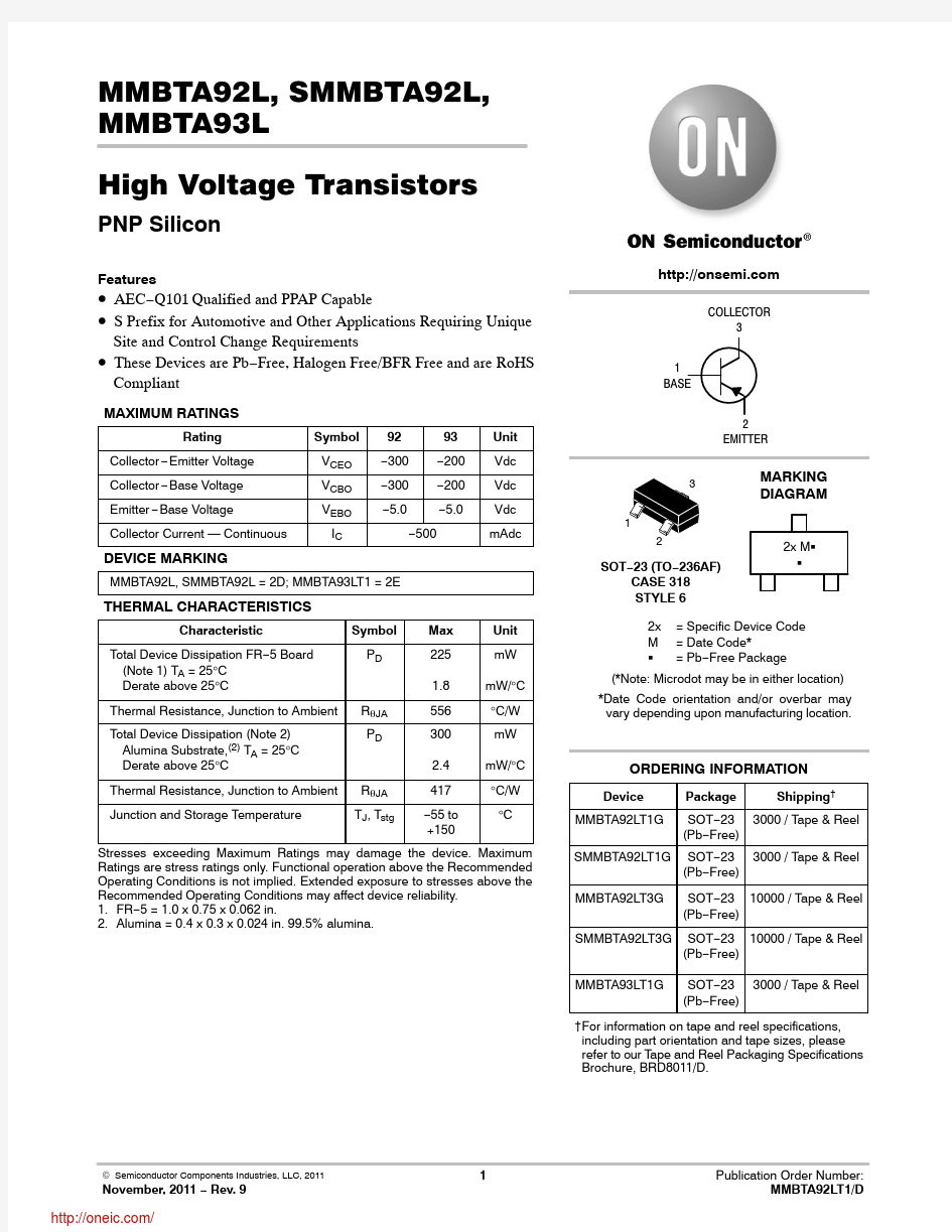
ORDERING INFORMATION
MMBTA92LT1G SOT?23
(Pb?Free)
SOT?23 (TO?236AF)
CASE 318
STYLE 6
3000 / Tape & Reel
MARKING
DIAGRAM
2x M G
G
2x= Specific Device Code
M= Date Code*
G= Pb?Free Package
COLLECTOR
1
EMITTER
MMBTA92LT3G SOT?23
(Pb?Free)
10000 / Tape & Reel
?For information on tape and reel specifications, including part orientation and tape sizes, please refer to our T ape and Reel Packaging Specifications Brochure, BRD8011/D.
(*Note: Microdot may be in either location)
*Date Code orientation and/or overbar may
vary depending upon manufacturing location.
MMBTA93LT1G SOT?23
(Pb?Free)
3000 / Tape & Reel SMMBTA92LT1G SOT?23
(Pb?Free)
3000 / Tape & Reel
SMMBTA92LT3G SOT?23
(Pb?Free)
10000 / Tape & Reel
ELECTRICAL CHARACTERISTICS (T A = 25°C unless otherwise noted)
Characteristic
Symbol
Min
Max
Unit
OFF CHARACTERISTICS
Collector ?Emitter Breakdown Voltage (Note 3)(I C = ?1.0 mAdc, I B = 0)
MMBTA92, SMMBTA92
MMBTA93V (BR)CEO
?300?200??
Vdc
Collector ?Base Breakdown Voltage (I C = ?100 m Adc, I E = 0)MMBTA92, SMMBTA92
MMBTA93
V (BR)CBO
?300?200??Vdc
Emitter ?Base Breakdown Voltage (I E = ?100 m Adc, I C = 0)V (BR)EBO ?5.0
?
Vdc Collector Cutoff Current (V CB = ?200 Vdc, I E = 0)MMBTA92, SMMBTA92
(V CB = ?160 Vdc, I E = 0)MMBTA93I CBO
???0.25?0.25m Adc
Emitter Cutoff Current (V EB = ?3.0 Vdc, I C = 0)
I EBO
?
?0.1
m Adc
ON CHARACTERISTICS (Note 3)
DC Current Gain
(I C = ?1.0 mAdc, V CE = ?10 Vdc)Both Types (I C = ?10 mAdc, V CE = ?10 Vdc)Both Types
(I C = ?30 mAdc, V CE = ?10 Vdc)MMBTA92, SMMBTA92
MMBTA93h FE
25402525????
?
Collector ?Emitter Saturation Voltage (I C = ?20 mAdc, I B = ?2.0 mAdc)MMBTA92, SMMBTA92
MMBTA93
V CE(sat)???0.5?0.5Vdc
Base ?Emitter Saturation Voltage (I C = ?20 mAdc, I B = ?2.0 mAdc)
V BE(sat)
?
?0.9
Vdc
SMALL ?SIGNAL CHARACTERISTICS
Current ?Gain — Bandwidth Product
(I C = ?10 mAdc, V CE = ?20 Vdc, f = 100 MHz)f T 50
?
MHz Collector ?Base Capacitance
(V CB = ?20 Vdc, I E = 0, f = 1.0 MHz)
MMBTA92, SMMBTA92
MMBTA93
C cb
??
6.08.0
pF
3.Pulse Test: Pulse Width v 300 m s, Duty Cycle v 2.0%.
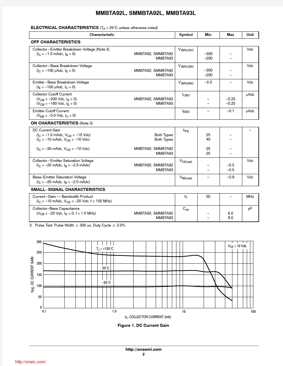
Figure 1. DC Current Gain
I C , COLLECTOR CURRENT (mA)
3000.1 1.0
10250200
1500
h F E , D C C U R R E N T G A I N
100
50100
Figure 2. Capacitance I C, COLLECTOR CURRENT (mA)
f
?
,
C
U
R
R
E
N
T
-
G
A
I
N
—
B
A
N
D
W
I
D
T
H
(
M
H
z
)
T
1
Figure 3. Current?Gain ? Bandwidth
C
,
C
A
P
A
C
I
T
A
N
C
E
(
p
F
)
V R, REVERSE VOLTAGE (VOLTS)
100
I C, COLLECTOR CURRENT (mA)
V
,
V
O
L
T
A
G
E
(
V
O
L
T
S
)
1.4
0.0
1.2
1.0
0.8
0.6
0.4
0.2
100
10
0.1 1.0
3579
Figure 4. “ON” Voltages
Figure 5. Safe Operating Area
V CE, COLLECTOR?EMITTER VOLTAGE (V)
I
C
,
C
O
L
L
E
C
T
O
R
C
U
R
R
E
N
T
(
A
)
PACKAGE DIMENSIONS
STYLE 6:
PIN 1.BASE
2.EMITTER
3.COLLECTOR
SOT ?23 (TO ?236)CASE 318?08ISSUE AP
SOLDERING FOOTPRINT
NOTES:
1.DIMENSIONING AND TOLERANCING PER ANSI Y14.5M, 198
2.2.CONTROLLING DIMENSION: INCH.
3.MAXIMUM LEAD THICKNESS INCLUDES LEAD FINISH
THICKNESS. MINIMUM LEAD THICKNESS IS THE MINIMUM THICKNESS OF BASE MATERIAL.
4.DIMENSIONS D AND E DO NOT INCLUDE MOLD FLASH,PROTRUSIONS, OR GATE BURRS.
VIEW C
DIM A MIN NOM MAX MIN
MILLIMETERS
0.89 1.00 1.110.035INCHES A10.010.060.100.001b 0.370.440.500.015c 0.090.130.180.003D 2.80 2.90 3.040.110E 1.20 1.30 1.400.047e 1.78 1.90 2.040.070L 0.100.200.300.0040.0400.0440.0020.0040.0180.0200.0050.0070.1140.1200.0510.0550.0750.0810.0080.012NOM MAX L1 2.10 2.40 2.640.0830.0940.104H E 0.350.540.690.0140.0210.0290???100???
10q
°
°
°
°
ON Semiconductor and are registered trademarks of Semiconductor Components Industries, LLC (SCILLC). SCILLC reserves the right to make changes without further notice
to any products herein. SCILLC makes no warranty, representation or guarantee regarding the suitability of its products for any particular purpose, nor does SCILLC assume any liability arising out of the application or use of any product or circuit, and specifically disclaims any and all liability, including without limitation special, consequential or incidental damages.“Typical” parameters which may be provided in SCILLC data sheets and/or specifications can and do vary in different applications and actual performance may vary over time. All operating parameters, including “Typicals” must be validated for each customer application by customer’s technical experts. SCILLC does not convey any license under its patent rights nor the rights of others. SCILLC products are not designed, intended, or authorized for use as components in systems intended for surgical implant into the body, or other applications intended to support or sustain life, or for any other application in which the failure of the SCILLC product could create a situation where personal injury or death may occur. Should Buyer purchase or use SCILLC products for any such unintended or unauthorized application, Buyer shall indemnify and hold SCILLC and its officers, employees, subsidiaries, affiliates,and distributors harmless against all claims, costs, damages, and expenses, and reasonable attorney fees arising out of, directly or indirectly, any claim of personal injury or death associated with such unintended or unauthorized use, even if such claim alleges that SCILLC was negligent regarding the design or manufacture of the part. SCILLC is an Equal Opportunity/Affirmative Action Employer. This literature is subject to all applicable copyright laws and is not for resale in any manner.
PUBLICATION ORDERING INFORMATION
分销商库存信息:
ONSEMI
MMBTA92LT1G MMBTA92LT3G SMMBTA92LT1G SMMBTA92LT3G MMBTA93LT1G