HD74AC244/HD74ACT244
Octal Buffer/Line Driver with 3-State Output
REJ03D0262–0200Z
(Previous ADE-205-383 (Z))
Rev.2.00
Jul.16.2004 Description
The HD74AC244/HD74ACT244 is an octal buffer and line driver designed to be employed as a memory address driver, clock driver and bus-oriented transmitter/receive which provides improved PC board density.
Features
?3-State Outputs Drive Bus Lines or Buffer Memory Address Registers
?Outputs Source/Sink 24 mA
?HD74ACT244 has TTL-Compatible Inputs
?Ordering Information: Ex. HD74AC244
Part Name Package Type Package Code Package Abbreviation Taping Abbreviation (Quantity) HD74AC244P DIP-20 pin DP-20N, -20NEV P—
HD74AC244FPEL SOP-20 pin (JEITA)FP-20DAV FP EL (2,000 pcs/reel)
HD74AC244RPEL SOP-20 pin (JEDEC)FP-20DBV RP EL (1,000 pcs/reel)
HD74AC244TELL TSSOP-20 pin TTP-20DAV T ELL (2,000 pcs/reel)
Notes: 1.Please consult the sales office for the above package availability.
2.The packages with lead-free pins are distinguished from the conventional products by adding V at the end of
the package code.
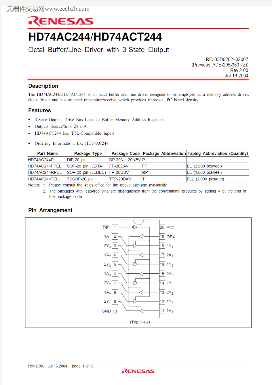
Pin Arrangement
Truth Tables
Inputs Outputs (Pins 12, 14, 16, 18)
OE 1
A
Y
L L L L H H H
X
Z
Inputs Outputs (Pins 3, 5, 7, 9)
OE 2
A
Y
L L L L H H H X
Z
H :High Voltage Level L :Low Voltage Level X :Immaterial
Z
:
High Impedance
Absolute Maximum Ratings
Item
Symbol Ratings
Unit Condition Supply voltage
V CC –0.5 to 7V –20
mA V I = –0.5V DC input diode current I IK 20
mA V I = Vcc+0.5V DC input voltage V I –0.5 to Vcc+0.5V –50mA V O = –0.5V DC output diode current I OK 50
mA V O = Vcc+0.5V
DC output voltage
V O –0.5 to Vcc+0.5V DC output source or sink current I O
±50mA DC V CC or ground current per output pin I CC , I GND ±50
mA Storage temperature
Tstg
–65 to +150
°C
Recommended Operating Conditions: HD74AC244
Item
Symbol Ratings
Unit
Condition
Supply voltage
V CC 2 to 6V Input and Output voltage V I , V O 0 to V CC V Operating temperature Ta –40 to +85°C V CC = 3.0V V CC = 4.5 V Input rise and fall time (except Schmitt inputs)V IN 30% to 70% V CC
tr, tf
8
ns/V
V CC = 5.5 V
+85°C bol (V)min.typ.max.min.max.3.0 2.1 1.5— 2.1—4.5 3.15 2.25— 3.15—V IH
5.5
3.85 2.75— 3.85—V OUT = 0.1 V or V CC –0.1 V
3.0— 1.500.9—0.9
4.5— 2.25 1.35— 1.35Input Voltage V IL
5.5— 2.75 1.65— 1.65V
V OUT = 0.1 V or V CC –0.1 V
3.0 2.9 2.99— 2.9—
4.5 4.4 4.49— 4.4—
5.5 5.4 5.49— 5.4—V IN = V IL or V IH I OUT = –50 μA 3.0 2.58—— 2.48—I OH = –12 mA 4.5
3.94—— 3.80—I OH = –24 mA V OH
5.5 4.94—— 4.80—V IN = V IL or V IH
I OH = –24 mA
3.0—0.0020.1—0.1
4.5—0.0010.1—0.1
5.5—0.0010.1—0.1V IN = V IL or V IH I OUT = 50 μA 3.0——0.32—0.37I OL = 12 mA 4.5
——0.32—0.37I OL = 24 mA Output voltage
V OL
5.5——0.32—0.37V
V IN = V IL or V IH
I OL = 24 mA
Input leakage current I IN 5.5——±0.1—±1.0μA V IN = V CC or GND 3 State current
I OZ
5.5
—
—
±0.5
—
±5.0
μA V IN(OE) = V IL , V IH V IN = V CC or GND V OUT = V CC or GND I OLD 5.5———86—mA V OLD = 1.1 V Dynamic output current *
I OHD 5.5———–75—mA V OHD = 3.85 V
Quiescent supply current
I CC
5.5
—
—
8.0
—
80
μA
V IN = V CC or ground
*Maximum test duration 2.0 ms, one output loaded at a time.
Recommended Operating Conditions: HD74ACT244
Item
Symbol Ratings
Unit
Condition
Supply voltage
V CC 2 to 6V Input and output voltage V I , V O 0 to V CC V Operating temperature Ta –40 to +85°C Input rise and fall time (except Schmitt inputs)V IN 0.8 to 2.0 V
tr, tf
8
ns/V
V CC = 4.5V V CC = 5.5V
+85°C bol (V)min.typ.max.min.max.4.5 2.0 1.5— 2.0—V IH 5.5 2.0 1.5— 2.0—V OUT = 0.1 V or V CC –0.1 V 4.5— 1.50.8—0.8Input voltage V IL
5.5— 1.50.8—0.8V
V OUT = 0.1 V or V CC –0.1 V 4.5 4.4 4.49— 4.4—5.5 5.4 5.49— 5.4—V IN = V IL or V IH I OUT = –50 μA 4.5
3.94—— 3.80—I OH = –24 mA V OH
5.5 4.94—— 4.80—V IN = V IL
I OH = –24 mA
4.5—0.0010.1—0.1
5.5—0.0010.1—0.1V IN = V IL or V IH I OUT = 50 μA 4.5
——0.32—0.37I OL = 24 mA Output voltage
V OL
5.5——0.32—0.37V V IN = V IL
I OL = 24 mA Input current I IN 5.5——±0.1—±1.0μA V IN = V CC or GND 3 State current I OZ 5.5——±0.5—±5.0μA V IN = V IL , V IH
V OUT = V CC or GND I CC /input current I CCT 5.5—0.6—— 1.5mA V IN = V CC –2.1 V I OLD 5.5———86—mA V OLD = 1.1 V Dynamic output current *
I OHD 5.5———–75—mA V OHD = 3.85 V Quiescent supply current
I CC
5.5
—
—
8.0
—
80
μA V IN = V CC or ground
*Maximum test duration 2.0 ms, one output loaded at a time.
AC Characteristics: HD74AC244
Ta = +25°C C L = 50 pF Ta = –40°C to +85°C
C L = 50 pF Item
Symbol V CC (V)*1Min Typ Max Min Max Unit
Propagation delay t PLH 3.3 1.0 6.59.0 1.010.0ns Data to output 5.0 1.0 5.07.0 1.07.5Propagation delay t PHL 3.3 1.0 6.59.0 1.010.0ns Data to output 5.0 1.0 5.07.0 1.07.5Output enable time t ZH 3.3 1.0 6.010.5 1.011.0ns 5.0 1.0 5.07.0 1.08.0Output enable time t ZL 3.3 1.07.510.0 1.011.0ns 5.0 1.0 5.58.0 1.08.5Output disable time t HZ 3.3 1.07.010.0 1.010.5ns 5.0 1.0 6.59.0 1.09.5Output disable time t LZ
3.3 1.07.510.5 1.011.5ns
5.0
1.0
6.5
9.0
1.0
9.5
Note:
1.Voltage Range 3.3 is 3.3 V ± 0.3 V
Voltage Range 5.0 is 5.0 V ± 0.5 V
Ta = +25°C
C
L = 50 pF
Ta = –40°C to +85°C
C
L
= 50 pF
Item Symbol V
CC
(V)*1Min Typ Max Min Max Unit
Propagation delay Data to output t
PLH
5.0 1.0
6.59.0 1.010.0ns
Propagation delay Data to output t
PHL
5.0 1.07.09.0 1.010.0ns
Output enable time t
ZH
5.0 1.0
6.08.5 1.09.5ns
Output enable time t
ZL
5.0 1.07.09.5 1.010.5ns
Output disable time t
HZ
5.0 1.07.09.5 1.010.5ns
Output disable time t
LZ
5.0 1.07.510.0 1.010.5ns Note: 1.Voltage Range 5.0 is 5.0 V ± 0.5 V
Capacitance
Item Symbol Typ Unit Condition
Input capacitance C
IN 4.5pF V
CC
= 5.5 V
Power dissipation capacitance C
PD 45.0pF V
CC
= 5.0 V
Package Dimensions
https://www.doczj.com/doc/8118913412.html, RENESAS SALES OFFICES
Renesas Technology America, Inc.
450 Holger Way, San Jose, CA 95134-1368, U.S.A
Tel: <1> (408) 382-7500 Fax: <1> (408) 382-7501
Renesas Technology Europe Limited.
Dukes Meadow, Millboard Road, Bourne End, Buckinghamshire, SL8 5FH, United Kingdom
Tel: <44> (1628) 585 100, Fax: <44> (1628) 585 900
Renesas Technology Europe GmbH
Dornacher Str. 3, D-85622 Feldkirchen, Germany
Tel: <49> (89) 380 70 0, Fax: <49> (89) 929 30 11
Renesas Technology Hong Kong Ltd.
7/F., North Tower, World Finance Centre, Harbour City, Canton Road, Hong Kong
Tel: <852> 2265-6688, Fax: <852> 2375-6836
Renesas Technology Taiwan Co., Ltd.
FL 10, #99, Fu-Hsing N. Rd., Taipei, Taiwan
Tel: <886> (2) 2715-2888, Fax: <886> (2) 2713-2999
Renesas Technology (Shanghai) Co., Ltd.
26/F., Ruijin Building, No.205 Maoming Road (S), Shanghai 200020, China
Tel: <86> (21) 6472-1001, Fax: <86> (21) 6415-2952
Renesas Technology Singapore Pte. Ltd.
1, Harbour Front Avenue, #06-10, Keppel Bay Tower, Singapore 098632
Tel: <65> 6213-0200, Fax: <65> 6278-8001
? 2004. Renesas Technology Corp., All rights reserved. Printed in Japan.
Colophon .1.0