M54/M74HC367M54/M74HC368
October 1992
HC367NON INVERTING,HC368INVERTING
HEX BUS BUFFER (3-STATE)
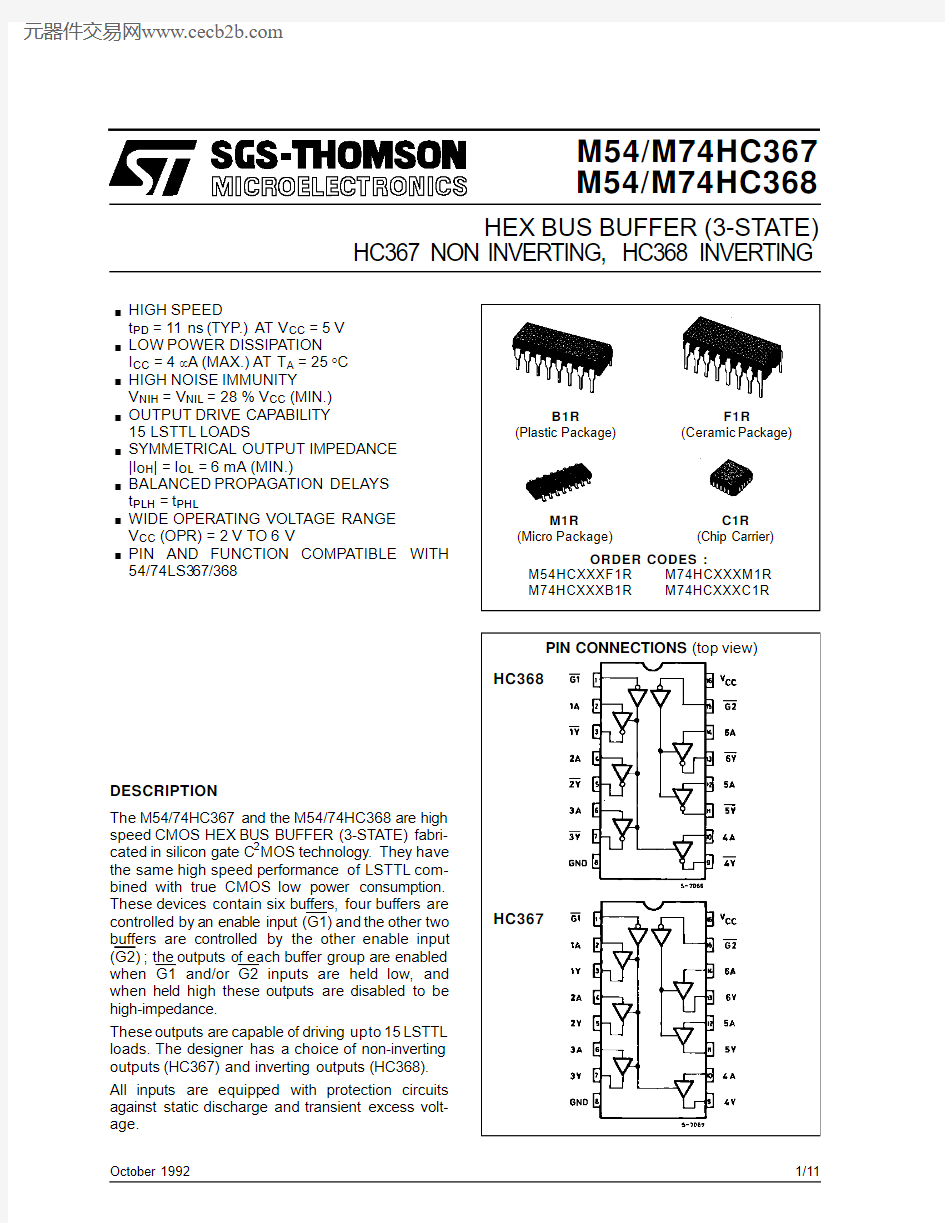
B1R
(Plastic Package)ORDER CODES :
M54HCXXXF1R M74HCXXXM1R M74HCXXXB1R M74HCXXXC1R
F1R
(Ceramic Package)
M1R
(Micro Package)C1R (Chip Carrier)
PIN CONNECTIONS (top view)
HC368
HC367
DESCRIPTION
.HIGH SPEED
t PD =11ns (TYP.)AT V CC =5V .LOW POWER DISSIPATION I CC =4μA (MAX.)AT T A =25°C .HIGH NOISE IMMUNITY
V NIH =V NIL =28%V CC (MIN.).OUTPUT DRIVE CAPABILITY 15LSTTL LOADS
.SYMMETRICAL OUTPUT IMPEDANCE |I OH |=I OL =6mA (MIN.)
.BALANCED PROPAGATION DELAYS t PLH =t PHL
.WIDE OPERATING VOLTAGE RANGE V CC (OPR)=2V TO 6V
.
PIN AND FUNCTION COMPATIBLE WITH 54/74LS367/368
The M54/74HC367and the M54/74HC368are high
speed CMOS HEX BUS BUFFER (3-STATE)fabri-cated in silicon gate C 2MOS technology.They have the same high speed performance of LSTTL com-bined with true CMOS low power consumption.These devices contain six buffers,four buffers are controlled by an enable input (G1)and the other two buffers are controlled by the other enable input (G2);the outputs of each buffer group are enabled when G1and/or G2inputs are held low,and when held high these outputs are disabled to be high-impedance.
These outputs are capable of driving upto 15LSTTL loads.The designer has a choice of non-inverting outputs (HC367)and inverting outputs (HC368).All inputs are equipp ed with protection circuits against static discharge and transient excess volt-age.
1/11
INPUT AND OUTPUT EQUIVALENT CIRCUIT
CHIP CARRIER
NC=No Internal Connection
HC367HC368
PIN DESCRIPTION(HC367)
PIN No SYMBOL NAME AND FUNCTION 1,15G1,G2Output Enable Inputs
2,4,6,10,
12,14
1A to6A Data Inputs
3,5,7,9,
11,13
1Y to6Y Data Outputs
8GND Ground(0V)
16V CC Positive Supply Voltage PIN DESCRIPTION(HC368)
PIN No SYMBOL NAME AND FUNCTION 1,15G1,G2Output Enable Inputs
2,4,6,10,
12,14
1A to6A Data Inputs
3,5,7,9,
11,13
1Y to6Y Data Outputs
8GND Ground(0V)
16V CC Positive Supply Voltage
TRUTH TABLE
INPUTS OUTPUTS
G An Y n(367)Yn(368)
L L L H
L H H L
H X Z Z
X=DON’T CARE Z=HIGH IMPEDANCE
M54/M74HC367/368
2/11
IEC LOGIC SYMBOL
ABSOLUTE MAXIMUM RATINGS
Symbol Parameter
Value Unit V CC
Supply Voltage -0.5to +7V V I DC Input Voltage -0.5to V CC +0.5V V O DC Output Voltage
-0.5to V CC +0.5
V I IK DC Input Diode Current ±20
mA I OK DC Output Diode Current
±20mA I O
DC Output Source Sink Current Per Output Pin ±35mA I CC
or I GND DC V CC or Ground Current ±70mA P D Power Dissipation
500(*)mW
T stg Storage Temperature
-65to +150
o
C T L
Lead Temperature (10sec)
300
o C
Absolute Maximum Ratings are those values beyond whichdamage to the device may occu r.Functiona l ope ration und er these cond ition isnotimplied.(*)500mW:?65o C derate to 300mW by 10mW/o C:65o C to 85o C
RECOMMENDED OPERATING CONDITIONS
Symbol Parameter
Value Unit V CC
Supply Voltage 2to 6V V I Input Voltage
0to V CC V V O Output Voltage
0to V CC V T op Operating Temperature:M54HC Series
M74HC Series -55to +125-40to +85o
C o C
t r ,t f
Input Rise and Fall Time
V CC =2V 0to 1000ns
V CC =4.5V 0to 500V CC =6V
0to 400
HC367
HC368
M54/M74HC367/368
3/11
DC SPECIFICATIONS
Symbol Parameter
Test Conditions Value
Unit V CC
(V)
T A=25o C
54HC and74HC
-40to85o C
74HC
-55to125o C
54HC
Min.Typ.Max.Min.Max.Min.Max.
V IH High Level Input
Voltage 2.0 1.5 1.5 1.5
V 4.5 3.15 3.15 3.15
6.0 4.2 4.2 4.2
V IL Low Level Input
Voltage 2.00.50.50.5
V 4.5 1.35 1.35 1.35
6.0 1.8 1.8 1.8
V OH High Level
Output Voltage 2.0
V I=
V IH
or
V IL
I O=-20μA
1.9
2.0 1.9 1.9
V 4.5 4.4 4.5 4.4 4.4
6.0 5.9 6.0 5.9 5.9
4.5I O=-6.0mA 4.18 4.31 4.13 4.10
6.0I O=-
7.8mA 5.68 5.8 5.63 5.60
V OL Low Level Output
Voltage 2.0
V I=
V IH
or
V IL
I O=20μA
0.00.10.10.1
V 4.50.00.10.10.1
6.00.00.10.10.1
4.5I O=6.0mA0.170.260.330.40
6.0I O=
7.8mA0.180.260.330.40
I I Input Leakage
Current 6.0
V I=V CC or GND±0.1±1±1μA
I OZ3State Output
Off State Current 6.0
V I=V IH or V IL
V O=V CC or GND
±0.5±5±10μA
I CC Quiescent Supply
Current 6.0V I=V CC or GND44080μA
M54/M74HC367/368 4/11
AC ELECTRICAL CHARACTERISTICS(C L=50pF,Input t r=t f=6ns)
Symbol Parameter
Test Conditions Value
Unit V CC
(V)
C L
(pF)
T A=25o C
54HC and74HC
-40to85o C
74HC
-55to125o C
54HC
Min.Typ.Max.Min.Max.Min.Max.
t TLH t THL Output Transition
Time
2.0
50
25607590
ns
4.57121518
6.06101315
t PLH t PHL Propagation
Delay Time
2.0
50
3085105130
ns
4.510172126
6.09141822
2.0
150
42105130160
ns
4.514212632
6.012182227
t PZL t PZH Output Enable
Time
2.0
50R L=1K?
3690115135
ns
4.511182327
6.09152023
2.0
150R L=1K?
49110140165
ns
4.515222833
6.013192428
t PLZ t PHZ Output Disable
Time
2.0
50R L=1K?
3295120145
ns
4.514192429
6.012162025
C IN Input Capacitance5101010pF
C PD(*)Power Dissipation
Capacitance 33
pF
(*)C PD is defined as the value of the IC’s internal equivalent capac itanc e which is calculated from the operating current con sump tion without load. (Refer to Test Circuit).Average operting current can be obtained by the following equ ation.I CC(opr)=C PD?V CC?f IN+I CC/6(per Channel)
TEST CIRCUIT I CC(Opr.)
INPUT WAVEFORM IS THE SAME AS THAT IN CASE OF SWITCHING CHARACTERISTICS TEST.C PD CALCULATION
C P
D is to be calculated with the following
formula by using the measured value of
I CC(opr.)in the test circuit opposite.
C PD=
I CC(opr)
f IN×V CC
In determining the typical value of C PD,a
relatively high frequency of1MHz was ap-
plied to f IN,in order to eliminate any error
caused by the quiescent supply current.
M54/M74HC367/368
5/11
M54/M74HC367/368
SWITCHING CHARACTERISTICS TEST WAVEFORM
GND
V CC Note:Such a logic level shall be applied to each input that the output voltage stays in the appos ite side to the switch connec tion level,when the outp ut is enabl e.
6/11
M54/M74HC367/368 Plastic DIP16(0.25)MECHANICAL DATA
mm inch
DIM.
MIN.TYP.MAX.MIN.TYP.MAX.
a10.510.020
B0.77 1.650.0300.065
b0.50.020
b10.250.010
D200.787
E8.50.335
e 2.540.100
e317.780.700
F7.10.280
I 5.10.201
L 3.30.130
Z 1.270.050
P001C
7/11
M54/M74HC367/368
Ceramic DIP16/1MECHANICAL DATA
mm inch DIM.
MIN.TYP.MAX.MIN.TYP.MAX.
A200.787 B70.276
D 3.30.130
E0.380.015
e317.780.700
F 2.29 2.790.0900.110
G0.40.550.0160.022
H 1.17 1.520.0460.060
L0.220.310.0090.012 M0.51 1.270.0200.050 N10.30.406 P7.88.050.3070.317 Q 5.080.200
P053D 8/11
M54/M74HC367/368 SO16(Narrow)MECHANICAL DATA
mm inch
DIM.
MIN.TYP.MAX.MIN.TYP.MAX.
A 1.750.068
a10.10.20.0040.007
a2 1.650.064
b0.350.460.0130.018
b10.190.250.0070.010
C0.50.019
c145°(typ.)
D9.8100.3850.393
E 5.8 6.20.2280.244
e 1.270.050
e38.890.350
F 3.8 4.00.1490.157
G 4.6 5.30.1810.208
L0.5 1.270.0190.050
M0.620.024
S8°(max.)
P013H
9/11
M54/M74HC367/368
PLCC20MECHANICAL DATA
mm inch DIM.
MIN.TYP.MAX.MIN.TYP.MAX.
A9.7810.030.3850.395 B8.899.040.3500.356
D 4.2 4.570.1650.180
d1 2.540.100
d20.560.022
E7.378.380.2900.330
e 1.270.050
e3 5.080.200
F0.380.015
G0.1010.004 M 1.270.050
M1 1.140.045
P027A 10/11
M54/M74HC367/368 Information furnished is believed to be accurate and reliable.However,SGS-THOMSON Microelectronics assumes no responsability for the consequences of use of such information nor for any infringement of patents or other rights of third parties which may results from its use.No license is granted by implication or otherwise under any patent or patent rights of SGS-THOMSON Microelectronics.Specificationsmentioned in this publication are subject to change without notice.This publication supersedes and replaces all information previously supplied.
SGS-THOMSON Microelectronics products are not authorized for use ascritical components in life support devices or systems without express written approval of SGS-THOMSON Microelectonics.
?1994SGS-THOMSON Microelectronics-All Rights Reserved
SGS-THOMSON Microelectronics GROUP OF COMPANIES
Australia-Brazil-France-Germany-Hong Kong-Italy-Japan-Korea-Malaysia-Malta-Morocco-The Netherlands-
Singapore-Spain-Sweden-Switzerland-Taiwan-Thailand-United Kingdom-U.S.A
11/11