December 2004Revision 21/11
■Adjustable output voltage: 1.24 to 24V ■Several precision @ 25°C ±2%, ±1%, ±0.5% and ±0.25%
■Sink current capability: 0.4 to 100mA
■Industrial temperature range: -40 to +125°C ■
Performances compatible with industry standard TL431
Description
The TS3431 is a programmable shunt voltage reference with guaranteed temperature stability over the entire temperature range of operation (-40 to +125°C). The output voltage may be set to any value between 1.24V and 24V with an external resistor bridge.
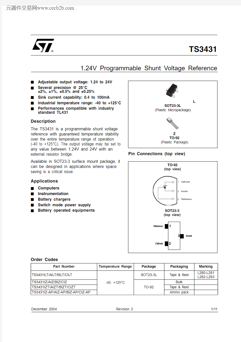
Available in SOT23-3 surface mount package, it can be designed in applications where space saving is a critical issue.
Applications
■Computers
■Instrumentation ■Battery chargers
■Switch mode power supply ■
Battery operated equipments
Pin Connections (top view)
Order Codes
Part Number
Temperature Range
Package Packaging Marking TS3431ILT/AILT/BILT/CILT
-40, +125°C
SOT23-3L
Tape & Reel L280-L281L282-L283
TS3431IZ/AIZ/BIZ/CIZ
TO-92
Bulk TS3431IZT/AIZT/BIZT/CIZT
Tape & Reel TS3431IZ-AP/AIZ-AP/BIZ-AP/CIZ-AP
Ammo pack
TS3431
1.24V Programmable Shunt Voltage Reference
TS3431Absolute Maximum Ratings
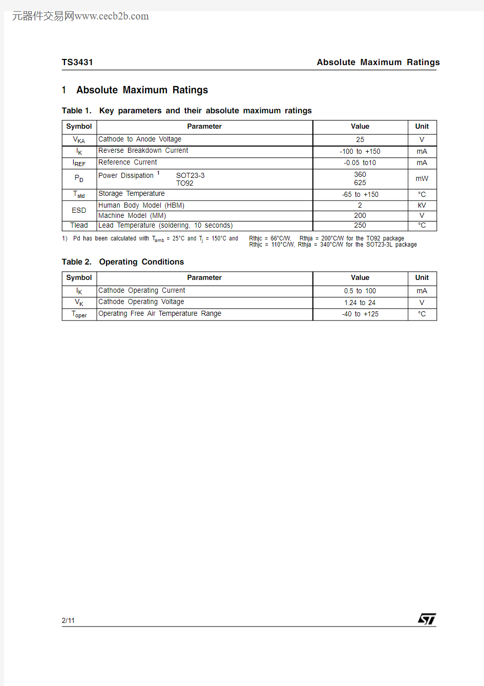
1 Absolute Maximum Ratings
Table 1.Key parameters and their absolute maximum ratings
Symbol Parameter
Value Unit V KA Cathode to Anode Voltage 25V I K Reverse Breakdown Current -100 to +150mA I REF Reference Current -0.05 to10mA P D Power Dissipation 1SOT23-3TO92
1)Pd has been calculated with T amb = 25°C and T j = 150°C and
Rthjc = 66°C/W, Rthja = 200°C/W for the TO92 package
Rthjc = 110°C/W, Rthja = 340°C/W for the SOT23-3L package
360625mW T std Storage Temperature
-65 to +150
°C ESD Human Body Model (HBM)2kV Machine Model (MM)
200V Tlead
Lead Temperature (soldering, 10 seconds)
250
°C
Table 2.Operating Conditions
Symbol Parameter
Value Unit I K Cathode Operating Current 0.5 to 100mA V K Cathode Operating Voltage
1.24 to 24V T oper
Operating Free Air T emperature Range
-40 to +125
°C
2 Electrical Characteristics
Table 3.Tamb = 25°C (unless otherwise specified)
Symbol
Parameter
Test Condition Min.Typ.
Max.Unit
V K
Reference input voltage I K = 10mA
TS3431 (2%) 1.215 1.24 1.265V TS3431A (1%) 1.228 1.252TS3431B (0.5%) 1.234 1.246TS3431C (0.25%)
1.237
1.243?V K
Variation of reference input voltage over temperature 0°C < T < +70°C 10mV -40°C < T < +105°C
18-40°C < T < +125°C
21T C Temperature coefficient -40°C < T < +125°C 100ppm/°C I KMIN
Minimum Operating Current
T = 25°C
0.35
0.4mA -40°C < T < +125°C
0.5Ratio of change in reference input volt-age to change in cathode to anode volt-age
I K =10mA
V K = 24 to 1.24V 1.2 1.5mV/V
-40°C < T < +125°C 2
I REF
Reference input current
I K =10mA, R1=10K ?, R2=+T=25°C
0.9
1.5μA -40°C < T < +125°C 2?I REF
Reference input current deviation I K =10mA, R1=10K ?, R2=+0°C < T < +70°C 0.51μA -40°C < T < +125°C 0.9 1.5I OFF Off-state cathode current V K =24V
T=25°C
35500nA -40°C < T < +105°C 1000-40°C < T < +125°C 2000R KA Reverse Static Impedance I K = 1 to 100mA 0.20.4
?E N
Wideband Noise
I K = 10mA
1kHz < f < 100kHz
100nV/√Hz
Note: Limits are 100% production tested at 25°C. Limits over temperature are guaranteed through correlation and by design.
?Vref ?Vka
---------------∞
Figure 1. Reference voltage vs. temperature
Figure 2. Cathode voltage vs cathode current
Figure 3. Reference input current vs
temperature
Figure 4. Test circuit for V K = Vref
Figure 5. Minimum operating current vs
temperature
Figure 6.
Dynamic impedance vs frequency
Figure 7. Off-State current vs temperature
Figure 8. Ratio of change in reference input
voltage to change in Vka voltage vs temperature
Figure 9. Phase and gain vs frequency
Figure 10. Test circuit for off-state current
measurement
Figure 11. Test circuit for V K > V REF
Figure 12. Test circuit for phase and gain
measurement
Figure 13. Pulse response at Ik=1mA
Figure 14. Pulse response at Ik = 10mA
Figure 15. Block diagram
Figure 16. Test circuit for pulse response at Ik
= 1mA
Figure 17. Test circuit for pulse response at Ik
= 10mA
Figure 18. Equivalent input noise vs
frequency
Package Mechanical Data TS3431
3 Package Mechanical Data
3.1 3 Pins - Plastic Package TO-92 (tape & reel)
https://www.doczj.com/doc/8a13454550.html,limeters
Inches Min.
Typ.
Max.Min.
Typ.
Max.AL
5.00.197A 5.00.197T 4.0
0.157
d 0.45
0.018I1 2.50.098P 11.712.713.70.4610.5000.539PO 12.412.7130.4880.5000.512P2 5.95 6.35 6.750.2340.2500.266F1/F2 2.4 2.5 2.80.0940.0980.110?h -101-0.03900.039?P -101-0.03900.039W 17.518.019.00.6890.7090.748W0 5.76 6.30.2240.2360.248W18.5
9
9.750.3350.354
0.384W20.50.020H 200.787H015.51616.50.6100.6300.650H1250.984DO 3.8
4.0
4.20.150
0.157
0.165L1
11
0.433
TS3431
Package Mechanical Data
3.2 3 Pins - Plastic Package TO-92 (tape ammo pack)
https://www.doczj.com/doc/8a13454550.html,limeters
Inches Min.
Typ.
Max.Min.
Typ.
Max.AL 5.00.197A 5.00.197T 4.0
0.157
d 0.45
0.018I1 2.50.098P 11.712.713.70.4610.5000.539PO 12.412.7130.4880.5000.512P2 5.95 6.35 6.750.2340.2500.266F1/F2 2.4 2.5 2.80.0940.0980.110?h -101-0.03900.039?P -101-0.03900.039W 17.518.019.00.6890.7090.748W0 5.76 6.30.2240.2360.248W18.5
9
9.750.3350.354
0.384W20.50.020H 200.787H015.51616.50.6100.6300.650H1250.984DO 3.8
4.0
4.20.150
0.157
0.165L1
11
0.433
Package Mechanical Data TS3431
TS3431Package Mechanical Data
Revision History TS3431
4 Revision H istory
Date Revision
Description of Changes
01 Jan. 2004
1
First Release
01 Dec. 2004
2
Specific content changes as follows:
?
CI version added in Table:Order Codes on page 1
?Rthjc information added in Table1:Key parameters and their absolute maximum ratings on page 2
?
Test condition added in Table3:Tamb = 25°C (unless o herwise specified) on page 3
Information furnished is believed to be accurate and reliable. However, STMicroelectronics assumes no responsibility for the consequences of use of such information nor for any infringement of patents or other rights of third parties which may result from its use. No license is granted by implication or otherwise under any patent or patent rights of STMicroelectronics. Specifications mentioned in this publication are subject to change without notice. This publication supersedes and replaces all information previously supplied. STMicroelectronics products are not authorized for use as critical components in life support devices or systems without express written approval of STMicroelectronics.
The ST logo is a registered trademark of STMicroelectronics All other names are the property of their respective owners
? 2004 STMicroelectronics - All rights reserved
STMicroelectronics group of companies
Australia - Belgium - Brazil - Canada - China - Czech Republic - Finland - France - Germany - Hong Kong - India - Israel - Italy - Japan -Malaysia - Malta - Morocco - Singapore - Spain - Sweden - Switzerland - United Kingdom - United States of America