
FEATURES
D Routes Any Input to Any Output D Wide Bandwidth: 300 MHz
D Low Crosstalk: –85 dB @ 5 MHz D Double Buffered TTL-Compatible
Latches with Readback
D Low r DS(on): 45
INFORMATION
D Suffix
–40 to 85_C
Max d Unit
8V
90
120
W
SPECIFICATIONS
Parameter Power Supplies Positive Supply Current Negative Supply Current
Matrix Disabled Crosstalk
TIMING DIAGRAMS CS for
Device A
CS for
Device B
Address
B0 – B1
Address
Input
A0 – A3
WR
90%
TEST CIRCUITS
V–
IN1
GND
DGND
A3
WR
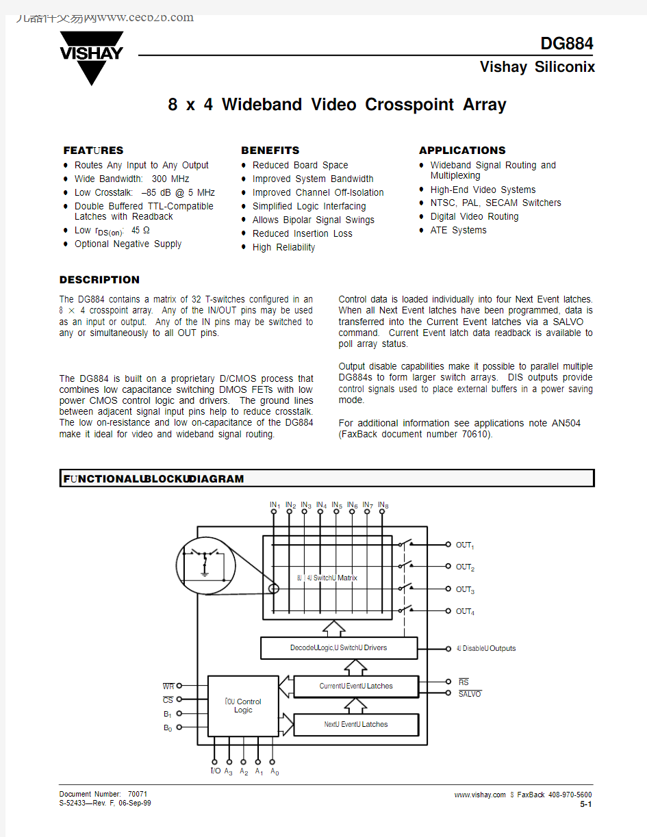
DEVICE DESCRIPTION
Readback
The I/O facility enables the user to write data to the Next Event latches or to read the contents of the Current Event latches. This feature permits the central controller to periodically
APPLICATIONS
A typical switching threshold versus V
These devices feature an address readback facility whereby the last address written to the device may be read by the system. This allows improved status monitoring and hand shaking without additional external components.
When the I/O assigns the address output condition, the A
This datasheet has been download from: https://www.doczj.com/doc/8812069862.html, Datasheets for electronics components.