https://www.doczj.com/doc/8411096980.html, FEATURES
APPLICATIONS
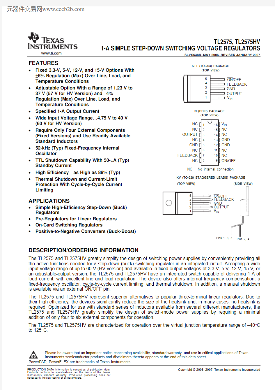
NC
NC
OUTPUT
NC
GND
NC
FEEDBACK
NC
N (PDIP) PACKAGE
(TOP VIEW)
KTT (TO-263) PACKAGE
(TOP VIEW)
1
2
3
4
5
G
N
D
ON/OFF
FEEDBACK
GND
OUTPUT
V IN
FEEDBACK
KV (TO-220 STAGGERED LEADS) PACKAGE (TOP VIEW)(SIDE VIEW)
Pins 1, 3, 5Pins 2, 4
DESCRIPTION/ORDERING INFORMATION TL2575,TL2575HV
1-A SIMPLE STEP-DOWN SWITCHING VOLTAGE REGULATORS
SLVS638B–MAY2006–REVISED JANUARY2007?Fixed3.3-V,5-V,12-V,and15-V Options With
±5%Regulation(Max)Over Line,Load,and
Temperature Conditions
?Adjustable Option With a Range of1.23V to
37V(57V for HV Version)and±4%
Regulation(Max)Over Line,Load,and
Temperature Conditions
?Specified1-A Output Current
?Wide Input Voltage Range…4.75V to40V
(60V for HV Version)
?Require Only Four External Components
(Fixed Versions)and Use Readily Available
Standard Inductors
?52-kHz(Typ)Fixed-Frequency Internal
Oscillator
?TTL Shutdown Capability With50-μA(Typ)
Standby Current
?High Efficiency…as High as88%(Typ)
?Thermal Shutdown and Current-Limit
Protection With Cycle-by-Cycle Current
Limiting
?Simple High-Efficiency Step-Down(Buck)
Regulators
?Pre-Regulators for Linear Regulators
?On-Card Switching Regulators
?Positive-to-Negative Converters(Buck-Boost)
The TL2575and TL2575HV greatly simplify the design of switching power supplies by conveniently providing all the active functions needed for a step-down(buck)switching regulator in an integrated circuit.Accepting a wide input voltage range of up to60V(HV version)and available in fixed output voltages of3.3V,5V,12V,15V,or an adjustable-output version,the TL2575and TL2575HV have an integrated switch capable of delivering1A of load current,with excellent line and load regulation.The device also offers internal frequency compensation,a fixed-frequency oscillator,cycle-by-cycle current limiting,and thermal shutdown.In addition,a manual shutdown is available via an external ON/OFF pin.
The TL2575and TL2575HV represent superior alternatives to popular three-terminal linear regulators.Due to their high efficiency,the devices significantly reduce the size of the heatsink and,in many cases,no heatsink is required.Optimized for use with standard series of inductors available from several different manufacturers,the TL2575and TL2575HV greatly simplify the design of switch-mode power supplies by requiring a minimal addition of only four to six external components for operation.
The TL2575and TL2575HV are characterized for operation over the virtual junction temperature range of–40°C to125°C.
Please be aware that an important notice concerning availability,standard warranty,and use in critical applications of Texas
Instruments semiconductor products and disclaimers thereto appears at the end of this data sheet.
https://www.doczj.com/doc/8411096980.html,
TL2575,TL2575HV
1-A SIMPLE STEP-DOWN SWITCHING VOLTAGE REGULATORS
SLVS638B–MAY 2006–REVISED JANUARY 2007
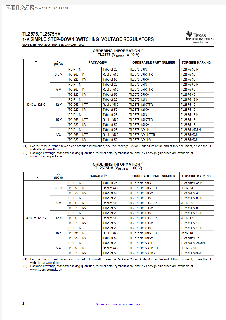
ORDERING INFORMATION (1)
TL2575(V IN(MAX)=40V)
V O T J
PACKAGE (2)
ORDERABLE PART NUMBER TOP-SIDE MARKING (NOM)
PDIP –N
Tube of 25TL2575-33IN TL2575-33IN 3.3V
TO-263–KTT Reel of 500TL2575-33IKTTR TL2575-33I TO-220–KV Tube of 50TL2575-33IKV TL2575-33I PDIP –N
Tube of 25TL2575-05IN TL2575-05IN 5V
TO-263–KTT Reel of 500TL2575-05IKTTR TL2575-05I TO-220–KV Tube of 50TL2575-05IKV TL2575-05I PDIP –N
Tube of 25TL2575-12IN TL2575-12IN –40°C to 125°C
12V
TO-263–KTT Reel of 500TL2575-12IKTTR TL2575-12I TO-220–KV Tube of 50TL2575-12IKV TL2575-12I PDIP –N
Tube of 25TL2575-15IN TL2575-15IN 15V
TO-263–KTT Reel of 500TL2575-15IKTTR TL2575-15I TO-220–KV Tube of 50TL2575-15IKV TL2575-15I PDIP –N
Tube of 25TL2575-ADJIN TL2575-ADJIN ADJ
TO-263–KTT Reel of 500TL2575-ADJIKTTR TL2575ADJI TO-220–KV
Tube of 50
TL2575-ADJIKV
TL2575ADJI
(1)For the most current package and ordering information,see the Package Option Addendum at the end of this document,or see the TI web site at https://www.doczj.com/doc/8411096980.html,.
(2)
Package drawings,standard packing quantities,thermal data,symbolization,and PCB design guidelines are available at https://www.doczj.com/doc/8411096980.html,/sc/package.
ORDERING INFORMATION (1)TL2575HV (V IN(MAX)=60V)
V O T J
PACKAGE (2)
ORDERABLE PART NUMBER TOP-SIDE MARKING (NOM)
PDIP –N
Tube of 25TL2575HV-33IN TL2575HV-33IN 3.3V
TO-263–KTT Reel of 500TL2575HV-33IKTTR 2BHV-33I TO-220–KV Tube of 50TL2575HV-33IKV TL2575HV-33I PDIP –N
Tube of 25TL2575HV-05IN TL2575HV-05IN 5V
TO-263–KTT Reel of 500TL2575HV-05IKTTR 2BHV-05I TO-220–KV Tube of 50TL2575HV-05IKV TL2575HV-05I PDIP –N
Tube of 25TL2575HV-12IN TL2575HV-12IN –40°C to 125°C
12V
TO-263–KTT Reel of 500TL2575HV-12IKTTR 2BHV-12I TO-220–KV Tube of 50TL2575HV-12IKV TL2575HV-12I PDIP –N
Tube of 25TL2575HV-15IN TL2575HV-15IN 15V
TO-263–KTT Reel of 500TL2575HV-15IKTTR 2BHV-15I TO-220–KV Tube of 50TL2575HV-15IKV TL2575HV-15I PDIP –N
Tube of 25TL2575HV-ADJIN TL2575HV-ADJIN ADJ
TO-263–KTT Reel of 500TL2575HV-ADJIKTTR 2BHV-ADJI TO-220–KV
Tube of 50
TL2575HV-ADJIKV
TL2575HVADJI
(1)For the most current package and ordering information,see the Package Option Addendum at the end of this document,or see the TI web site at https://www.doczj.com/doc/8411096980.html,.
(2)
Package drawings,standard packing quantities,thermal data,symbolization,and PCB design guidelines are available at https://www.doczj.com/doc/8411096980.html,/sc/package.
https://www.doczj.com/doc/8411096980.html,
Unregulated
DC Input
5 V: R2 = 3.1 k W 12 V: R2 = 8.84 k W 15 V: R2 = 11.3 k W
ADJ: R1 = Open, R2 = 0 ?
7-V to 40-V Unregulated
DC Input
5-V
Regulated Output 1-A Load
TL2575,TL2575HV
1-A SIMPLE STEP-DOWN SWITCHING VOLTAGE REGULATORS
SLVS638B–MAY 2006–REVISED JANUARY 2007
FUNCTIONAL BLOCK DIAGRAM
A.Pin numbers are for the KTT (TO-263)package.
A.Pin numbers are for the KTT (TO-263)package.
Figure 1.Typical Application Circuit (Fixed Version)
https://www.doczj.com/doc/8411096980.html,
Absolute Maximum Ratings (1)
Package Thermal Data (1)
Recommended Operating Conditions
TL2575,TL2575HV
1-A SIMPLE STEP-DOWN SWITCHING VOLTAGE REGULATORS
SLVS638B–MAY 2006–REVISED JANUARY 2007
over operating free-air temperature range (unless otherwise noted)
MIN
MAX UNIT TL2575HV 60V IN
Supply voltage
V TL2575
42ON/OFF input voltage range –0.3
V IN V Output voltage to GND (steady state)
–1V T J Maximum junction temperature 150°C T stg Storage temperature range
–65
150
°C
(1)
Stresses beyond those listed under absolute maximum ratings may cause permanent damage to the device.These are stress ratings only,and functional operation of the device at these or any other conditions beyond those indicated under recommended operating conditions is not implied.Exposure to absolute-maximum-rated conditions for extended periods may affect device reliability.
PACKAGE BOARD θJA θJC θJP (2)
PDIP (N)High K,JESD 51-767°C/W 57°C/W TO-263(KTT)High K,JESD 51-526.5°C/W 31.8°C/W 0.38°C/W TO-220(KV)
High K,JESD 51-5
26.5°C/W
31.8°C/W
0.38°C/W (1)Maximum power dissipation is a function of T J (max),θJA ,and T A .The maximum allowable power dissipation at any allowable ambient temperature is P D =(T J (max)–T A )/θJA .Operating at the absolute maximum T J of 150°C can affect reliability.
(2)
For packages with exposed thermal pads,such as QFN,PowerPAD?,or PowerFLEX?,θJP is defined as the thermal resistance between the die junction and the bottom of the exposed pad.
MIN
MAX UNIT TL2575HV 4.7560V IN Supply voltage
V TL2575
4.7540T J
Operating virtual junction temperature
–40
125
°C
https://www.doczj.com/doc/8411096980.html,
TL2575Electrical Characteristics TL2575,TL2575HV
1-A SIMPLE STEP-DOWN SWITCHING VOLTAGE REGULATORS
SLVS638B–MAY2006–REVISED JANUARY2007
I LOAD =200mA,V
IN
=12V for3.3-V,5-V,and adjustable versions,V
IN
=25V for12-V version,V
IN
=30V for15-V version
(unless otherwise noted)(see Figure2)
TL2575
PARAMETER TEST CONDITIONS T J UNIT
MIN TYP MAX
V IN=12V,I LOAD=0.2A25°C 3.234 3.3 3.366
TL2575-3325°C 3.168 3.3 3.432
4.75V≤V IN≤40V,
0.2A≤I LOAD≤1A Full range 3.135 3.465
V IN=12V,I LOAD=0.2A25°C 4.95 5.1
TL2575-0525°C 4.85 5.2
8V≤V IN≤40V,
0.2A≤I LOAD≤1A Full range 4.75 5.25
V OUT Output voltage V
V IN=25V,I LOAD=0.2A25°C11.761212.24
TL2575-1225°C11.521212.48
15V≤V IN≤40V,
0.2A≤I LOAD≤1A Full range11.412.6
V IN=30V,I LOAD=0.2A25°C14.71515.3
TL2575-1525°C14.41515.6
18V≤V IN≤40V,
0.2A≤I LOAD≤1A Full range14.251515.75
V IN=12V,V OUT=5V,
25°C 1.217 1.23 1.243
I LOAD=0.2A
Feedback voltage TL2575-ADJ V
25°C 1.193 1.23 1.267
8V≤V IN≤40V,V OUT=5V,
0.2A≤I LOAD≤1A Full range 1.18 1.28
TL2575-33V IN=12V,I LOAD=1A75
TL2575-05V IN=12V,I LOAD=1A77
TL2575-12V IN=15V,I LOAD=1A88
ηEfficiency25°C%
TL2575-15V IN=18V,I LOAD=1A88
V IN=12V,V OUT=5V,
TL2575-ADJ77
I LOAD=1A
25°C50100
I IB Feedback bias current V OUT=5V(ADJ version only)nA
Full range500
25°C475258
f o Oscillator frequency(1)kHz
Full range4263
25°C0.9 1.2
V SAT Saturation voltage I OUT=1A(2)V
Full range 1.4 Maximum duty cycle(3)25°C9398%
25°C 1.7 2.8 3.6
I CL Switch peak current(1)(2)A
Full range 1.34
V IN=40(4),Output=0V2
I L Output leakage current25°C mA
V IN=40(4),Output=–1V7.530
I Q Quiescent current(4)25°C510mA
I STBY Standby quiescent current OFF(ON/OFF=5V)25°C50200μA
(1)In the event of an output short or an overload condition,self-protection features lower the oscillator frequency to~18kHz and the
minimum duty cycle from5%to~2%.The resulting output voltage drops to~40%of its nominal value,causing the average power dissipated by the IC to lower.
(2)Output is not connected to diode,inductor,or capacitor.Output is sourcing current.
(3)FEEDBACK is disconnected from output and connected to0V.
(4)To force the output transistor off,FEEDBACK is disconnected from output and connected to12V for the adjustable,3.3-V,and5-V
versions and to25V for the12-V and15-V versions.
https://www.doczj.com/doc/8411096980.html,
TL2575,TL2575HV
1-A SIMPLE STEP-DOWN SWITCHING VOLTAGE REGULATORS
SLVS638B–MAY 2006–REVISED JANUARY 2007
TL2575Electrical Characteristics (continued)
I LOAD =200mA,V IN =12V for 3.3-V,5-V,and adjustable versions,V IN =25V for 12-V version,V IN =30V for 15-V version (unless otherwise noted)(see Figure 2)
TL2575PARAMETER
TEST CONDITIONS
T J UNIT MIN TYP MAX
25°C 2.2 1.4
ON/OFF high-level logic V IH OFF (V OUT =0V)
V input voltage
Full range 2.4
25°C 1.2
1ON/OFF low-level logic V IL ON (V OUT =nominal voltage)V input voltage
Full range 0.8I IH ON/OFF high-level input current OFF (ON/OFF =5V)25°C 1230μA I IL
ON/OFF low-level input current
ON (ON/OFF =0V)
25°C
10
μA
https://www.doczj.com/doc/8411096980.html,
TL2575HV Electrical Characteristics TL2575,TL2575HV
1-A SIMPLE STEP-DOWN SWITCHING VOLTAGE REGULATORS
SLVS638B–MAY2006–REVISED JANUARY2007
I LOAD =200mA,V
IN
=12V for3.3-V,5-V,and adjustable versions,V
IN
=25V for12-V version,V
IN
=30V for15-V version
(unless otherwise noted)(see Figure2)
TL2575HV
PARAMETER TEST CONDITIONS T J UNIT
MIN TYP MAX
V IN=12V,I LOAD=0.2A25°C 3.234 3.3 3.366
TL2575HV-3325°C 3.168 3.3 3.450
4.75V≤V IN≤60V,
0.2A≤I LOAD≤1A Full range 3.135 3.482
V IN=12V,I LOAD=0.2A25°C 4.95 5.1
TL2575HV-0525°C 4.85 5.225
8V≤V IN≤60V,
0.2A≤I LOAD≤1A Full range 4.75 5.275
V OUT Output voltage V
V IN=25V,I LOAD=0.2A25°C11.761212.24
TL2575HV-1225°C11.521212.54
15V≤V IN≤60V,
0.2A≤I LOAD≤1A Full range11.412.66
V IN=30V,I LOAD=0.2A25°C14.71515.3
TL2575HV-1525°C14.41515.68
18V≤V IN≤60V,
0.2A≤I LOAD≤1A Full range14.251515.83
V IN=12V,V OUT=5V,
25°C 1.217 1.23 1.243
I LOAD=0.2A
Feedback voltage TL2575HV-ADJ V
25°C 1.193 1.23 1.273
8V≤V IN≤60V,V OUT=5V,
0.2A≤I LOAD≤1A Full range 1.180 1.286
TL2575HV-33V IN=12V,I LOAD=1A75
TL2575HV-05V IN=12V,I LOAD=1A77
TL2575HV-12V IN=15V,I LOAD=1A88
ηEfficiency25°C% TL2575HV-15V IN=18V,I LOAD=1A88
V IN=12V,V OUT=5V,
TL2575HV-ADJ77
I LOAD=1A
25°C50100
I IB Feedback bias current V OUT=5V(ADJ version only)nA
Full range500
25°C475258
f o Oscillator frequency(1)kHz
Full range4263
25°C0.9 1.2
V SAT Saturation voltage I OUT=1A(2)V
Full range 1.4 Maximum duty cycle(3)25°C9398%
25°C 1.7 2.8 3.6
I CL Switch peak current(1)(2)A
Full range 1.34
V IN=60(4),Output=0V2
I L Output leakage current25°C mA
V IN=60(4),Output=–1V7.530
I Q Quiescent current(4)25°C510mA
I STBY Standby quiescent current OFF(ON/OFF=5V)25°C50200μA
(1)In the event of an output short or an overload condition,self-protection features lower the oscillator frequency to~18kHz and the
minimum duty cycle from5%to~2%.The resulting output voltage drops to~40%of its nominal value,causing the average power dissipated by the IC to lower.
(2)Output is not connected to diode,inductor,or capacitor.Output is sourcing current.
(3)FEEDBACK is disconnected from output and connected to0V.
(4)To force the output transistor off,FEEDBACK is disconnected from output and connected to12V for the adjustable,3.3-V,and5-V
versions and to25V for the12-V and15-V versions.
https://www.doczj.com/doc/8411096980.html,
TL2575,TL2575HV
1-A SIMPLE STEP-DOWN SWITCHING VOLTAGE REGULATORS
SLVS638B–MAY 2006–REVISED JANUARY 2007
TL2575HV Electrical Characteristics (continued)
I LOAD =200mA,V IN =12V for 3.3-V,5-V,and adjustable versions,V IN =25V for 12-V version,V IN =30V for 15-V version (unless otherwise noted)(see Figure 2)
TL2575HV PARAMETER
TEST CONDITIONS T J UNIT MIN TYP MAX
25°C 2.2 1.4
ON/OFF high-level logic V IH OFF (V OUT =0V)
V input voltage
Full range 2.4
25°C 1.2
1V IL ON/OFF low-level logic input voltage ON (V OUT =nominal voltage)V Full range 0.8I IH ON/OFF high-level input current OFF (ON/OFF =5V)1230μA 25°C
I IL
ON/OFF low-level input current
ON (ON/OFF =0V)
10
μA
https://www.doczj.com/doc/8411096980.html,
TEST CIRCUITS
C IN = 100 μF , Aluminum Electrolytic C OUT = 330 μF , Aluminum Electrolytic D1 = Schottky
L1 = 330 μH (for 5-V V IN with 3.3-V V OUT , use 100 m H)
Fixed-Output Voltage
Adjustable-Output Voltage
V OUT = V REF (1 + R2/R1) = 5 V V REF = 1.23 V R1 = 2 k W R2 = 6.12 k W
TL2575,TL2575HV
1-A SIMPLE STEP-DOWN SWITCHING VOLTAGE REGULATORS
SLVS638B–MAY 2006–REVISED JANUARY 2007
A.Pin numbers are for the KTT (TO-263)package.
Figure 2.Test Circuits and Layout Guidelines
https://www.doczj.com/doc/8411096980.html,
TYPICAL CHARACTERISTICS
-0.6
-0.4-0.200.20.40.60.811.21.40102030405060
V IN –Input Voltage –V
O u t p u t V o l t a g e C h a n g e –
%
-1-0.8-0.6-0.4-0.200.20.40.60.81-50
-250255075100125150
T A –Temperature –°C
O u t p u t V o l t a g e C h a n g e –
%
0.25
0.50.75
11.251.5
1.752-40-25-10
5203550658095110125
T J –Junction Temperature –°C
I n p u t -O u t p u t D i f f e r e n t i a l –V
00.5
1
1.5
2
2.53
-50
-250255075100125150
T J –Junction Temperature –°C
I O –O u t p u t C u r r e n t –A
TL2575,TL2575HV
1-A SIMPLE STEP-DOWN SWITCHING VOLTAGE REGULATORS
SLVS638B–MAY 2006–REVISED JANUARY 2007
Figure 3.Normalized Output Voltage Figure 4.Line Regulation
Figure 5.Dropout Voltage Figure 6.Current Limit
https://www.doczj.com/doc/8411096980.html,
02468101214161820
10
20
30
40
50
60
V IN –Input Voltage –V
I Q –Q u i e s c e n t C u r r e n t –m A
050100150200250300350400450500-50
-250255075100125150
T J –Junction Temperature –°C
I S T B Y –S t a n d b y Q u i e s c e n t C u r r e n t –
μA
-10-8-6-4-20246
8
10-50
-250255075100125150
T J –Junction Temperature –°C
f N O R M –N o r m a l i z e d F r e
q u e n c y –%
0.4
0.5
0.6
0.70.8
0.911.1
1.20
0.2
0.4
0.6
0.8
1
I SW –Switch Current –A
V S A T –S a t u r a t i o n
V o l t a g e –V
TL2575,TL2575HV
1-A SIMPLE STEP-DOWN SWITCHING VOLTAGE REGULATORS
SLVS638B–MAY 2006–REVISED JANUARY 2007
TYPICAL CHARACTERISTICS (continued)
Figure 7.Quiescent Current Figure 8.Standby Quiescent Current
Figure 9.Oscillator Frequency Figure 10.Switch Saturation Voltage
-50
-250
255075100125
150
T J –Junction Temperature –°C -50
-25
25
50
75
100
125
150
T J –Junction Temperature –°C
D
B
{
0 A
C
0 A
{
A
0V
{
V = 5V
OUT 4 μs/Div
Figure 11.Minimum Operating Voltage
Figure 12.FEEDBACK Current
A.Output pin voltage,10V/Div
B.Output pin current,1A/Div
C.Inductor current,0.5A/Div
D.
Ouput ripple voltage,20mV/Div
Figure 13.Switching Waveforms
https://www.doczj.com/doc/8411096980.html,
00.20.40.60.811.2
1.41.6-0.1
00.10.20.30.40.50.60.70.80.9
t –Time –ms
I L O A D –L o a d C u r r e n t –
A
TL2575,TL2575HV
1-A SIMPLE STEP-DOWN SWITCHING VOLTAGE REGULATORS
SLVS638B–MAY 2006–REVISED JANUARY 2007
TYPICAL CHARACTERISTICS (continued)
Figure 14.Load Transient Response
https://www.doczj.com/doc/8411096980.html,
APPLICATION INFORMATION
Input Capacitor (C IN )
Output Capacitor (C OUT )
Catch Diode
TL2575,TL2575HV
1-A SIMPLE STEP-DOWN SWITCHING VOLTAGE REGULATORS
SLVS638B–MAY 2006–REVISED JANUARY 2007
For stability concerns,an input bypass capacitor (electrolytic,C IN ≥47μF)needs to be located as close as possible to the regulator.For operating temperatures below –25°C,C IN may need to be larger in value.In addition,since most electrolytic capacitors have decreasing capacitances and increasing ESR as temperature drops,adding a ceramic or solid tantalum capacitor in parallel increases the stability in cold temperatures.To extend the capacitor operating lifetime,the capacitor RMS ripple current rating should be:I C,RMS > 1.2(t on /T)I LOAD where
t on /T =V OUT /V IN {buck regulator}and
t on /T =|V OUT |/(|V OUT |+V IN ){buck-boost regulator}
For both loop stability and filtering of ripple voltage,an output capacitor also is required,again in close proximity to the regulator.For best performance,low-ESR aluminum electrolytics are recommended,although standard aluminum electrolytics may be adequate for some applications.Based on the following equation:Output ripple voltage =(ESR of C OUT )×(inductor ripple current)
Output ripple of 50mV to 150mV typically can be achieved with capacitor values of 220μF to 680μhttps://www.doczj.com/doc/8411096980.html,rger C OUT can reduce the ripple 20mV to 50mV peak to peak.To improve further on output ripple,paralleling of standard electrolytic capacitors may be used.Alternatively,higher-grade capacitors such as high frequency,low inductance,or low ESR can be used.
The following should be taken into account when selecting C OUT :
?At cold temperatures,the ESR of the electrolytic capacitors can rise dramatically (typically 3×nominal value at –25°C).Because solid tantalum capacitors have significantly better ESR specifications at cold temperatures,they should be used at operating temperature lower than –25°C.As an alternative,tantalums also can be paralleled to aluminum electrolytics and should contribute 10%to 20%to the total capacitance.?Low ESR for C OUT is desirable for low output ripple.However,the ESR should be greater than 0.05?to avoid the possibility of regulator instability.Hence,a sole tantalum capacitor used for C OUT is most susceptible to this occurrence.
?The capacitor’s ripple current rating of 52kHz should be at least 50%higher than the peak-to-peak inductor ripple current.
As with other external components,the catch diode should be placed close to the output to minimize unwanted noise.Schottky diodes have fast switching speeds and low forward voltage drops and,thus,offer the best performance,especially for switching regulators with low output voltages (V OUT <5V).If a high-efficiency,fast-recovery,or ultra-fast-recovery diode is used in place of a Schottky,it should have a soft recovery (versus abrupt turn-off characteristics)to avoid the chance of causing instability and EMI.Standard 50-/60-Hz diodes,such as the 1N4001or 1N5400series,are not suitable.
https://www.doczj.com/doc/8411096980.html,
Inductor
Output Voltage Ripple and Transients
Feedback Connection
ON/OFF Input TL2575,TL2575HV
1-A SIMPLE STEP-DOWN SWITCHING VOLTAGE REGULATORS
SLVS638B–MAY2006–REVISED JANUARY2007
APPLICATION INFORMATION(continued)
Proper inductor selection is key to the performance-switching power-supply designs.One important factor to consider is whether the regulator is used in continuous mode(inductor current flows continuously and never drops to zero)or in discontinuous mode(inductor current goes to zero during the normal switching cycle).Each mode has distinctively different operating characteristics and,therefore,can affect the regulator performance and requirements.In many applications,the continuous mode is the preferred mode of operation,since it offers greater output power with lower peak currents,and also can result in lower output ripple voltage.The advantages of continuous mode of operation come at the expense of a larger inductor required to keep inductor current continuous,especially at low output currents and/or high input voltages.
The TL2575and TL2575HV can operate in either continuous or discontinuous mode.With heavy load currents, the inductor current flows continuously and the regulator operates in continuous mode.Under light load,the inductor fully discharges and the regulator is forced into the discontinuous mode of operation.For light loads (approximately200mA or less),this discontinuous mode of operation is perfectly acceptable and may be desirable solely to keep the inductor value and size small.Any buck regulator eventually operates in discontinuous mode when the load current is light enough.
The type of inductor chosen can have advantages and disadvantages.If high performance/quality is a concern, then more-expensive toroid core inductors are the best choice,as the magnetic flux is contained completely within the core,resulting in less EMI and noise in nearby sensitive circuits.Inexpensive bobbin core inductors, however,generate more EMI as the open core does not confine the flux within the core.Multiple switching regulators located in proximity to each other are particularly susceptible to mutual coupling of magnetic fluxes from each other’s open cores.In these situations,closed magnetic structures(such as a toroid,pot core,or E-core)are more appropriate.
Regardless of the type and value of inductor used,the inductor never should carry more than its rated current. Doing so may cause the inductor to saturate,in which case the inductance quickly drops,and the inductor looks like a low-value resistor(from the dc resistance of the windings).As a result,switching current rises dramatically (until limited by the current-by-current limiting feature of the TL2575and TL2575HV)and can result in overheating of the inductor and the IC itself.Note that different types of inductors have different saturation characteristics.
As with any switching power supply,the output of the TL2575and TL2575HV have a sawtooth ripple voltage at the switching frequency.Typically about1%of the output voltage,this ripple is due mainly to the inductor sawtooth ripple current and the ESR of the output capacitor(see note on C OUT).Furthermore,the output also may contain small voltage spikes at the peaks of the sawtooth waveform.This is due to the fast switching of the output switch and the parasitic inductance of C OUT.These voltage spikes can be minimized through the use of low-inductance capacitors.
There are several ways to reduce the output ripple voltage:a larger inductor,a larger C OUT,or both.Another method is to use a small LC filter(20μH and100μF)at the output.This filter can reduce the output ripple voltage by a factor of10(see Figure2).
For fixed-voltage options,FEEDBACK must be wired to V OUT.For the adjustable version,FEEDBACK must be connected between the two programming resistors.Again,both of these resistors should be in close proximity to the regulator,and each should be less than100k?to minimize noise pickup.
ON/OFF should be grounded or be a low-level TTL voltage(typically<1.6V)for normal operation.To shut down the TL2575or TL2575HV and put it in standby mode,a high-level TTL or CMOS voltage should be supplied to this pin.ON/OFF should not be left open and safely can be pulled up to V IN with or without a pullup resistor.
https://www.doczj.com/doc/8411096980.html,
Grounding
Layout Guidelines
TL2575,TL2575HV
1-A SIMPLE STEP-DOWN SWITCHING VOLTAGE REGULATORS
SLVS638B–MAY 2006–REVISED JANUARY 2007
APPLICATION INFORMATION (continued)
The power and ground connections of the TL2575and TL2575HV must be low impedance to help maintain output stability.For the 5-pin packages,both pin 3and tab are ground,and either connection can be used as they are both part of the same lead frame.With the 16-pin package,all the ground pins (including signal and power grounds)should be soldered directly to wide PCB copper traces to ensure low-inductance connections and good thermal dissipation.
With any switching regulator,circuit layout plays an important role in circuit performance.Wiring and parasitic inductances,as well as stray capacitances,are subjected to rapidly switching currents,which can result in unwanted voltage transients.To minimize inductance and ground loops,the length of the leads indicated by heavy lines should be minimized.Optimal results can be achieved by single-point grounding (see Figure 2)or by ground-plane construction.For the same reasons,the two programming resistors used in the adjustable version should be located as close as possible to the regulator to keep the sensitive feedback wiring short.
https://www.doczj.com/doc/8411096980.html,
BUCK REGULATOR DESIGN PROCEDURE TL2575,TL2575HV
1-A SIMPLE STEP-DOWN SWITCHING VOLTAGE REGULATORS
SLVS638B–MAY2006–REVISED JANUARY2007
PROCEDURE(Fixed Output)EXAMPLE(Fixed Output)
Known:Known:
V OUT=3.3V,5V,12V,or15V V OUT=5V
V IN(Max)=Maximum input voltage V IN(Max)=20V
I LOAD(Max)=Maximum load current I LOAD(Max)=1A
1.Inductor Selection(L1) 1.Inductor Selection(L1)
A.From Figure15through Figure18,select the appropriate inductor A.From Figure16(TL2575-05),the intersection of20-V line and code based on the intersection of V IN(Max)and I LOAD(Max).1-A line gives an inductor code of L330.
B.From Table2,choose the appropriate inductor based on the B.L330→L1=330μH
inductor code.Parts from three well-known inductor manufacturers Choose from:
are given.The inductor chosen should be rated for operation at
34042(Schott)
52-kHz and have a current rating of at least1.15×I LOAD(Max)to
PE-52627(Pulse Engineering)
allow for the ripple current.The actual peak current in L1(in normal
operation)can be calculated as follows:RL1952(Renco)
I L1(pk)=I LOAD(Max)+(V IN–V OUT)×t on/2L1
Where t on=V OUT/V IN×(1/f osc)
2.Output Capacitor Selection(C OUT) 2.Output Capacitor Selection(C OUT)
A.The TL2575control loop has a two-pole two-zero frequency A.C OUT=100-μF to470-μF,standard aluminum electrolytic response.The dominant pole-zero pair is established by C OUT and
L1.To meet stability requirements while maintaining an acceptable
output ripple voltage(V ripple≈0.01×V OUT),the recommended range
for a standard aluminum electrolytic C OUT is between100μF and
470μF.
B.C OUT should have a voltage rating of at least1.5×V OUT.But if a B.Although a C OUT rated at8V is sufficient for V OUT=5V,a
low output ripple voltage is desired,choose capacitors with a higher-voltage capacitor is chosen for its typically lower ESR(and higher-voltage ratings than the minimum required,due to their hence lower output ripple voltage)→Capacitor voltage
typically lower ESRs.rating=20V.
3.Catch Diode Selection(D1)(see Table1) 3.Catch Diode Selection(D1)(see Table1)
A.In normal operation,the catch diode requires a current rating of A.Pick a diode with3-A rating.
at least1.2×I LOAD(Max).For the most robust design,D1should be
rated to handle a current equal to the TL2575maximum switch peak
current;this represents the worst-case scenario of a continuous
short at V OUT.
B.The diode requires a reverse voltage rating of at least B.Pick30-V rated Schottky diode(1N5821,MBR330,31QD03,or
1.25×V IN(Max).SR303)or100-V rated Fast Recovery diode(31DF1,MURD310,or
HER302).
4.Input Capacitor(C IN) 4.Input Capacitor(C IN)
An aluminum electrolytic or tantalum capacitor is needed for input C IN=100μF,25V,aluminum electrolytic
bypassing.Locate C IN as close to the V IN and GND pins as
possible.
https://www.doczj.com/doc/8411096980.html,
(
TL2575,TL2575HV
1-A SIMPLE STEP-DOWN SWITCHING VOLTAGE REGULATORS
SLVS638B–MAY 2006–REVISED JANUARY 2007
元器件交易网https://www.doczj.com/doc/8411096980.html,
https://www.doczj.com/doc/8411096980.html,
Inductor Value Selection Guide for Continuous-Mode
Operation
TL2575,TL2575HV
1-A SIMPLE STEP-DOWN SWITCHING VOLTAGE REGULATORS
SLVS638B–MAY 2006–REVISED JANUARY 2007
Figure 15.TL2575-33Figure 16.TL2575-50
Figure 17.TL2575-12Figure 18.TL2575-15
Figure 19.TL2575-ADJ
https://www.doczj.com/doc/8411096980.html,
TL2575,TL2575HV
1-A SIMPLE STEP-DOWN SWITCHING VOLTAGE REGULATORS
SLVS638B–MAY 2006–REVISED JANUARY 2007
Table 1.Diode Selection Guide
SCHOTTKY
FAST RECOVERY
V R 1A 3A 1A
3A
1N58171N582020V
MBR120P MBR320SR102SR3021N58181N5821MBR130P MBR33030V
11DQ0331DQ03SR103SR303The following diodes The following diodes 1N5819IN5822are all rated to 100V:are all rated to 100V:
MBR140P MBR34011DF131DF140V
11DQ0431DQ04MUR110MURD310SR104SR304HER102HER302
MBR150MBR35050V
11DQ0531DQ05SR105SR305MBR160MBR36060V
11DQ0631DQ06SR106
SR306
Table 2.Inductor Selection by Manufacturer's Part Number
INDUCTOR VALUE
SCHOTT
RENCO
INDUCTOR CODE
PULSE ENGINEERING (2)
(μH)
CORPORATION (1)
ELECTRONICS (3)
L10010067127000PE-92108RL2444L15015067127010PE-53113RL1954L22022067127020PE-52626RL1953L33033067127030PE-52627RL1952L47047067127040PE-53114RL1951L68068067127050PE-52629RL1950H15015067127060PE-53115RL2445H22022067127070PE-53116RL2446H33033067127080PE-53117RL2447H47047067127090PE-53118RL1961H68068067127100PE-53119RL1960H1000100067127110PE-53120RL1959H1500150067127120PE-53121RL1958H2200
2200
67127130
PE-53122
RL2448
(1)
Schott Corporation,(612)475-1173,1000Parkers Lake Rd.,Wayzata,MN 55391(2)Pulse Engineering,(619)674-8100,P.O.Box 12236,San Diego,CA 92112
(3)
Renco Electronics Inc.,(516)586-5566,60Jeffryn Blvd.East,Deer Park,NY 11729