LC420WUL
Product Specification
SPECIFICATION FOR APPROVAL
(
) Preliminary Specification
( ● ) Final Specification
Title
BUYER MODEL General
42.0” WUXGA TFT LCD
SUPPLIER *MODEL SUFFIX LG Display Co., Ltd. LC420WUL SBT1(RoHS Verified)
*When you obtain standard approval, please use the above model name without suffix SIGNATURE DATE
APPROVED BY /
APPROVED BY
SIGNATURE DATE
P.Y. Kim /Team Leader
REVIEWED BY
/
S.K. Park / Project Leader
PREPARED BY
/
Y.S. Kim / Engineer
Please return 1 copy for your confirmation with your signature and comments.
Ver. 0.1
TV Product Development Dept. LG Display Co., Ltd.
1 /40
LC420WUL
Product Specification
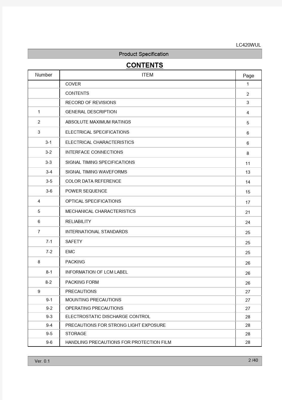
CONTENTS
Number
COVER CONTENTS RECORD OF REVISIONS 1 2 3 3-1 3-2 3-3 3-4 3-5 3-6 4 5 6 7 7-1 7-2 8 8-1 8-2 9 9-1 9-2 9-3 9-4 9-5 9-6 GENERAL DESCRIPTION ABSOLUTE MAXIMUM RATINGS ELECTRICAL SPECIFICATIONS ELECTRICAL CHARACTERISTICS INTERFACE CONNECTIONS SIGNAL TIMING SPECIFICATIONS SIGNAL TIMING WAVEFORMS COLOR DATA REFERENCE POWER SEQUENCE OPTICAL SPECIFICATIONS MECHANICAL CHARACTERISTICS RELIABILITY INTERNATIONAL STANDARDS SAFETY EMC PACKING INFORMATION OF LCM LABEL PACKING FORM PRECAUTIONS MOUNTING PRECAUTIONS OPERATING PRECAUTIONS ELECTROSTATIC DISCHARGE CONTROL PRECAUTIONS FOR STRONG LIGHT EXPOSURE STORAGE HANDLING PRECAUTIONS FOR PROTECTION FILM
ITEM
Page
1 2 3 4 5 6 6 8 11 13 14 15 17 21 24 25 25 25 26 26 26 27 27 27 28 28 28 28
Ver. 0.1
2 /40
LC420WUL
Product Specification
RECORD OF REVISIONS
Revision No.
0.0 0.1
Revision Date
June 03, 2009 August 04, 2009
Page
7 16 34,35 4 6 7 10 17 18 23 24
Description
Preliminary Specification (First Draft) Power Consumption, PWM frequency Driver Off Sequence changed Option pin Block Diagram changed Power Consumption (logic), ELECTRICAL CHARACTERISTICS Notes 2 delete Notes 5 impedance register value key-in Color Coordinates Backlight aging time 2Hr Rear View Shock test 1Hr
1.0
September,4,2009
7 22 23 26 31 33 40
Final Specification Lift Time FRONT View Changed REAR VIEW Changed Packing Form Changed Pallet Ass’y Changed
Pallet Label Changed
Updated TBD items
Ver. 0.1
3 /40
LC420WUL
Product Specification
1. General Description
The LC420WUL is a Color Active Matrix Liquid Crystal Display with an integral Light Emitting Diode (LED) backlight system. The matrix employs a-Si Thin Film Transistor as the active element. It is a transmissive display type which is operating in the normally black mode. It has a 42.02 inch diagonally measured active display area with WUXGA resolution (1080 vertical by 1920 horizontal pixel array). Each pixel is divided into Red, Green and Blue sub-pixels or dots which are arrayed in vertical stripes. Gray scale or the luminance of the sub-pixel color is determined with a 10-bit gray scale signal for each dot. Therefore, it can present a palette of more than 1.06B(FRC) colors. It has been designed to apply the 10-bit 4-port LVDS interface. It is intended to support LCD TV, PCTV where high brightness, super wide viewing angle, high color gamut, high color depth and fast response time are important.
CN2 LVDS
(41pin)
Mini-LVDS(RGB) EEPROM SCL SDA
G1 S1
Source Driver Circuit
S1920
2Port
LVDS 3,4 +12.0V LVDS
Gate Driver Circuit
(51pin)
CN1 LVDS 1,2
Timing Controller
[LVDS Rx + OPC + ODC integrated]
2Port
LVDS Select Bit Select OPC Enable ExtVBR-B OPC out +24.0V, GND, On/Off ExtVBR-B I2C Option signal
TFT - LCD Panel
(1920 × RGB × 1080 pixels)
G1080
Power Circuit Block
LED Driver
Back light Assembly
General Features
Active Screen Size Outline Dimension Pixel Pitch Pixel Format Color Depth Luminance, White Viewing Angle (CR>10) Power Consumption Weight Display Mode Surface Treatment 42.02 inches(1067.31mm) diagonal 973.2(H) × 566.2(V) X 11.9(B)/25.5 mm(D) (Typ.) 0.4845 mm x 0.4845 mm 1920 horiz. by 1080 vert. Pixels, RGB stripe arrangement 10-bit(D), 1.06 B colors 450 cd/m2 (Center 1point ,Typ.) Viewing angle free ( R/L 178 (Min.), U/D 178 (Min.)) Total 119.5W [Logic= 6.5W, LED Driver=113W (ExtVbr_B=100% )] 10.3 Kg (Typ.) Transmissive mode, Normally black Hard coating(3H), Anti-glare treatment of the front polarizer (Haze 10%) 4 /40
Ver. 0.1
LC420WUL
Product Specification
2. Absolute Maximum Ratings
The following items are maximum values which, if exceeded, may cause faulty operation or damage to the LCD module.
Table 1. ABSOLUTE MAXIMUM RATINGS Parameter
Power Input Voltage LCM Backlight LED Driver
Symbol
VLCD VBL VON/OFF VBR TOP TST HOP HST
Value Min
-0.3 -0.3 -0.3 0 0 -20 10 10
Max
+14.0 +27.0 +5.5 +5.0 +50 +60 90 90
Unit
VDC VDC VDC VDC
Remark
at 25 ± 2 °C
ON/OFF Control Voltage Brightness Control Voltage Operating Temperature Storage Temperature Operating Ambient Humidity Storage Humidity
°C °C
Note 1,2 %RH %RH
Notes : 1. Temperature and relative humidity range are shown in the figure below. Wet bulb temperature should be Max 39 °C and no condensation of water. 2. Gravity mura can be guaranteed below 40℃ condition.
90% 60 60% Humidity [(%)RH] 50 Wet Bulb Temperature [°C] 40 40% 30 20 10 0 10% 10 20 30 40 50 60 70 80 Storage
Operation
-20
0
Dry Bulb Temperature [°C]
Ver. 0.1
5 /40
LC420WUL
Product Specification
3. Electrical Specifications 3-1. Electrical Characteristics
It requires two power inputs. One is employed to power for the LCD circuit. The other Is used for the LED backlight and LED driver circuit. Table 2. ELECTRICAL CHARACTERISTICS Value Parameter
Circuit : Power Input Voltage Power Input Current Power Consumption Rush current VLCD ILCD PLCD IRUSH 737 6.5 958 8.45 3.0 mA Watt A 2 1 3 10.8 12.0 542 13.2 704 VDC mA 1
Symbol Min Typ Max
Unit
Note
Notes : 1. The specified current and power consumption are under the VLCD=12.0V, 25 ± 2°C, fV=120Hz condition whereas mosaic pattern(8 x 6) is displayed and fV is the frame frequency. 2. The current is specified at the maximum current pattern. 3. The duration of rush current is about 2ms and rising time of power input is 0.5ms (min.).
White : 1023Gray Black : 0Gray
Mosaic Pattern(8 x 6)
Ver. 0.1
6 /40
LC420WUL
Product Specification
Table 3. ELECTRICAL CHARACTERISTICS (Continue)
Values Parameter LED Driver : Power Supply Input Voltage Power Supply Input Current VBL IBL_A 22.8 24.0 4.7 25.2 5.4 Vdc A 1 Ext VBR-B = 100% 1 Ext VBR-B = 100% 4 Ext VBR-B = 100% Symbol Min Typ Max Unit Notes
Power Supply Input Current (In-Rush) Power Consumption On On/Off Off Input Voltage for Control System Signals Brightness Adjust PWM Frequency for NTSC & PAL Pulse Duty Level (PWM) LED : Life Time
Irush PBL V on V off ExtVBR-B PAL NTSC High Level Low Level
2.5 -0.3 10 2.5 0.0
113.0 0.0 100 120 -
8.5
130
A W Vdc Vdc % Hz Hz
5.0 0.8 100
On Duty 3 3 HIGH : on duty LOW : off duty
5.0 0.8
Vdc Vdc
30,000
-
Hrs
2
Notes : 1. Electrical characteristics are determined after the unit has been ‘ON’ and stable for approximately 120 minutes at 25±2°C. The specified current and power consumption are under the typical supply Input voltage 24Vand VBR (ExtVBR-B : 100%), it is total power consumption. 2. The life time(MTTF) is determined as the time which luminance of the LED is 50% compared to that of initial value at the typical LED current (ExtVBR-B :100%) on condition of continuous operating in LCM state at 25±2°C. 3. LGD recommend that the PWM freq. is synchronized with One time harmonic of Vsync signal of system. Though PWM frequency is over 120Hz (max 252Hz), function of LED Driver is not affected. 4. The duration of rush current is about 10ms. 5. Even though inrush current is over the specified value, there is no problem if I2T spec of fuse is satisfied.
Ver. 0.1
7 /40
LC420WUL
Product Specification
3-2. Interface Connections
This LCD module employs two kinds of interface connection, 51-pin and 41-pin connector are used for the module electronics and Master 14-pin connector is used for the integral backlight system. 3-2-1. LCD Module - LCD Connector(CN1): FI-R51S-HF(manufactured by JAE) or KN25-51P-0.5SH(manufactured by Hirose) Refer to below and next Page table - Mating Connector : FI-R51HL(JAE) or compatible Table 4-1. MODULE CONNECTOR(CN1) PIN CONFIGURATION
No 1 2 3 4 5 6 7 8 9 10 11 12 13 14 15 16 17 18 19 20 21 22 23 24 25 26 Symbol NC NC NC NC NC NC LVDS Select VBR EXT OPC OUT OPC Enable GND R1AN R1AP R1BN R1BP R1CN R1CP GND R1CLKN R1CLKP GND R1DN R1DP R1EN R1EP Reserved Description No Connection No Connection No Connection No Connection No Connection No Connection ‘H’ =JEIDA , ‘L’ or NC = VESA External VBR (From System) OPC output (From LCM) ‘H’ = Enable , ‘L’ or NC = Disable Ground FIRST LVDS Receiver Signal (A-) FIRST LVDS Receiver Signal (A+) FIRST LVDS Receiver Signal (B-) FIRST LVDS Receiver Signal (B+) FIRST LVDS Receiver Signal (C-) FIRST LVDS Receiver Signal (C+) Ground FIRST LVDS Receiver Clock Signal(-) FIRST LVDS Receiver Clock Signal(+) Ground FIRST LVDS Receiver Signal (D-) FIRST LVDS Receiver Signal (D+) FIRST LVDS Receiver Signal (E-) FIRST LVDS Receiver Signal (E+) No connection or GND No 27 28 29 30 31 32 33 34 35 36 37 38 39 40 41 42 43 44 45 46 47 48 49 50 51 Symbol Bit Select R2AN R2AP R2BN R2BP R2CN R2CP GND R2CLKN R2CLKP GND R2DN R2DP R2EN R2EP Reserved Reserved GND GND GND NC VLCD VLCD VLCD VLCD Description ‘H’ or NC= 10bit(D) , ‘L’ = 8bit SECOND LVDS Receiver Signal (A-) SECOND LVDS Receiver Signal (A+) SECOND LVDS Receiver Signal (B-) SECOND LVDS Receiver Signal (B+) SECOND LVDS Receiver Signal (C-) SECOND LVDS Receiver Signal (C+) Ground SECOND LVDS Receiver Clock Signal(-) SECOND LVDS Receiver Clock Signal(+) Ground SECOND LVDS Receiver Signal (D-) SECOND LVDS Receiver Signal (D+) SECOND LVDS Receiver Signal (E-) SECOND LVDS Receiver Signal (E+) No connection or GND No connection or GND Ground Ground Ground No connection Power Supply +12.0V Power Supply +12.0V Power Supply +12.0V Power Supply +12.0V -
Notes : 1. All GND(ground) pins should be connected together to the LCD module’s metal frame. 2. All VLCD (power input) pins should be connected together. 3. All Input levels of LVDS signals are based on the EIA 644 Standard. (Please see the Appendix X) 4. Specific pins(pin No. #2~#6) are used for internal data process of the LCD module. If not used, these pins are no connection. 5. Specific pins(pin No. #8~#10) are used for OPC function of the LCD module. If not used, these pins are no connection. (Please see the Appendix V for more information.) 6. LVDS pin (pin No. #24,25,40,41) are used for 10Bit(D) of the LCD module. If used for 8Bit(R), these pins are no connection. 7. Specific pin No. #44 is used for “No signal detection” of system signal interface. It should be GND for NSB(No Signal Black) during the system interface signal is not. If this pin is “H”, LCD Module displays AGP(Auto Generation Pattern).
Ver. 0.1 8 /40
LC420WUL
Product Specification
- LCD Connector(CN2): FI-RE41S-HF, Refer to below table - Mating Connector : FI-RE41HL Table 4-2. MODULE CONNECTOR(CN2) PIN CONFIGURATION
No
1 2 3 4 5 6 7 8 9 10 11 12 13 14 15 16 17 18 19 20 21
Symbol
NC NC NC NC NC NC NC NC GND RA3N RA3P RB3N RB3P RC3N RC3P GND RCLK3N RCLK3P GND RD3N RD3P
Description
No connection(Reserved) No connection No connection No connection No connection No connection No connection No connection Ground THIRD LVDS Receiver Signal (A-) THIRD LVDS Receiver Signal (A+) THIRD LVDS Receiver Signal (B-) THIRD LVDS Receiver Signal (B+) THIRD LVDS Receiver Signal (C-) THIRD LVDS Receiver Signal (C+) Ground THIRD LVDS Receiver Clock Signal(-) THIRD LVDS Receiver Clock Signal(+) Ground THIRD LVDS Receiver Signal (D-) THIRD LVDS Receiver Signal (D+)
No
22 23 24 25 26 27 28 29 30 31 32 33 34 35 36 37 38 39 40 41 -
Symbol
RE3N RE3P GND GND RA4N RA4P RB4N RB4P RC4N RC4P GND RCLK4N RCLK4P GND RD4N RD4P RE4N RE4P GND GND
Description
THIRD LVDS Receiver Signal (E-) THIRD LVDS Receiver Signal (E+) Ground Ground FOURTH LVDS Receiver Signal (A-) FOURTH LVDS Receiver Signal (A+) FOURTH LVDS Receiver Signal (B-) FOURTH LVDS Receiver Signal (B+) FOURTH LVDS Receiver Signal (C-) FOURTH LVDS Receiver Signal (C+) Ground FOURTH LVDS Receiver Clock Signal(-) FOURTH LVDS Receiver Clock Signal(+) Ground FOURTH LVDS Receiver Signal (D-) FOURTH LVDS Receiver Signal (D+) FOURTH LVDS Receiver Signal (E-) FOURTH LVDS Receiver Signal (E+) Ground Ground
Notes : 1. All GND(ground) pins should be connected together to the LCD module’s metal frame. 2. LVDS pin (pin No. #22,23,38,39) are used for 10Bit(D) of the LCD module. If used for 8Bit(R), these pins are no connection. [CN1] -Part/No. : FI-RE51S-HF(JAE) KN25-51P-0.5SH(Hirose) - Mating connector : FI-RE51HL (Manufactured by JAE) [CN2] - Part/No. : FI-RE41S-HF(JAE) - Mating connector : FI-RE41HL (Manufactured by JAE)
#1
CN1
#51
#1
CN2
#41
#1
#51
#1
#41
Rear view of LCM
Ver. 0.1
9 /40
LC420WUL
Product Specification
3-2-2. Backlight LED DRIVER Master - LED Driver Connector : 20022WR-14B1(Yeonho) or Equivalent - Mating Connector : 20022HS-14 or Equivalent Table 5. LED DRIVER CONNECTOR PIN CONFIGURATION Pin No 1 2 3 4 5 6 7 8 9 10 11 12 13 14 Symbol
VBL VBL VBL VBL VBL GND GND GND GND GND VBR-A VON/OFF EXTVBR-B GND
Description
Power Supply +24.0V Power Supply +24.0V Power Supply +24.0V Power Supply +24.0V Power Supply +24.0V Backlight Ground Backlight Ground Backlight Ground Backlight Ground Backlight Ground N.C Backlight ON/OFF control External PWM Backlight Ground
Master
VBL VBL VBL VBL VBL GND GND GND GND GND OPEN or GND VON/OFF EXTVBR-B GND
Note
1
2 3
Notes : 1. GND should be connected to the LCD module’s metal frame. 2. ON : 2.5 ~ 5.0V / OFF : 0.0 ~ 0.8V . Open or ‘H’ for B/L On is default status. 3. High : on duty / Low : off duty, Pin#13 can be opened. ( if Pin #13 is open , EXTVBR-B is 100% ) 4. #14 of Input CNT Must be Connected to Backlight Ground. 5. Each impedance of pin #12 and 13 is 40 [K?] and 10 [K?]. ◆ Rear view of LCM PCB 14 … … 1
10 /40
Ver. 0.1
LC420WUL
Product Specification
3-3. Signal Timing Specifications
Table 6 shows the signal timing required at the input of the LVDS transmitter. All of the interface signal timing should be satisfied with the following specification for normal operation.
Table 6. TIMING TABLE for NTSC/ATSC (DE Only Mode) ITEM Display Period Horizontal Blank Total Display Period Vertical Blank Total Symbol Min 480 40 520 1080 10 1090 Typ 480 70 550 1080 45 1125 Max 480 200 680 1080 86 1166 Unit Note 1920/4 1
tHV tHB tHP tVV tVB tVP
Symbol
tCLK tCLK tCLK
Lines Lines Lines
1
ITEM DCLK Frequency Horizontal Vertical
Min 66.97 121.8 108.2
Typ 74.25 135 120
Max 75 136.4 121.2
Unit
Note
fCLK fH fV
MHz KHz Hz
2 2
Notes : 1. The Input of HSYNC & VSYNC signal does not have an effect on normal operation(DE Only Mode). If you use spread spectrum for EMI, add some additional clock to minimum value for clock margin. 2. The performance of the electro-optical characteristics may be influenced by variance of the vertical refresh rate and the horizontal frequency.
Ver. 0.1
11 /40
LC420WUL
Product Specification
Table 7 shows the signal timing required at the input of the LVDS transmitter. All of the interface signal timing should be satisfied with the following specification for normal operation.
Table7. TIMING TABLE for DVB/PAL (DE Only Mode) ITEM Display Period Horizontal Blank Total Display Period Vertical Blank Total Symbol Min 480 40 520 1080 228 1308 Typ 480 70 550 1080 270 1350 Max 480 200 680 1080 300 1380 Unit Note 1920/4 1
tHV tHB tHP tVV tVB tVP
Symbol
tCLK tCLK tCLK
Lines Lines Lines
1
ITEM DCLK Frequency Horizontal Vertical
Min 66.97 121.8 95
Typ 74.25 135 100
Max 75 136.4 103.7
Unit
Note
fCLK fH fV
MHz KHz Hz
2 2
Notes : 1. The Input of HSYNC & VSYNC signal does not have an effect on normal operation(DE Only Mode). If you use spread spectrum for EMI, add some additional clock to minimum value for clock margin. 2. The performance of the electro-optical characteristics may be influenced by variance of the vertical refresh rate and the horizontal frequency.
Ver. 0.1
12 /40
LC420WUL
Product Specification
3-4. Signal Timing Waveforms
DE, Data 0.7VDD 0.3VDD DCLK
tCLK
0.5 VDD
Valid data First data
Invalid data
Pixel 0
Pixel 4
Invalid data
Valid data Second data
Invalid data
Pixel 1
Pixel 5
Invalid data
Valid data Third data
Invalid data
Pixel 2
Pixel 6
Invalid data
Valid data Forth data
Invalid data
Pixel 3
Pixel 7
Invalid data
DE(Data Enable) * tHB = tHFP + tWH +tHBP
* Reference : Sync. Relation
tHP HSync tWH tHBP tHV
* tVB = tVFP + tWV +tVBP
tHFP
DE(Data Enable) tVP tWV VSync tVBP tVV tVFP
DE(Data Enable)
Ver. 0.1
13 /40
LC420WUL
Product Specification
3-5. Color Data Reference
The brightness of each primary color(red,green,blue) is based on the 10-bit gray scale data input for the color. The higher binary input, the brighter the color. Table 8 provides a reference for color versus data input. Table 8. COLOR DATA REFERENCE
Input Color Data Color RED MSB LSB MSB GREEN LSB MSB BLUE LSB
R9 R8 R7 R6 R5 R4 R3 R2 R1 R0
G9 G8 G7 G6 G5 G4 G3 G2 G1 G0 0 0 0 0 0 0 0 0 0 0 0 0 0 0 0 0 0 0 0 0 1 1 1 1 1 1 1 1 1 1 0 0 0 0 0 0 0 0 0 0 1 1 1 1 1 1 1 1 1 1 0 0 0 0 0 0 0 0 0 0 1 1 1 1 1 1 1 1 1 1 1 1 1 1 1 1 1 1 1 1 0 0 0 0 0 0 0 0 0 0 0 0 0 0 0 0 0 0 0 0 ... 0 0 0 0 0 0 0 0 0 0 0 0 0 0 0 0 0 0 0 0 0 0 0 0 0 0 0 0 0 0 0 0 0 0 0 0 0 0 0 1 ... 1 1 1 1 1 1 1 1 1 0 1 1 1 1 1 1 1 1 1 1 0 0 0 0 0 0 0 0 0 0 0 0 0 0 0 0 0 0 0 0 ... 0 0 0 0 0 0 0 0 0 0 0 0 0 0 0 0 0 0 0 0
B9 B8 B7 B6 B5 B4 B3 B2 B1 B0 0 0 0 0 0 0 0 0 0 0 0 0 0 0 0 0 0 0 0 0 0 0 0 0 0 0 0 0 0 0 1 1 1 1 1 1 1 1 1 1 1 1 1 1 1 1 1 1 1 1 1 1 1 1 1 1 1 1 1 1 0 0 0 0 0 0 0 0 0 0 1 1 1 1 1 1 1 1 1 1 0 0 0 0 0 0 0 0 0 0 0 0 0 0 0 0 0 0 0 0 ... 0 0 0 0 0 0 0 0 0 0 0 0 0 0 0 0 0 0 0 0 0 0 0 0 0 0 0 0 0 0 0 0 0 0 0 0 0 0 0 0 ... 0 0 0 0 0 0 0 0 0 0 0 0 0 0 0 0 0 0 0 0 0 0 0 0 0 0 0 0 0 0 0 0 0 0 0 0 0 0 0 1 ... 1 1 1 1 1 1 1 1 1 0 1 1 1 1 1 1 1 1 1 1
Black Red (1023) Green (1023) Basic Color Blue (1023) Cyan Magenta Yellow White RED (000) RED (001) RED ... RED (1022) RED (1023) GREEN (000) GREEN (001) GREEN ... GREEN (1022) GREEN (1023) BLUE (000) BLUE (001) BLUE ... BLUE (1022) BLUE (1023)
0 0 0 0 0 0 0 0 0 0 1 1 1 1 1 1 1 1 1 1 0 0 0 0 0 0 0 0 0 0 0 0 0 0 0 0 0 0 0 0 0 0 0 0 0 0 0 0 0 0 1 1 1 1 1 1 1 1 1 1 1 1 1 1 1 1 1 1 1 1 1 1 1 1 1 1 1 1 1 1 0 0 0 0 0 0 0 0 0 0 0 0 0 0 0 0 0 0 0 1 ... 1 1 1 1 1 1 1 1 1 0 1 1 1 1 1 1 1 1 1 1 0 0 0 0 0 0 0 0 0 0 0 0 0 0 0 0 0 0 0 0 ... 0 0 0 0 0 0 0 0 0 0 0 0 0 0 0 0 0 0 0 0 0 0 0 0 0 0 0 0 0 0 0 0 0 0 0 0 0 0 0 0 ... 0 0 0 0 0 0 0 0 0 0 0 0 0 0 0 0 0 0 0 0
Ver. 0.1
14 /40
LC420WUL
Product Specification
3-6. Power Sequence
3-6-1. LCD Driving circuit
90% 50% 10% T1 T2
Power Supply For LCD VLCD
0V
10%
T6
Valid Data
Invalid Data Invalid Data
Interface Signal (Tx_clock)
30% 0V
100% T7
T3
T4
User Control Signal (LVDS_select, BIT_select) Power for LED LED ON
Table 9. POWER SEQUENCE
Parameter T1 T2 T3 T4 T6 T7 Value Min 0.5 0 200 200 1.0 0 Typ Max 20 T2 Unit ms ms ms ms s ms 4 3 3 5 4 Notes
Note :1. Please avoid floating state of interface signal at invalid period. 2. When the power supply for LCD (VLCD) is off, be sure to pull down the valid and invalid data to 0V. 3. The T3/T4 is recommended value, the case when failed to meet a minimum specification, abnormal display would be shown. There is no reliability problem. 4. If the on time of signals(Interface signal and user control signals) precedes the on time of Power(VLCD), it will be happened abnormal display. When T7 is NC status, T7 doesn’t need to be measured. 5. T6 should be measured after the Module has been fully discharged between power off and on period.
Ver. 0.1
15 /40
LC420WUL
Product Specification
3-6-2. Sequence for LED Driver Power Supply For LED Driver
24V (typ.) 90%
VBL
10% 0V 0.7V
T1
T2
T3
VON/OFF
LED BL ON
Ext-VBR-B
T4 T5
3-6-3. Dip condition for LED Driver
T8 VBL : 24V
VBL(Typ.) x 0.8
0V Table 10. Power Sequence for LED Driver
Parameter T1 T2 T3 T4 T5 T8 Values Min 20 500 10 0 0 Typ Max 10 Units ms ms ms ms ms ms VBL(Typ) x 0.8 Remarks 1
Notes : 1. T1 describes rising time of 0V to 24V and this parameter does not applied at restarting time. Even though T1 is over the specified value, there is no problem if I2T spec of fuse is satisfied.
Ver. 0.1
16 /40
LC420WUL
Product Specification
4. Optical Specification
Optical characteristics are determined after the unit has been ‘ON’ and stable in a dark environment at 25±2°C. The values specified are at an approximate distance 50cm from the LCD surface at a viewing angle of Φ and θ equal to 0 °. FIG. 1 shows additional information concerning the measurement equipment and method. LCD Module Pritchard 880 or equivalent
Optical Stage(x,y)
50cm FIG. 1 Optical Characteristic Measurement Equipment and Method Table 11. OPTICAL CHARACTERISTICS Parameter
Contrast Ratio Surface Luminance, white Luminance Variation Gray-to-Gray MPRT Uniformity Uniformity RED GREEN Color Coordinates [CIE1931] BLUE WHITE Viewing Angle (CR>10) x axis, right(φ=0°) x axis, left (φ=180°) y axis, up (φ=90°) y axis, down (φ=270°) Gray Scale Ver. 0.1 θr θl θu θd 89 89 89 89 8 17 /40 degree 7 Ta= 25±2°C, VLCD=12.0V, fV=120Hz, Dclk =74.25MHz VBR_A=1.65V, EXTVBR-B=100%
Symbol
CR LWH δ WHITE G to G MPRT δ MPRT δ G TO G Rx Ry Gx Gy Bx By Wx Wy 5P
Value Min
900 360 -
Typ
1300 450 5 8 0.640 0.331 0.282
Max
1.3 8 12 1 1
Unit
Note
1
cd/m2 ms ms
2 3 4 5 6 6
Response Time
Typ -0.03
0.634 0.151 0.057 0.279 0.292
Typ +0.03
LC420WUL
Product Specification
Notes :1. Contrast Ratio(CR) is defined mathematically as : CR(Contrast Ratio) = Maximum CRn (n=1, 2, 3, 4, 5) Surface Luminance at position n with all white pixels CR = Surface Luminance at position n with all black pixels n = the Position number(1, 2, 3, 4, 5). For more information, see FIG 2. 2. Surface luminance are determined after the unit has been ‘ON’ and 1Hour after lighting the backlight in a dark environment at 25±2°C. Surface luminance is the luminance value at center 1-point across the LCD surface 50cm from the surface with all pixels displaying white. For more information see the FIG. 2. 3. The variation in surface luminance , δ WHITE is defined as : δ WHITE(5P) = Maximum(Lon1,Lon2, Lon3, Lon4, Lon5) / Minimum(Lon1,Lon2, Lon3, Lon4, Lon5) Where Lon1 to Lon5 are the luminance with all pixels displaying white at 5 locations . For more information, see the FIG. 2. 4. Response time is the time required for the display to transition from G(N) to G(M) (Rise Time, TrR) and from G(M) to G(N) (Decay Time, TrD). For additional information see the FIG. 3. (N
LC420WUL
Product Specification
Measuring point for surface luminance & measuring point for luminance variation.
H A
② ①
B V
③
④
⑤
A : H / 4 mm B : V / 4 mm @ H,V : Active Area
FIG. 2 5 Points for Luminance Measure
Response time is defined as the following figure and shall be measured by switching the input signal for “Gray(N)” and “Gray(M)”.
T rR 100 90
T rD
Optical Response
10 0 Gray(N) Gray(M) N,M = Black~White, N
19 /40
LC420WUL
Product Specification
MPRT is defined as the 10% to 90% blur-edge with Bij(pixels) and scroll speed U(pixels/frame)at the moving picture.
M=
1 U
Lj
Bij (i=j)
90%
Example) Bij = 12pixels, U = 10pixels / 120Hz M = 12pixels / (10pixels / 120Hz) = 12pixels / {10pixels / (1/120)s} i = 12 / 1,200 s = 10 ms FIG. 4 MPRT
L
10%
Bij
Dimension of viewing angle range
Normal E Y φ = 90 ° , Up
φ = 180 ° , Left
θ φ
φ = 0 ° , Right
φ = 270 ° , Down
FIG. 5 Viewing Angle
Ver. 0.1 20 /40