1/10
August 2001s
HIGH SPEED : f MAX = 48MHz (TYP.) at V CC = 4.5V s
LOW POWER DISSIPATION:I CC =2μA(MAX.) at T A =25°C
s
COMPATIBLE WITH TTL OUTPUTS : V IH = 2V (MIN.) V IL = 0.8V (MAX)
s
BALANCED PROPAGATION DELAYS:t PLH ? t PHL
s
SYMMETRICAL OUTPUT IMPEDANCE:|I OH | = I OL = 4mA (MIN)
s
PIN AND FUNCTION COMPATIBLE WITH 74 SERIES 74
DESCRIPTION
The M74HCT74 is an high speed CMOS DUAL D TYPE FLIP FLOP WITH CLEAR fabricated with silicon gate C 2MOS technology.
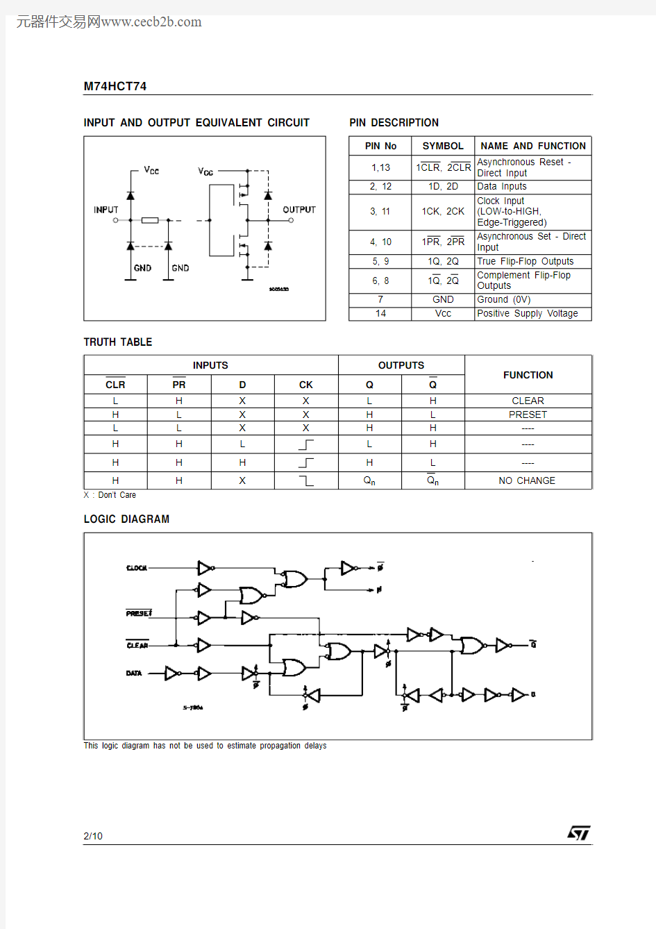
A signal on the D INPUT (nD) is transferred on the Q OUTPUT during the positive going transition of the clock pulse. CLEAR (CLR) and PRESET (PR)are independent of the clock and accomplished by a low on the appropriate input.
The M74HCT74 is designed to directly interface HSC 2MOS systems with TTL and NMOS components.
All inputs are equipped with protection circuits against static discharge and transient excess voltage.
M74HCT74
DUAL D TYPE FLIP FLOP WITH PRESET AND CLEAR
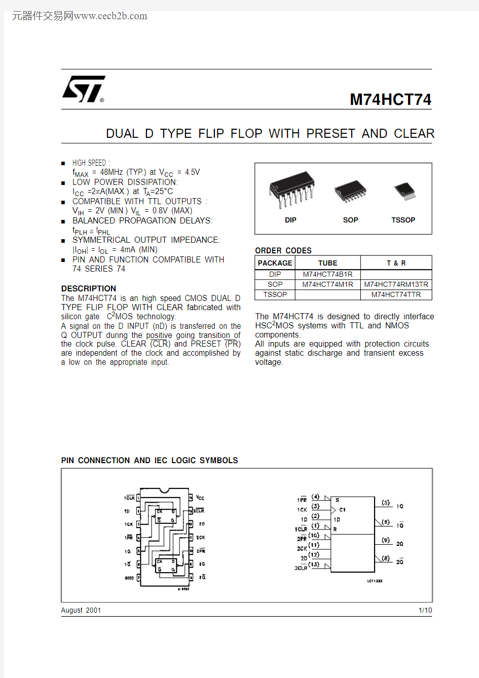
PIN CONNECTION AND IEC LOGIC SYMBOLS
ORDER CODES
PACKAGE TUBE T & R
DIP M74HCT74B1R SOP M74HCT74M1R
M74HCT74RM13TR TSSOP
M74HCT74TTR
M74HCT74
2/10
INPUT AND OUTPUT EQUIVALENT CIRCUIT
PIN DESCRIPTION
TRUTH TABLE
LOGIC DIAGRAM
PIN No SYMBOL NAME AND FUNCTION 1,131CLR, 2CLR Asynchronous Reset - Direct Input 2, 121D, 2D Data Inputs 3, 111CK, 2CK Clock Input (LOW-to-HIGH, Edge-Triggered)
4, 101PR, 2PR Asynchronous Set - Direct Input
5, 91Q, 2Q True Flip-Flop Outputs 6, 81Q, 2Q Complement Flip-Flop Outputs 7GND Ground (0V)
14
Vcc
Positive Supply Voltage
M74HCT74
3/10
ABSOLUTE MAXIMUM RATINGS
Absolute Maximum Ratings are those values beyond which damage to the device may occur. Functional operation under these conditions is not implied
(*) 500mW at 65 °C; derate to 300mW by 10mW/°C from 65°C to 85°C
RECOMMENDED OPERATING CONDITIONS
DC SPECIFICATIONS
Symbol Parameter
Value Unit V CC Supply Voltage -0.5 to +7V V I DC Input Voltage -0.5 to V CC + 0.5V V O DC Output Voltage -0.5 to V CC + 0.5
V I IK DC Input Diode Current ± 20mA I OK DC Output Diode Current ± 20mA I O DC Output Current ± 25mA I CC or I GND DC V CC or Ground Current
± 50mA P D Power Dissipation 500(*)mW T stg Storage Temperature -65 to +150
°C T L
Lead Temperature (10 sec)
300
°C
Symbol Parameter
Value Unit V CC Supply Voltage 4.5 to 5.5V V I Input Voltage 0 to V CC V V O Output Voltage 0 to V CC V T op Operating Temperature
-55 to 125°C t r , t f
Input Rise and Fall Time (V CC = 4.5 to 5.5V)
0 to 500
ns
Symbol
Parameter
Test Condition
Value Unit
V CC (V)T A = 25°C -40 to 85°C -55 to 125°C Min.Typ.
Max.
Min.Max.
Min.Max.
V IH High Level Input Voltage
4.5 to
5.5 2.0
2.0
2.0
V V IL Low Level Input Voltage
4.5 to
5.50.8
0.8
0.8V V OH High Level Output Voltage
4.5I O =-20 μA 4.4 4.5 4.4 4.4V
I O =-4.0 mA 4.18
4.31 4.13
4.10
V OL Low Level Output Voltage
4.5I O =20 μA 0.00.10.10.1V I O =4.0 mA 0.17
0.260.330.40I I Input Leakage Current
5.5V I = V CC or GND ± 0.1± 1± 1μA I CC Quiescent Supply Current
5.5V I = V CC or GND 22040μA ? I CC
Additional Worst Case Supply Current
5.5
Per Input pin V I = 0.5V or V I = 2.4V Other Inputs at V CC or GND I O = 0
2.0
2.9
3.0
mA
M74HCT74
4/10
AC ELECTRICAL CHARACTERISTICS (C L = 50 pF, Input t r = t f = 6ns)
CAPACITIVE CHARACTERISTICS
1) C PD is defined as the value of the IC’s internal equivalent capacitance which is calculated from the operating current consumption without load. (Refer to Test Circuit). Average operating current can be obtained by the following equation. I CC(opr) = C PD x V CC x f IN + I CC /2 (per FLIP/FLOP)
Symbol
Parameter
Test Condition
Value Unit
V CC (V)T A = 25°C -40 to 85°C -55 to 125°C Min.
Typ.Max.Min.
Max.Min.
Max.t TLH t THL Output Transition
Time
4.58151922ns t PLH t PHL Propagation Delay
Time (CLOCK-Q)
4.521334150ns t PLH t PHL Propagation Delay
Time (CL,PR - Q,Q)
4.51830
38
45
ns f MAX Maximum Clock
Frequency
4.527
4822
18
MHz t W(H) t W(L)Minimum Pulse
Width (CLOCK) 4.56151923ns t W(L)Minimum Pulse Width (CLR, PR) 4.58151923ns t s Minimum Set-Up Time
4.57
151923ns t h Minimum Hold Time
4.5000ns t REM
Minimum Removal Time (CLR, PR to CLOCK)
4.5
1
5
5
6
5
8
ns Symbol
Parameter
Test Condition
Value Unit
V CC (V)
T A = 25°C -40 to 85°C -55 to 125°C Min.
Typ.Max.Min.
Max.Min.
Max.C IN Input Capacitance 510
10
10
pF C PD
Power Dissipation Capacitance (note 1)
32
pF
M74HCT74
5/10
TEST CIRCUIT
L R T = Z OUT of pulse generator (typically 50?)
WAVEFORM 1 : PROPAGATION DELAY, MINIMUM SETUP AND HOLD TIME, CK MINIMUM PULSE WIDTH AND MAXIMUM FREQUENCY
(f=1MHz; 50% duty cycle)
M74HCT74
6/10
WAVEFORM 2 : MINIMUM PULSE WIDTH, PROPAGATION DELAY (f=1MHz; 50% duty cycle)
WAVEFORM 3 : MINIMUM PULSE WIDTH AND REMOVAL TIME
(f=1MHz; 50% duty cycle)
M74HCT74
Information furnished is believed to be accurate and reliable. However, STMicroelectronics assumes no responsibility for the consequences of use of such information nor for any infringement of patents or other rights of third parties which may result from its use. No license is granted by implication or otherwise under any patent or patent rights of STMicroelectronics. Specifications mentioned in this publication are subject to change without notice. This publication supersedes and replaces all information previously supplied. STMicroelectronics products are not authorized for use as critical components in life support devices or systems without express written approval of STMicroelectronics.
? The ST logo is a registered trademark of STMicroelectronics
? 2001 STMicroelectronics - Printed in Italy - All Rights Reserved
STMicroelectronics GROUP OF COMPANIES
Australia - Brazil - China - Finland - France - Germany - Hong Kong - India - Italy - Japan - Malaysia - Malta - Morocco
Singapore - Spain - Sweden - Switzerland - United Kingdom
? https://www.doczj.com/doc/889309316.html,
10/10