GND
OUT
GND
EN
IN1IN2
OUTH
VDD
OUT
UCC27531
UCC27533,UCC27536
UCC27537,UCC27538
https://www.doczj.com/doc/829132851.html, ZHCSAO6D–DECEMBER2012–REVISED APRIL2013
2.5A和5A,35V MAX VDD场效应晶体管(FET)和绝缘栅双极晶体管
(IGBT)单栅极驱动器
查询样片:UCC27531,UCC27533,UCC27536,UCC27537,UCC27538
特性应用范围
?低成本栅极驱动器(为驱动FET和IGBT的最佳解?开关模式电源
决方案)?直流到直流转换器
?离散晶体管对驱动的出色替代产品(提供与控制器?太阳能逆变器、电机控制、不间断电源(UPS)的简便对接)?混合动力车(HEV)和电动车辆(EV)充电器
?TTL和CMOS兼容输入逻辑阀值,(与电源电压?家用电器
无关)
?可再生能源功率转换
?分离输出选项实现打开和关闭电流调节
?SiC FET转换器
?反向和非反向输入配置
?由固定TTL兼容阀值启用说明
?18V VDD时的高2.5A拉电流和2.5A或5A灌峰UCC2753x是一款单通道、高速、栅极驱动器,此驱值驱动电流
动器可借助于高达2.5A拉电流和5A灌电流(非对称?从10V到高达35V的宽VDD范围
驱动)峰值电流来有效驱动金属氧化物半导体场效应晶?能够耐受比接地最多低5V的直流电压的输入和使
体管(MOSFET)和IGBT电源开关。强劲的非对称驱能引脚
动中的吸收能力提升了寄生米勒(Miller)接通效应抗扰?当输入悬空或VDD欠压闭锁(UVLO)期间,输出
度。UCC2753x器件还特有一个分离输出配置,在此保持低电平
配置中栅极驱动电流从OUTH引脚拉出并从OUTL引?快速传播延迟(典型值17ns)
脚被灌入。这个引脚安排使得用户能够分别在OUTH ?快速上升和下降时间
和OUTL引脚上采用独立的接通和关闭电阻器并且能(1800pF负载时的典型值分别为15ns和7ns)
很轻易地控制开关的转换率。
?欠压闭锁(UVLO)
?被用作高侧或低侧驱动器(如果采用适当的偏置和此驱动器具有轨到轨驱动能力和典型值为17ns的极小信号隔离设计)传播延迟。
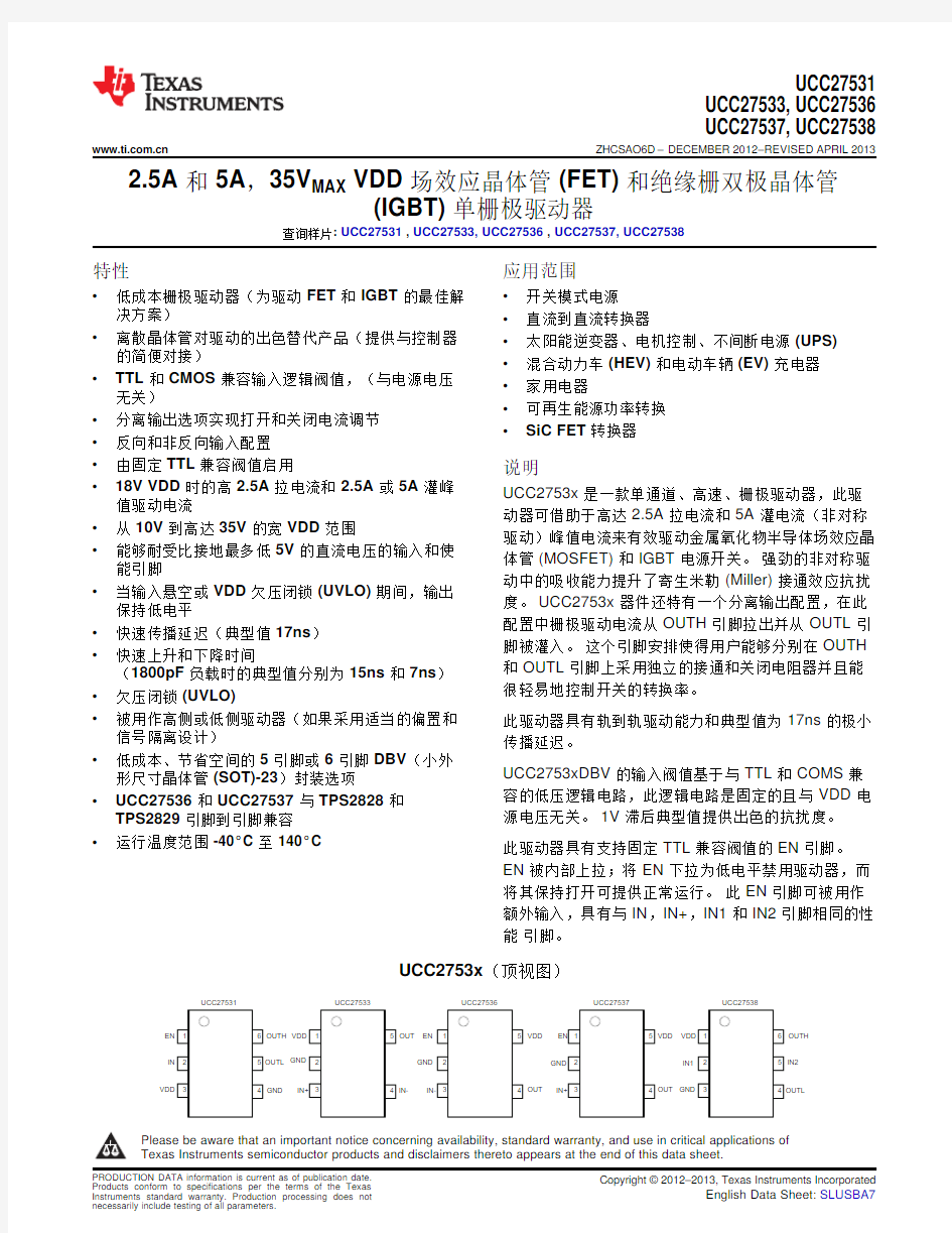
?低成本、节省空间的5引脚或6引脚DBV(小外
UCC2753xDBV的输入阀值基于与TTL和COMS兼形尺寸晶体管(SOT)-23)封装选项
容的低压逻辑电路,此逻辑电路是固定的且与VDD电?UCC27536和UCC27537与TPS2828和
源电压无关。1V滞后典型值提供出色的抗扰度。
TPS2829引脚到引脚兼容
?运行温度范围-40°C至140°C此驱动器具有支持固定TTL兼容阀值的EN引脚。
EN被内部上拉;将EN下拉为低电平禁用驱动器,而
将其保持打开可提供正常运行。此EN引脚可被用作
额外输入,具有与IN,IN+,IN1和IN2引脚相同的性
能引脚。
UCC2753x(顶视图)
Please be aware that an important notice concerning availability,standard warranty,and use in critical applications of
UCC27531
UCC27533,UCC27536
UCC27537,UCC27538
ZHCSAO6D–DECEMBER2012–REVISED https://www.doczj.com/doc/829132851.html, This integrated circuit can be damaged by ESD.Texas Instruments recommends that all integrated circuits be handled with appropriate precautions.Failure to observe proper handling and installation procedures can cause damage.
ESD damage can range from subtle performance degradation to complete device failure.Precision integrated circuits may be more susceptible to damage because very small parametric changes could cause the device not to meet its published specifications.
DESCRIPTION(CONT.)
Leaving the input pin of driver open holds the output low.The logic behavior of the driver is shown in the application diagram,timing diagram and input and output logic truth table.
Internal circuitry on VDD pin provides an under voltage lockout function that holds output low until VDD supply voltage is within operating range.
The UCC2753x driver is offered in a5-pin or6-pin standard SOT-23(DBV)package.The device operates over wide temperature range of-40°C to140°C.
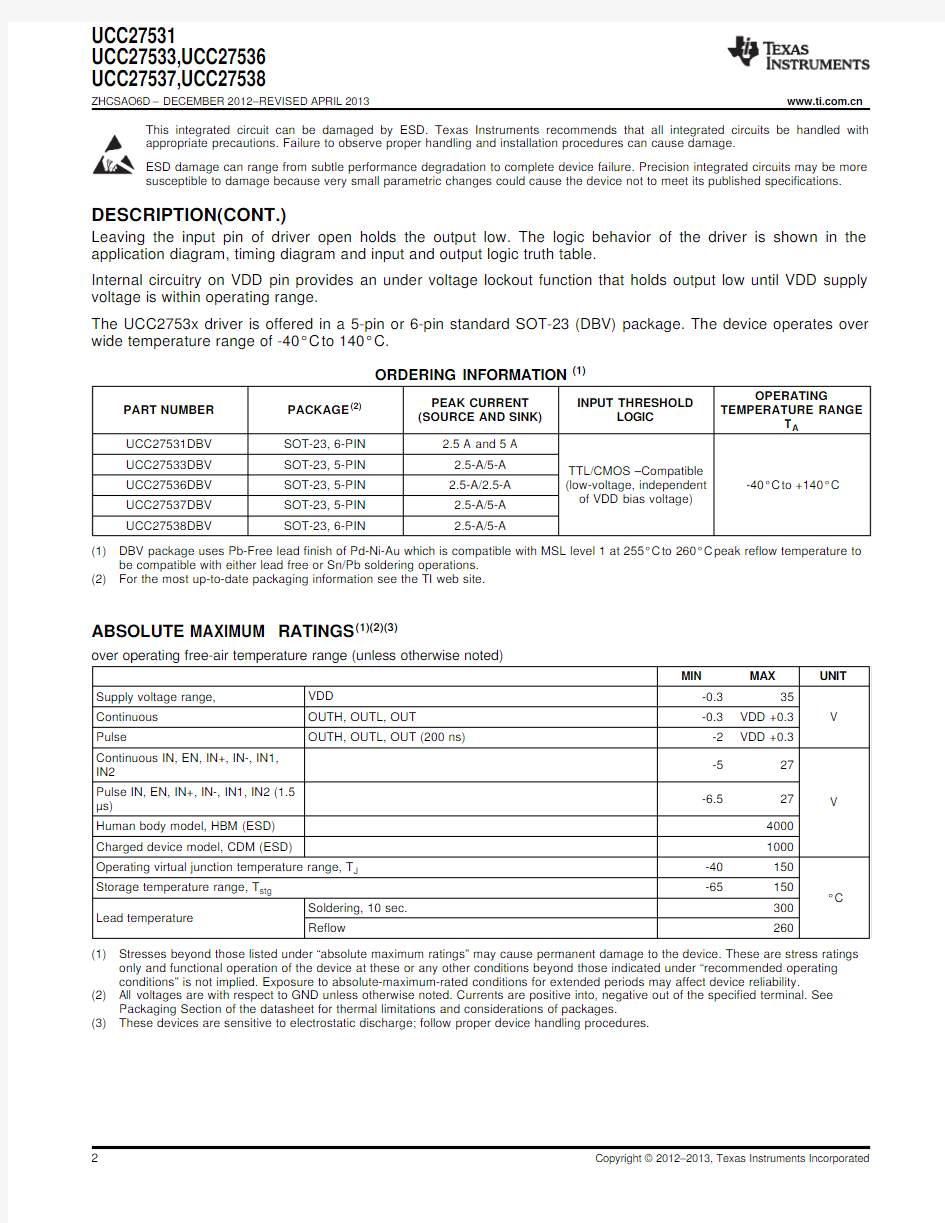
ORDERING INFORMATION(1)
OPERATING
PEAK CURRENT INPUT THRESHOLD
PART NUMBER PACKAGE(2)TEMPERATURE RANGE
(SOURCE AND SINK)LOGIC
T A UCC27531DBV SOT-23,6-PIN 2.5A and5A
UCC27533DBV SOT-23,5-PIN 2.5-A/5-A TTL/CMOS–Compatible
UCC27536DBV SOT-23,5-PIN 2.5-A/2.5-A(low-voltage,independent-40°C to+140°C
of VDD bias voltage)
UCC27537DBV SOT-23,5-PIN 2.5-A/5-A
UCC27538DBV SOT-23,6-PIN 2.5-A/5-A
(1)DBV package uses Pb-Free lead finish of Pd-Ni-Au which is compatible with MSL level1at255°C to260°C peak reflow temperature to
be compatible with either lead free or Sn/Pb soldering operations.
(2)For the most up-to-date packaging information see the TI web site.
ABSOLUTE MAXIMUM RATINGS(1)(2)(3)
over operating free-air temperature range(unless otherwise noted)
MIN MAX UNIT Supply voltage range,VDD-0.335
Continuous OUTH,OUTL,OUT-0.3VDD+0.3V Pulse OUTH,OUTL,OUT(200ns)-2VDD+0.3
Continuous IN,EN,IN+,IN-,IN1,
-527
IN2
Pulse IN,EN,IN+,IN-,IN1,IN2(1.5
-6.527V
μs)
Human body model,HBM(ESD)4000
Charged device model,CDM(ESD)1000
Operating virtual junction temperature range,T J-40150
Storage temperature range,T stg-65150
°C
Soldering,10sec.300
Lead temperature
Reflow260
(1)Stresses beyond those listed under“absolute maximum ratings”may cause permanent damage to the device.These are stress ratings
only and functional operation of the device at these or any other conditions beyond those indicated under“recommended operating conditions”is not implied.Exposure to absolute-maximum-rated conditions for extended periods may affect device reliability.
(2)All voltages are with respect to GND unless otherwise noted.Currents are positive into,negative out of the specified terminal.See
Packaging Section of the datasheet for thermal limitations and considerations of packages.
(3)These devices are sensitive to electrostatic discharge;follow proper device handling procedures.
UCC27531
UCC27533,UCC27536
UCC27537,UCC27538 https://www.doczj.com/doc/829132851.html, ZHCSAO6D–DECEMBER2012–REVISED APRIL2013 THERMAL INFORMATION
UCC27533,UCC27531,
UCC27536,UCC27538
UCC27537
THERMAL METRIC UNITS
DBV DBV(1)
5PINS6PINS
θJA Junction-to-ambient thermal resistance(2)178.3178.3
θJCtop Junction-to-case(top)thermal resistance(3)109.7109.7
θJB Junction-to-board thermal resistance(4)28.328.3°C/W
ψJT Junction-to-top characterization parameter(5)14.714.7
ψJB Junction-to-board characterization parameter(6)27.827.8
(1)For more information about traditional and new thermal metrics,see the IC Package Thermal Metrics application report,SPRA953.
(2)The junction-to-ambient thermal resistance under natural convection is obtained in a simulation on a JEDEC-standard,high-K board,as
specified in JESD51-7,in an environment described in JESD51-2a.
(3)The junction-to-case(top)thermal resistance is obtained by simulating a cold plate test on the package top.No specific JEDEC-
standard test exists,but a close description can be found in the ANSI SEMI standard G30-88.
(4)The junction-to-board thermal resistance is obtained by simulating in an environment with a ring cold plate fixture to control the PCB
temperature,as described in JESD51-8.
(5)The junction-to-top characterization parameter,ψJT,estimates the junction temperature of a device in a real system and is extracted
from the simulation data for obtainingθJA,using a procedure described in JESD51-2a(sections6and7).
(6)The junction-to-board characterization parameter,ψJB,estimates the junction temperature of a device in a real system and is extracted
from the simulation data for obtainingθJA,using a procedure described in JESD51-2a(sections6and7).
RECOMMENDED OPERATING CONDITIONS
over operating free-air temperature range(unless otherwise noted)
MIN TYP MAX UNIT Supply voltage range,VDD101832V Operating junction temperature range-40140°C
Input voltage,IN,IN+,IN-,IN1,IN2-525
V Enable,EN-525
UCC27531
UCC27533,UCC27536
UCC27537,UCC27538
ZHCSAO6D–DECEMBER2012–REVISED https://www.doczj.com/doc/829132851.html, ELECTRICAL CHARACTERISTICS
Unless otherwise noted,VDD=18V,T A=T J=-40°C to140°C,1-μF capacitor from VDD to GND,f=100kHz.Currents are positive into,negative out of the specified terminal.OUTH and OUTL are tied together for UCC27531/8.Typical condition specifications are at25°C.
PARAMETER TEST CONDITION MIN TYP MAX UNITS Bias Currents
VDD=7.0,IN,EN=VDD100200300
I DDoff Startup current(UCC25731)
IN,EN=GND100217300
VDD=7.0,IN+=GND,IN-=VDD100200300
I DDoff Startup current(UCC27533)
IN+=VDD,IN-=GND100217300
VDD=7.0,IN-=GND,EN=VDD100217300
I DDoff Startup current(UCC27536)μA
IN-=VDD,EN=GND100217300
VDD=7.0,IN+,EN=VDD100200300
I DDoff Startup current(UCC27537)
IN+,EN=GND100217300
VDD=7.0,IN1,IN2=VDD100200300
I DDoff Startup Current(UCC27538)
IN1,IN2=GND100200300
Under Voltage Lockout(UVLO)
V ON Supply start threshold8.08.99.8
Minimum operating voltage
V OFF7.38.29.1V after supply start
V DD_H Supply voltage hysteresis0.7
Input(IN,IN+,IN1,IN2)
Input signal high threshold,Output High,IN-=LOW,EN=HIGH,IN2or IN1=
V IN_H 1.8 2.0 2.2 output high HIGH(other is INPUT)
Input signal low threshold,Output Low,IN-=LOW,EN=HIGH,IN2or IN1=V
V IN_L0.8 1.0 1.2 output low HIGH(other is INPUT)
V IN_HYS Input signal hysteresis 1.0
Input(IN-)
Input signal high threshold,
V IN_H Output low,IN+=HIGH,EN=High 1.7 1.9 2.1 output low
Input signal low threshold,V
V IN_L Output high,,IN+=HIGH,EN=High0.8 1.0 1.2 output high
V IN_HYS Input signal hysteresis0.9
Enable(EN)
V EN_H Enable signal high threshold Output High 1.7 1.9 2.1
V EN_L Enable signal low threshold Output Low0.8 1.0 1.2V
V EN_HYS Enable signal hysteresis0.9
UCC27531
UCC27533,UCC27536
UCC27537,UCC27538 https://www.doczj.com/doc/829132851.html, ZHCSAO6D–DECEMBER2012–REVISED APRIL2013 ELECTRICAL CHARACTERISTICS(continued)
Unless otherwise noted,VDD=18V,T A=T J=-40°C to140°C,1-μF capacitor from VDD to GND,f=100kHz.Currents are positive into,negative out of the specified terminal.OUTH and OUTL are tied together for UCC27531/8.Typical condition specifications are at25°C.
PARAMETER TEST CONDITION MIN TYP MAX UNITS Outputs(OUTH/OUTL)
Source peak current(OUTH)/
I SRC/SNK CLOAD=0.22μF,f=1kHz-2.5/+5A
sink peak current(OUTL)(13)
VDD-VDD-
V OH OUTH,high voltage I OUTH=-10mA VDD-0.2
0.120.07
V OL OUTL,low voltage I OUTL=100mA0.0650.125V
OUTL,Low Voltage
V OL I OUTL=100mA0.1300.23 UCC27536
T A=25°C,I OUT=-10mA111212.5
R OH OUTH,pull-up resistance(15)
T A=-40°C to140°C,I OUT=-10mA71220
T A=25°C,I OUT=100mA0.450.650.85
R OL OUTL,pull-down resistance?
T A=-40°C to140°C,I OUT=100mA0.30.65 1.25
T A=25°C,I OUT=100mA0.9 1.3 1.7 OUTL,pull-down resistance
R OL
UCC27536T
=-40°C to140°C,I OUT=100mA0.6 1.3 2.3
A
Switching Time
t R Rise time C LOAD=1.8nF15
t F Fall time C LOAD=1.8nF7
t F Fall Time UCC27536DBV CLOAD=1.8nF10
t D1Turn-on propagation delay C LOAD=1.8nF,IN,IN+=0V to5V1726
ns
t D2Turn-off propagation delay C LOAD=1.8nF,IN,IN+=5V to0V1726
Inverting turn-off propagation
t D3C LOAD=1.8nF,IN-=0V to5V1728 delay
Inverting turn-on propagation
t D4C LOAD=1.8nF,IN-=5V to0V2028 delay
D2D2(IN-f r
D2D1IN-f
r UCC27531UCC27533,UCC27536UCC27537,UCC27538
ZHCSAO6D –DECEMBER 2012–REVISED APRIL https://www.doczj.com/doc/829132851.html,
Timing Diagram
Figure 1.UCC27531:(OUTPUT =OUTH tied to OUTL)INPUT =IN,(EN =VDD),or INPUT =EN,(IN =VDD)UCC27537:(OUTPUT =OUT)INPUT =IN+,(EN =VDD),or INPUT =EN,(IN+=VDD)UCC27538:(OUTPUT =OUTH tied to OUTL)INPUT =IN1,(IN2=VDD),or INPUT =IN2,(IN1=VDD)
Figure 2.UCC27533:(OUTPUT =OUT)INPUT =IN+UCC27536:(OUTPUT =OUT)INPUT =EN
Figure 3.UCC27533:(OUTPUT =OUT)ENABLE =IN+UCC27536:(OUTPUT =OUT)ENABLE =EN
VDD
OUT
EN IN-GND
VDD
OUT
IN+IN-
GND VDD
OUTH
OUTL
IN EN GND UCC27531UCC27533,UCC27536UCC27537,UCC27538
https://www.doczj.com/doc/829132851.html, ZHCSAO6D –DECEMBER 2012–REVISED APRIL 2013
DEVICE INFORMATION
Block Diagram
Figure 4.UCC27531(EN pull-up resistance to VREF =500k Ω,VREF =5.8V,in pull-down resistance to GND =230k Ω)
Figure 5.UCC27533(IN-pull-up resistance to VREF =500k Ω,VREF =5.8V,IN+pull-down resistance to GND =230k Ω)
Figure 6.UCC27536(EN pull-up resistance to VREF =500k Ω,VREF =5.8V,IN-pull-up resistance to VREF =500k Ω)
VDD
OUTH OUTL
IN1IN2GND
VDD
OUT
EN IN+GND UCC27531UCC27533,UCC27536UCC27537,UCC27538
ZHCSAO6D –DECEMBER 2012–REVISED APRIL https://www.doczj.com/doc/829132851.html,
Figure 7.UCC27537(EN pull-up resistance to VREF =500k Ω,VREF =5.8V,IN+pull-down resistance to GND =230k Ω)
Figure 8.UCC27538(IN1pull-down resistance to GND =230k Ω,IN2pull-down resistance to GND =230k Ω)
UCC27531UCC27533,UCC27536UCC27537,UCC27538
https://www.doczj.com/doc/829132851.html, ZHCSAO6D –DECEMBER 2012–REVISED APRIL 2013
DEVICE INFORMATION
Typical Application Diagrams
Figure 9.Driving IGBT Without Negative Bias
Figure 10.Driving IGBT With 13-V Negative Turn-Off Bias
UCC27531UCC27533,UCC27536UCC27537,UCC27538
ZHCSAO6D –DECEMBER 2012–REVISED APRIL https://www.doczj.com/doc/829132851.html,
Figure 11.Single Output Driver
Figure https://www.doczj.com/doc/829132851.html,ing UCC2753x Drivers in an Inverter
UCC27531
UCC27533,UCC27536
UCC27537,UCC27538 https://www.doczj.com/doc/829132851.html, ZHCSAO6D–DECEMBER2012–REVISED APRIL2013
DEVICE INFORMATION
UCC2753x Product Matrix
Table1.UCC2753x Product Matrix
UCC27531
UCC27533,UCC27536
UCC27537,UCC27538
ZHCSAO6D–DECEMBER2012–REVISED https://www.doczj.com/doc/829132851.html,
TERMINAL FUNCTIONS
TERMINAL
I/O FUNCTION
PIN NUMBER NAME
UCC27531DBV
Enable(Pull EN to GND in order to disable output,pull it high or leave open to enable 1EN I
output)
2IN I Driver non-inverting input
3VDD I Bias supply input
4GND-Ground(all signals are referenced to this node)
5OUTL O5-A sink current output of driver
6OUTH O 2.5-A Source Current Output of driver
UCC27533DBV
1VDD I Bias supply input
2GND-Ground(All signals are referenced to this node)
3IN+I Driver non-inverting input
4IN-I Driver inverting input
5OUT O 2.5-A source and5-A sink current output of driver
UCC27536DBV
Enable(pull EN to GND in order to disable output,pull it high or leave open to enable 1EN I
output)
2GND-Ground(all signals are referenced to this node)
3IN-I Driver inverting input
4OUT O 2.5-A source and2.5-A sink current output of driver
5VDD I Bias supply input
UCC27537DBV
Enable(Pull EN to GND in order to disable Output,Pull it high or leave open to 1EN I
enable Output)
2GND-Ground(All signals are referenced to this node)
3IN+I Driver non-inverting input
4OUT O 2.5-A source and5-A sink current output of driver
5VDD I Bias supply input
UCC27538DBV
1VDD I Bias supply input
2IN1I Driver non-inverting input
3GND-Ground(all signals are referenced to this node)
4OUTL O5-A sink current output of driver
5IN2I Driver non-inverting input
6OUTH O 2.5-A source current output of driver
UCC27531
UCC27533,UCC27536
UCC27537,UCC27538 https://www.doczj.com/doc/829132851.html, ZHCSAO6D–DECEMBER2012–REVISED APRIL2013
INPUT/OUTPUT LOGIC TRUTH TABLE
(for single output driver)
UCC27531DBV
OUT IN PIN EN PIN OUTH PIN OUTL PIN(OUTH and OUTL pins
tied together) L L High-impedance L L
L H High-impedance L L
H L High-impedance L L
H H H High-impedance H
H FLOAT H High-impedance H
FLOAT H High-impedance L L
INPUT/OUTPUT LOGIC TRUTH TABLE
UCC27533DBV
IN+PIN IN-PIN OUT PIN
L L L
L H L
H L H
H H L
FLOAT X L
X FLOAT L
UCC27536DBV
IN-PIN EN PIN OUT PIN
L L L
L H H
H L L
H H L
FLOAT X L
L FLOAT H
UCC27537DBV
IN+PIN EN PIN OUT PIN
L L L
L H L
H L L
H H H
FLOAT X L
H FLOAT H
INPUT/OUTPUT LOGIC TRUTH TABLE
(for single output driver)
UCC27538DBV
OUT IN1PIN IN2PIN OUTH PIN OUTL PIN(OUTH and OUTL pins
tied together) L L High-Impedance L L
L H High-Impedance L L
H L High-Impedance L L
H H H High-Impedance H
X FLOAT High-Impedance L L FLOAT X High-Impedance L L
UCC27531
UCC27533,UCC27536
UCC27537,UCC27538
ZHCSAO6D–DECEMBER2012–REVISED https://www.doczj.com/doc/829132851.html,
TYPICAL CHARACTERISTICS
If not specified,INPUT refers to non-inverting input
Figure16.Propagation Delay vs.Supply Voltage
UCC27531UCC27533,UCC27536UCC27537,UCC27538
https://www.doczj.com/doc/829132851.html, ZHCSAO6D –DECEMBER 2012–REVISED APRIL 2013
TYPICAL CHARACTERISTICS (continued)
If not specified,INPUT refers to non-inverting input
Figure 19.UCC27533Start-Up Current vs.Temperature
UCC27531UCC27533,UCC27536UCC27537,UCC27538
ZHCSAO6D –DECEMBER 2012–REVISED APRIL https://www.doczj.com/doc/829132851.html,
TYPICAL CHARACTERISTICS (continued)
If not specified,INPUT refers to non-inverting input
Figure 23.UCC27537Start-Up Current vs.Temperature (output switching)
UCC27531UCC27533,UCC27536UCC27537,UCC27538
https://www.doczj.com/doc/829132851.html, ZHCSAO6D –DECEMBER 2012–REVISED APRIL 2013
TYPICAL CHARACTERISTICS (continued)
If not specified,INPUT refers to non-inverting input
Figure 27.IN-Input Threshold vs.Temperature
UCC27531UCC27533,UCC27536UCC27537,UCC27538
ZHCSAO6D –DECEMBER 2012–REVISED APRIL https://www.doczj.com/doc/829132851.html,
TYPICAL CHARACTERISTICS (continued)
If not specified,INPUT refers to non-inverting input
(output in DC on/off condition)Temperature
UCC27531UCC27533,UCC27536UCC27537,UCC27538
https://www.doczj.com/doc/829132851.html, ZHCSAO6D –DECEMBER 2012–REVISED APRIL 2013
TYPICAL CHARACTERISTICS (continued)
If not specified,INPUT refers to non-inverting input
Figure 33.IN-Input-to-Output Propagation Delay vs.Temperature
Figure 36.UCC27536Fall Time vs.Temperature
UCC27531UCC27533,UCC27536UCC27537,UCC27538
ZHCSAO6D –DECEMBER 2012–REVISED APRIL https://www.doczj.com/doc/829132851.html,
TYPICAL CHARACTERISTICS (continued)
If not specified,INPUT refers to non-inverting input
(output switching)
Figure 40.UCC27536Fall Time vs.Supply Voltage