https://www.doczj.com/doc/896815290.html, FEATURES
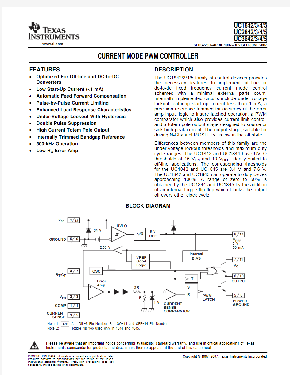
DESCRIPTION BLOCK DIAGRAM
A/B V cc R T /C T V CURRENT SENSE Note 1:Note 2: A = DIL?8 Pin Number. B = SO?14 and CFP?14 Pin Number.
T oggle flip flop used only in 1844 and 1845.UC1842/3/4/5UC2842/3/4/5UC3842/3/4/5SLUS223C–APRIL 1997–REVISED JUNE 2007
CURRENT MODE PWM CONTROLLER
?
Optimized For Off-line and DC-to-DC The UC1842/3/4/5family of control devices provides Converters the necessary features to implement off-line or dc-to-dc fixed frequency current mode control ?
Low Start-Up Current (<1mA)schemes with a minimal external parts count.?
Automatic Feed Forward Compensation Internally implemented circuits include under-voltage ?
Pulse-by-Pulse Current Limiting lockout featuring start up current less than 1mA,a precision reference trimmed for accuracy at the error ?
Enhanced Load Response Characteristics amp input,logic to insure latched operation,a PWM ?
Under-Voltage Lockout With Hysteresis comparator which also provides current limit control,?
Double Pulse Suppression and a totem pole output stage designed to source or sink high peak current.The output stage,suitable for ?
High Current Totem Pole Output driving N-Channel MOSFETs,is low in the off state.?
Internally Trimmed Bandgap Reference Differences between members of this family are the ?
500-kHz Operation under-voltage lockout thresholds and maximum duty
?Low R O Error Amp cycle ranges.The UC1842and UC1844have UVLO
thresholds of 16V ON and 10V OFF ,ideally suited to
off-line applications.The corresponding thresholds
for the UC1843and UC1845are 8.4V and 7.6V.
The UC1842and UC1843can operate to duty cycles
approaching 100%.A range of zero to 50%is
obtained by the UC1844and UC1845by the addition
of an internal toggle flip flop which blanks the output
off every other clock cycle.
Please be aware that an important notice concerning availability,standard warranty,and use in critical applications of Texas
Instruments semiconductor products and disclaimers thereto appears at the end of this data sheet.
https://www.doczj.com/doc/896815290.html, ABSOLUTE MAXIMUM RATINGS (1)
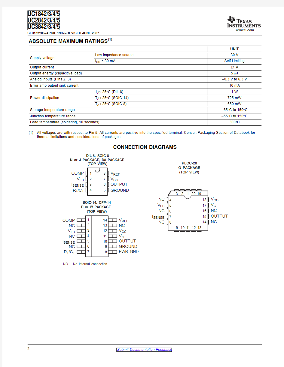
CONNECTION DIAGRAMS 12348765COMP
V FB
I SENSE
R T /C T V REF V CC OUTPUT GROUND
DIL-8, SOIC-8
N or J PACKAGE, D8 PACKAGE
(TOP VIEW)NC ? No internal connection 1234 567141312111098
COMP NC V FB NC I SENSE NC R T /C T SOIC-14, CFP-14D or W PACKAGE (TOP VIEW)V REF
NC
V CC
V C
OUTPUT
GROUND
PWR GND 3212019910111213456781817161514V CC V C NC OUTPUT NC NC
V FB
NC
I SENSE NC PLCC-20
Q PACKAGE
(TOP VIEW)N C C O M P N C P W R G N D G R O U N D
N C N C N C R T /C T V R E F UC1842/3/4/5UC2842/3/4/5UC3842/3/4/5
SLUS223C–APRIL 1997–REVISED JUNE 2007UNIT
Low impedance source 30V Supply voltage
I CC <30mA Self Limiting Output current
±1A Output energy (capacitive load)
5μJ Analog inputs (Pins 2,3)
–0.3V to 6.3V Error amp output sink current
10mA T A ≤25°C (DIL-8)
1W Power dissipation
T A ≤25°C (SOIC-14)725mW T A ≤25°C (SOIC-8)650mW Storage temperature range
–65°C to 150°C Junction temperature range
–55°C to 150°C Lead temperature (soldering,10seconds)
300°C (1)All voltages are with respect to Pin 5.All currents are positive into the specified terminal.Consult Packaging Section of Databook for thermal limitations and considerations of packages.
https://www.doczj.com/doc/896815290.html,
Temp Stability+V REF(max)*VREF(min)
TJ(max)*TJ(min)V
REF(max)
and V REF(min)are the maximum and minimum reference voltages measured over
THERMAL CHARACTERISTICS
DISSIPATION RATINGS ELECTRICAL CHARACTERISTICS
UC1842/3/4/5
UC2842/3/4/5
UC3842/3/4/5 SLUS223C–APRIL1997–REVISED JUNE2007
over operating free-air temperature range(unless otherwise noted)
PACKAGEθJCθJA
DIL-8J28(1)125-160
N25110(2)
SOIC-8D84284-160(2)
SOIC-14D143550-120(2)
CFP-14W 5.49°C/W175.4C/W
PLCC-20Q3443-75(2)
(1)θJC data values stated were derived from MIL-STD-1835B.
(2)SpecifiedθJA(junction to ambient)is for devices mounted to5in2FR4PC board with one ounce copper where noted.When resistance
range is given,lower values are for5in2.Test PWB was0.062in thick and typically used0.635-mm trace widths for power packages and1.3-mm trace widths for non-power packages with100x100-mil probe land area at the end of each trace.
T A≤25°C DERATING FACTOR T A≤70°C T A≤85°CPO T A≤125°C PACKAGE
POWER RATING ABOVE T A≤25°C POWER RATING WER RATING POWER RATING W700mW 5.5mW/°C452mW370mW150mW
Unless otherwise stated,these specifications apply for–55°C≤T
A ≤125°C for the UC184X;–40°C≤T A≤85°C for the
UC284X;0°C≤T
A
≤70°C for the384X;V CC=15V(1);R T=10k?;C T=3.3nF,T A=T J.
UC1842/3/4/5
UC3842/3/4/5
UC2842/3/4/5
PARAMETER TEST CONDITIONS UNIT
MIN TYP MAX MIN TYP MAX REFERENCE SECTION
Output Voltage T J=25°C,I O=1mA 4.95 5.00 5.05 4.90 5.00 5.10V Line Regulation12≤V IN≤25V620620
mV Load Regulation1≤I0≤20mA625625
Temp.Stability See(2)(3)0.20.40.20.4mV/°C Total Output Variation Line,load,tempature(2) 4.9 5.1 4.82 5.18V Output Noise Voltage10Hz≤f≤10kHz,T J=25°C(2)5050μV Long Term Stability T A=125°C,1000Hrs(2)525525mV Output Short Circuit–30–100–180–30–100–180mA OSCILLATOR SECTION
Initial Accuracy T J=25°C(4)475257475257kHz Voltage Stability12≤V CC≤25V0.2%1%0.2%1% Temp.Stability T MIN≤T A≤T MAX(2)5%5%
Amplitude V PIN4peak-to-peak(2) 1.7 1.7V
(1)Adjust V CC above the start threshold before setting at15V.
(2)These parameters,although specified,are not100%tested in production.
(3)Temperature stability,sometimes referred to as average temperature coefficient,is described by the equation:
the appropriate temperature range.Note that the extremes in voltage do not necessarily occur at the extremes in temperature.
(4)Output frequency equals oscillator frequency for the UC1842and UC1843.
Output frequency is one half oscillator frequency for the UC1844and UC1845.
https://www.doczj.com/doc/896815290.html,
(7)Gain defined as:A+D VPIN1
D VPIN3
,0v VPIN3v0.8V
UC1842/3/4/5
UC2842/3/4/5
UC3842/3/4/5
SLUS223C–APRIL1997–REVISED JUNE2007
ELECTRICAL CHARACTERISTICS(continued)
Unless otherwise stated,these specifications apply for–55°C≤T A≤125°C for the UC184X;–40°C≤T A≤85°C for the
UC284X;0°C≤T A≤70°C for the384X;V CC=15V;R T=10k?;C T=3.3nF,T A=T J.
UC1842/3/4/5
UC3842/3/4/5
UC2842/3/4/5
PARAMETER TEST CONDITIONS UNIT
MIN TYP MAX MIN TYP MAX
ERROR AMP SECTION
Input Voltage V PIN1=2.5V 2.45 2.50 2.55 2.42 2.50 2.58V
Input Bias Current–0.3–1–0.3–2μA
A VOL2≤V O≤4V65906590d
B Unity Gain Bandwidth T J=25°C(5)0.710.71MHz
PSRR12≤V CC≤25V60706070dB Output Sink Current V PIN2=2.7V,V PIN1=1.1V2626
mA Output Source Current V PIN2=2.3V,V PIN1=5V–0.5–0.8–0.5–0.8
V OUT High V PIN2=2.3V,R L=15k?to ground5656
V V OUT Low V PIN2=2.7V,R L=15k?to Pin80.7 1.10.7 1.1 CURRENT SENSE SECTION
Gain See(6)(7) 2.853 3.15 2.853 3.15V/V
Maximum Input Signal V PIN1=5V(6)0.91 1.10.91 1.1V
PSRR12≤V CC≤25V(5)(6)7070dB Input Bias Current–2–10–2–10μA Delay to Output V PIN3=0V to2V(5)150300150300ns OUTPUT SECTION
I SINK=20mA0.10.40.10.4
Output Low Level
I SINK=200mA 1.5 2.2 1.5 2.2
V
I SOURCE=20mA1313.51313.5
Output High Level
I SOURCE=200mA1213.51213.5
Rise Time T J=25°C,C L=1nF(5)5015050150
ns Fall Time T J=25°C,C L=1nF(5)5015050150
UNDER-VOLTAGE LOCKOUT SECTION
X842/415161714.51617.5
Start Threshold
X843/57.88.49.07.88.49.0
V
X842/4910118.51011.5
Min.Operating Voltage After
Turn On X843/57.07.68.27.07.68.2
PWM SECTION
X842/395%97%100%95%97%100% Maximum Duty Cycle
X844/546%48%50%47%48%50%
Minimum Duty Cycle0%0%
TOTAL STANDBY CURRENT
Start-Up Current0.510.51
mA Operating Supply Current V PIN2=V PIN3=0V11171117
V CC Zener Voltager I CC=25mA30343034V
(5)These parameters,although specified,are not100%tested in production.
(6)Parameter measured at trip point of latch with V PIN2=0.
https://www.doczj.com/doc/896815290.html, ERROR AMP CONFIGURATION
UNDER-VOLTAGE LOCKOUT
<17 mA <1 mA
V OFF V ON V CC
V CC CURRENT SENSE CIRCUIT
Peak Current (I S
) is Determined By The Formula
,1.0 V RS I SMAX UC1842/3/4/5UC2842/3/4/5UC3842/3/4/5SLUS223C–APRIL 1997–REVISED JUNE 2007Error amp can source or sink up to 0.5mA.
During under-voltage lock-out,the output drive is biased to sink minor amounts of current.Pin 6should be shunted to ground with a bleeder resistor to prevent activating the power switch with extraneous leakage currents.
A small RC filter may be required to suppress switch transients.
https://www.doczj.com/doc/896815290.html, OSCILLATOR
SECTION
V REF R T /C T GROUND R T C T
For R T > 5 K f ~ 1.72R T C T 30103
1
0.3
t d ? m s 1
2.2 4.7102247100C T ? nF Deadtime vs C T (R T >5 k W )R T ? (k )W 3 f ? Frequency ? Hz
Timing Resistance vs Frequency OUTPUT SATURATION CHARACTERISTICS
4
3
2
10
Output Current, Source or Sink ? A
S a t u r a t i o n V o l t a g e ? V ERROR AMPLIFIER OPEN-LOOP FREQUENCY RESPONSE
80604020
00
?45
?90
?135?180
V o l t a g e G a i n ? d B P h a s e M a r g i n ? °f ? Frequency ? Hz
UC1842/3/4/5UC2842/3/4/5UC3842/3/4/5
SLUS223C–APRIL 1997–REVISED JUNE 2007
https://www.doczj.com/doc/896815290.html, OPEN-LOOP LABORATORY FIXTURE
4.7 k W
1 k W ERROR AMP ADJUST
4.7 k W
V REF
V CC OUTPUT GROUND
SHUTDOWN
TECHNIQUES
SHUTDOWN SHUTDOWN UC1842/3/4/5UC2842/3/4/5UC3842/3/4/5SLUS223C–APRIL 1997–REVISED JUNE 2007High peak currents associated with capacitive loads necessitate careful grounding techniques.Timing and bypas capacitors should be conected close to pin 5in a single point ground.The transistor and 5k potentiometer are used to sample the oscillator waveform and apply an adjustable ramp to pin 3.
Shutdown of the UC1842can be accomplished by two methods;either raise pin 3above 1V or pull pin 1below a voltage two diode drops above ground.Either method causses the output of the PWM comparator to be high (refer to block diagram).The PWM latch is reset dominant so that the output will remain low until the next clock cycle after the shutdown condition at pin 1and/or 3is removed.In one example,an externally latched shutdown may be accomplished by adding an SCR which will be reset by cycling V CC below the lower UVLO threshold.At this pint the reference turns off,allowing the SCR to reset.
https://www.doczj.com/doc/896815290.html, OFFLINE FLYBACK REGULATOR
R1
T1D6L1+6 V COM +12 V
±12 V COM ?12 V
Power Supply Specifications
SLOPE COMPENSATION
UC1842/3/4/5UC2842/3/4/5UC3842/3/4/5
SLUS223C–APRIL 1997–REVISED JUNE 20071.Input Voltages
a.5VAC to 130VA (50Hz/60Hz)
2.Line Isolation:3750V
3.Switchng Frequency:40kHz
4.Efficiency at Full Load 70%
5.Output Voltage:
a.+5V,±5%;1A to 4A load
Ripple voltage:50mV P-P Max
b.+12V,±3%;0.1A to 0.3A load
Ripple voltage:100mV P-P Max
c.–12V,±3%;0.1A to 0.3A load
Ripple voltage:100mV P-P Max
A fraction of the oscillator ramp can be resistively summed with the current sense signal to provide slope compensation for converters requiring duty cycles over 50%.
PACKAGING INFORMATION
Orderable Device Status(1)Package
Type Package
Drawing
Pins Package
Qty
Eco Plan(2)Lead/Ball Finish MSL Peak Temp(3)
5962-8670401PA ACTIVE CDIP JG81TBD A42N/A for Pkg Type 5962-8670401XA ACTIVE LCCC FK201TBD POST-PLATE N/A for Pkg Type 5962-8670402PA ACTIVE CDIP JG81TBD A42N/A for Pkg Type 5962-8670402XA ACTIVE LCCC FK201TBD POST-PLATE N/A for Pkg Type 5962-8670403PA ACTIVE CDIP JG81TBD A42N/A for Pkg Type 5962-8670403XA ACTIVE LCCC FK201TBD POST-PLATE N/A for Pkg Type 5962-8670404DA ACTIVE CFP W141TBD A42N/A for Pkg Type 5962-8670404PA ACTIVE CDIP JG81TBD A42N/A for Pkg Type 5962-8670404XA ACTIVE LCCC FK201TBD POST-PLATE N/A for Pkg Type UC1842J ACTIVE CDIP JG81TBD A42N/A for Pkg Type UC1842J883B ACTIVE CDIP JG81TBD A42N/A for Pkg Type UC1842L883B ACTIVE LCCC FK201TBD POST-PLATE N/A for Pkg Type UC1842W ACTIVE CFP W141TBD A42N/A for Pkg Type UC1843J ACTIVE CDIP JG81TBD A42N/A for Pkg Type UC1843J883B ACTIVE CDIP JG81TBD A42N/A for Pkg Type UC1843L ACTIVE LCCC FK201TBD POST-PLATE N/A for Pkg Type UC1843L883B ACTIVE LCCC FK201TBD POST-PLATE N/A for Pkg Type UC1843W ACTIVE CFP W141TBD A42N/A for Pkg Type UC1844J ACTIVE CDIP JG81TBD A42N/A for Pkg Type UC1844J883B ACTIVE CDIP JG81TBD A42N/A for Pkg Type UC1844L883B ACTIVE LCCC FK201TBD POST-PLATE N/A for Pkg Type UC1845J ACTIVE CDIP JG81TBD A42N/A for Pkg Type UC1845J883B ACTIVE CDIP JG81TBD A42N/A for Pkg Type UC1845L ACTIVE LCCC FK201TBD POST-PLATE N/A for Pkg Type UC1845L883B ACTIVE LCCC FK201TBD POST-PLATE N/A for Pkg Type UC1845W ACTIVE CFP W141TBD A42N/A for Pkg Type UC1845W883B ACTIVE CFP W141TBD A42N/A for Pkg Type UC2842D ACTIVE SOIC D1450Green(RoHS&
no Sb/Br)
CU NIPDAU Level-1-260C-UNLIM
UC2842D8ACTIVE SOIC D875Green(RoHS&
no Sb/Br)
CU NIPDAU Level-1-260C-UNLIM
UC2842D8G4ACTIVE SOIC D875Green(RoHS&
no Sb/Br)
CU NIPDAU Level-1-260C-UNLIM
UC2842D8TR ACTIVE SOIC D82500Green(RoHS&
no Sb/Br)
CU NIPDAU Level-1-260C-UNLIM
UC2842D8TRG4ACTIVE SOIC D82500Green(RoHS&
no Sb/Br)
CU NIPDAU Level-1-260C-UNLIM
UC2842DG4ACTIVE SOIC D1450Green(RoHS&
no Sb/Br)
CU NIPDAU Level-1-260C-UNLIM
UC2842DTR ACTIVE SOIC D142500Green(RoHS&
no Sb/Br)
CU NIPDAU Level-1-260C-UNLIM
UC2842DTRG4ACTIVE SOIC D142500Green(RoHS&
no Sb/Br)
CU NIPDAU Level-1-260C-UNLIM UC2842J OBSOLETE CDIP JG8TBD Call TI Call TI
Orderable Device Status(1)Package
Type Package
Drawing
Pins Package
Qty
Eco Plan(2)Lead/Ball Finish MSL Peak Temp(3)
UC2842N ACTIVE PDIP P850Green(RoHS&
no Sb/Br)
CU NIPDAU N/A for Pkg Type
UC2842NG4ACTIVE PDIP P850Green(RoHS&
no Sb/Br)
CU NIPDAU N/A for Pkg Type UC2842P OBSOLETE PDIP P8TBD Call TI Call TI
UC2843D ACTIVE SOIC D1450Green(RoHS&
no Sb/Br)
CU NIPDAU Level-1-260C-UNLIM
UC2843D8ACTIVE SOIC D875Green(RoHS&
no Sb/Br)
CU NIPDAU Level-1-260C-UNLIM
UC2843D8G4ACTIVE SOIC D875Green(RoHS&
no Sb/Br)
CU NIPDAU Level-1-260C-UNLIM
UC2843D8TR ACTIVE SOIC D82500Green(RoHS&
no Sb/Br)
CU NIPDAU Level-1-260C-UNLIM
UC2843D8TRG4ACTIVE SOIC D82500Green(RoHS&
no Sb/Br)
CU NIPDAU Level-1-260C-UNLIM
UC2843DG4ACTIVE SOIC D1450Green(RoHS&
no Sb/Br)
CU NIPDAU Level-1-260C-UNLIM
UC2843DTR ACTIVE SOIC D142500Green(RoHS&
no Sb/Br)
CU NIPDAU Level-1-260C-UNLIM
UC2843DTRG4ACTIVE SOIC D142500Green(RoHS&
no Sb/Br)
CU NIPDAU Level-1-260C-UNLIM UC2843J OBSOLETE CDIP JG8TBD Call TI Call TI
UC2843N ACTIVE PDIP P850Green(RoHS&
no Sb/Br)
CU NIPDAU N/A for Pkg Type
UC2843NG4ACTIVE PDIP P850Green(RoHS&
no Sb/Br)
CU NIPDAU N/A for Pkg Type
UC2844D ACTIVE SOIC D1450Green(RoHS&
no Sb/Br)
CU NIPDAU Level-1-260C-UNLIM
UC2844D8ACTIVE SOIC D875Green(RoHS&
no Sb/Br)
CU NIPDAU Level-1-260C-UNLIM
UC2844D8G4ACTIVE SOIC D875Green(RoHS&
no Sb/Br)
CU NIPDAU Level-1-260C-UNLIM
UC2844D8TR ACTIVE SOIC D82500Green(RoHS&
no Sb/Br)
CU NIPDAU Level-1-260C-UNLIM
UC2844D8TRG4ACTIVE SOIC D82500Green(RoHS&
no Sb/Br)
CU NIPDAU Level-1-260C-UNLIM
UC2844DG4ACTIVE SOIC D1450Green(RoHS&
no Sb/Br)
CU NIPDAU Level-1-260C-UNLIM
UC2844DTR ACTIVE SOIC D142500Green(RoHS&
no Sb/Br)
CU NIPDAU Level-1-260C-UNLIM
UC2844DTRG4ACTIVE SOIC D142500Green(RoHS&
no Sb/Br)
CU NIPDAU Level-1-260C-UNLIM
UC2844N ACTIVE PDIP P850Green(RoHS&
no Sb/Br)
CU NIPDAU N/A for Pkg Type
UC2844NG4ACTIVE PDIP P850Green(RoHS&
no Sb/Br)
CU NIPDAU N/A for Pkg Type
UC2845D ACTIVE SOIC D1450Green(RoHS&
no Sb/Br)
CU NIPDAU Level-1-260C-UNLIM
UC2845D8ACTIVE SOIC D875Green(RoHS&
no Sb/Br)
CU NIPDAU Level-1-260C-UNLIM
UC2845D8G4ACTIVE SOIC D875Green(RoHS&CU NIPDAU Level-1-260C-UNLIM
Orderable Device Status(1)Package
Type Package
Drawing
Pins Package
Qty
Eco Plan(2)Lead/Ball Finish MSL Peak Temp(3)
no Sb/Br)
UC2845D8TR ACTIVE SOIC D82500Green(RoHS&
no Sb/Br)
CU NIPDAU Level-1-260C-UNLIM
UC2845D8TRG4ACTIVE SOIC D82500Green(RoHS&
no Sb/Br)
CU NIPDAU Level-1-260C-UNLIM
UC2845DG4ACTIVE SOIC D1450Green(RoHS&
no Sb/Br)
CU NIPDAU Level-1-260C-UNLIM
UC2845DTR ACTIVE SOIC D142500Green(RoHS&
no Sb/Br)
CU NIPDAU Level-1-260C-UNLIM
UC2845DTRG4ACTIVE SOIC D142500Green(RoHS&
no Sb/Br)
CU NIPDAU Level-1-260C-UNLIM UC2845J OBSOLETE CDIP JG8TBD Call TI Call TI
UC2845N ACTIVE PDIP P850Green(RoHS&
no Sb/Br)
CU NIPDAU N/A for Pkg Type
UC2845NG4ACTIVE PDIP P850Green(RoHS&
no Sb/Br)
CU NIPDAU N/A for Pkg Type
UC3842D ACTIVE SOIC D1450Green(RoHS&
no Sb/Br)
CU NIPDAU Level-1-260C-UNLIM
UC3842D8ACTIVE SOIC D875Green(RoHS&
no Sb/Br)
CU NIPDAU Level-1-260C-UNLIM
UC3842D8G4ACTIVE SOIC D875Green(RoHS&
no Sb/Br)
CU NIPDAU Level-1-260C-UNLIM
UC3842D8TR ACTIVE SOIC D82500Green(RoHS&
no Sb/Br)
CU NIPDAU Level-1-260C-UNLIM
UC3842D8TRG4ACTIVE SOIC D82500Green(RoHS&
no Sb/Br)
CU NIPDAU Level-1-260C-UNLIM
UC3842DG4ACTIVE SOIC D1450Green(RoHS&
no Sb/Br)
CU NIPDAU Level-1-260C-UNLIM
UC3842DTR ACTIVE SOIC D142500Green(RoHS&
no Sb/Br)
CU NIPDAU Level-1-260C-UNLIM
UC3842DTRG4ACTIVE SOIC D142500Green(RoHS&
no Sb/Br)
CU NIPDAU Level-1-260C-UNLIM
UC3842N ACTIVE PDIP P850Green(RoHS&
no Sb/Br)
CU NIPDAU N/A for Pkg Type
UC3842NG4ACTIVE PDIP P850Green(RoHS&
no Sb/Br)
CU NIPDAU N/A for Pkg Type UC3842P OBSOLETE PDIP P8TBD Call TI Call TI
UC3843D ACTIVE SOIC D1450Green(RoHS&
no Sb/Br)
CU NIPDAU Level-1-260C-UNLIM
UC3843D8ACTIVE SOIC D875Green(RoHS&
no Sb/Br)
CU NIPDAU Level-1-260C-UNLIM
UC3843D8G4ACTIVE SOIC D875Green(RoHS&
no Sb/Br)
CU NIPDAU Level-1-260C-UNLIM
UC3843D8TR ACTIVE SOIC D82500Green(RoHS&
no Sb/Br)
CU NIPDAU Level-1-260C-UNLIM
UC3843D8TRG4ACTIVE SOIC D82500Green(RoHS&
no Sb/Br)
CU NIPDAU Level-1-260C-UNLIM
UC3843DG4ACTIVE SOIC D1450Green(RoHS&
no Sb/Br)
CU NIPDAU Level-1-260C-UNLIM
UC3843DTR ACTIVE SOIC D142500Green(RoHS&
no Sb/Br)
CU NIPDAU Level-1-260C-UNLIM
Orderable Device Status(1)Package
Type Package
Drawing
Pins Package
Qty
Eco Plan(2)Lead/Ball Finish MSL Peak Temp(3)
UC3843DTRG4ACTIVE SOIC D142500Green(RoHS&
no Sb/Br)
CU NIPDAU Level-1-260C-UNLIM
UC3843N ACTIVE PDIP P850Green(RoHS&
no Sb/Br)
CU NIPDAU N/A for Pkg Type
UC3843NG4ACTIVE PDIP P850Green(RoHS&
no Sb/Br)
CU NIPDAU N/A for Pkg Type UC3843P OBSOLETE PDIP P8TBD Call TI Call TI
UC3843QTR OBSOLETE PLCC FN20TBD Call TI Call TI
UC3844D ACTIVE SOIC D1450Green(RoHS&
no Sb/Br)
CU NIPDAU Level-1-260C-UNLIM
UC3844D8ACTIVE SOIC D875Green(RoHS&
no Sb/Br)
CU NIPDAU Level-1-260C-UNLIM
UC3844D8G4ACTIVE SOIC D875Green(RoHS&
no Sb/Br)
CU NIPDAU Level-1-260C-UNLIM
UC3844D8TR ACTIVE SOIC D82500Green(RoHS&
no Sb/Br)
CU NIPDAU Level-1-260C-UNLIM
UC3844D8TRG4ACTIVE SOIC D82500Green(RoHS&
no Sb/Br)
CU NIPDAU Level-1-260C-UNLIM
UC3844DG4ACTIVE SOIC D1450Green(RoHS&
no Sb/Br)
CU NIPDAU Level-1-260C-UNLIM
UC3844DTR ACTIVE SOIC D142500Green(RoHS&
no Sb/Br)
CU NIPDAU Level-1-260C-UNLIM
UC3844DTRG4ACTIVE SOIC D142500Green(RoHS&
no Sb/Br)
CU NIPDAU Level-1-260C-UNLIM
UC3844N ACTIVE PDIP P850Green(RoHS&
no Sb/Br)
CU NIPDAU N/A for Pkg Type
UC3844NG4ACTIVE PDIP P850Green(RoHS&
no Sb/Br)
CU NIPDAU N/A for Pkg Type UC3844P OBSOLETE PDIP P8TBD Call TI Call TI
UC3845AJ ACTIVE CDIP JG81TBD A42N/A for Pkg Type UC3845D ACTIVE SOIC D1450Green(RoHS&
no Sb/Br)
CU NIPDAU Level-1-260C-UNLIM
UC3845D8ACTIVE SOIC D875Green(RoHS&
no Sb/Br)
CU NIPDAU Level-1-260C-UNLIM
UC3845D8G4ACTIVE SOIC D875Green(RoHS&
no Sb/Br)
CU NIPDAU Level-1-260C-UNLIM
UC3845D8TR ACTIVE SOIC D82500Green(RoHS&
no Sb/Br)
CU NIPDAU Level-1-260C-UNLIM
UC3845D8TRG4ACTIVE SOIC D82500Green(RoHS&
no Sb/Br)
CU NIPDAU Level-1-260C-UNLIM
UC3845DG4ACTIVE SOIC D1450Green(RoHS&
no Sb/Br)
CU NIPDAU Level-1-260C-UNLIM
UC3845DTR ACTIVE SOIC D142500Green(RoHS&
no Sb/Br)
CU NIPDAU Level-1-260C-UNLIM
UC3845DTRG4ACTIVE SOIC D142500Green(RoHS&
no Sb/Br)
CU NIPDAU Level-1-260C-UNLIM
UC3845N ACTIVE PDIP P850Green(RoHS&
no Sb/Br)
CU NIPDAU N/A for Pkg Type
UC3845NG4ACTIVE PDIP P850Green(RoHS&
no Sb/Br)
CU NIPDAU N/A for Pkg Type
UC3845P OBSOLETE PDIP P8TBD Call TI Call TI
(1)The marketing status values are defined as follows:
ACTIVE:Product device recommended for new designs.
LIFEBUY:TI has announced that the device will be discontinued,and a lifetime-buy period is in effect.
NRND:Not recommended for new designs.Device is in production to support existing customers,but TI does not recommend using this part in a new design.
PREVIEW:Device has been announced but is not in production.Samples may or may not be available.
OBSOLETE:TI has discontinued the production of the device.
(2)Eco Plan-The planned eco-friendly classification:Pb-Free(RoHS),Pb-Free(RoHS Exempt),or Green(RoHS&no Sb/Br)-please check https://www.doczj.com/doc/896815290.html,/productcontent for the latest availability information and additional product content details.
TBD:The Pb-Free/Green conversion plan has not been defined.
Pb-Free(RoHS):TI's terms"Lead-Free"or"Pb-Free"mean semiconductor products that are compatible with the current RoHS requirements for all6substances,including the requirement that lead not exceed0.1%by weight in homogeneous materials.Where designed to be soldered at high temperatures,TI Pb-Free products are suitable for use in specified lead-free processes.
Pb-Free(RoHS Exempt):This component has a RoHS exemption for either1)lead-based flip-chip solder bumps used between the die and package,or2)lead-based die adhesive used between the die and leadframe.The component is otherwise considered Pb-Free(RoHS compatible)as defined above.
Green(RoHS&no Sb/Br):TI defines"Green"to mean Pb-Free(RoHS compatible),and free of Bromine(Br)and Antimony(Sb)based flame retardants(Br or Sb do not exceed0.1%by weight in homogeneous material)
(3)MSL,Peak Temp.--The Moisture Sensitivity Level rating according to the JEDEC industry standard classifications,and peak solder temperature.
Important Information and Disclaimer:The information provided on this page represents TI's knowledge and belief as of the date that it is provided.TI bases its knowledge and belief on information provided by third parties,and makes no representation or warranty as to the accuracy of such information.Efforts are underway to better integrate information from third parties.TI has taken and continues to take reasonable steps to provide representative and accurate information but may not have conducted destructive testing or chemical analysis on incoming materials and chemicals.TI and TI suppliers consider certain information to be proprietary,and thus CAS numbers and other limited information may not be available for release.
In no event shall TI's liability arising out of such information exceed the total purchase price of the TI part(s)at issue in this document sold by TI to Customer on an annual basis.
OTHER QUALIFIED VERSIONS OF UC1842,UC1843,UC1844,UC1845,UC3842,UC3843,UC3844,UC3845,UC3845AM:?Catalog:UC3842M,UC3845A
?Space:UC1842-SP,UC1843-SP,UC1844-SP,UC1845-SP
NOTE:Qualified Version Definitions:
?Catalog-TI's standard catalog product
?Space-Radiation tolerant,ceramic packaging and qualified for use in Space-based application
TAPE AND REEL INFORMATION
*All dimensions are nominal Device Package Type Package Drawing
Pins
SPQ Reel Diameter (mm)Reel Width W1(mm)A0(mm)B0(mm)K0(mm)P1(mm)W (mm)Pin1Quadrant UC2842D8TR SOIC
D 82500330.012.4 6.4 5.2 2.18.012.0Q1UC2842DTR SOIC
D 142500330.016.4 6.59.0 2.18.016.0Q1UC2843D8TR SOIC
D 82500330.012.4 6.4 5.2 2.18.012.0Q1UC2843DTR SOIC
D 142500330.016.4 6.59.0 2.18.016.0Q1UC2844D8TR SOIC
D 82500330.012.4 6.4 5.2 2.18.012.0Q1UC2844DTR SOIC
D 142500330.016.4 6.59.0 2.18.016.0Q1UC2845D8TR SOIC
D 82500330.012.4 6.4 5.2 2.18.012.0Q1UC2845DTR SOIC
D 142500330.016.4 6.59.0 2.18.016.0Q1UC3842D8TR SOIC
D 82500330.012.4 6.4 5.2 2.18.012.0Q1UC3842DTR SOIC
D 142500330.016.4 6.59.0 2.18.016.0Q1UC3843D8TR SOIC
D 82500330.012.4 6.4 5.2 2.18.012.0Q1UC3843DTR SOIC
D 142500330.016.4 6.59.0 2.18.016.0Q1UC3844D8TR SOIC
D 82500330.012.4 6.4 5.2 2.18.012.0Q1UC3844DTR SOIC
D 142500330.016.4 6.59.0 2.18.016.0Q1UC3845D8TR SOIC
D 82500330.012.4 6.4 5.2 2.18.012.0Q1UC3845DTR SOIC D 142500330.016.4 6.59.0 2.1
8.016.0Q1
*All dimensions are nominal
Device Package Type Package Drawing Pins SPQ Length(mm)Width(mm)Height(mm) UC2842D8TR SOIC D8*******.5338.120.6 UC2842DTR SOIC D142500333.2345.928.6 UC2843D8TR SOIC D8*******.5338.120.6 UC2843DTR SOIC D142500333.2345.928.6 UC2844D8TR SOIC D8*******.5338.120.6 UC2844DTR SOIC D142500333.2345.928.6 UC2845D8TR SOIC D8*******.5338.120.6 UC2845DTR SOIC D142500333.2345.928.6 UC3842D8TR SOIC D8*******.5338.120.6 UC3842DTR SOIC D142500333.2345.928.6 UC3843D8TR SOIC D8*******.5338.120.6 UC3843DTR SOIC D142500333.2345.928.6 UC3844D8TR SOIC D8*******.5338.120.6 UC3844DTR SOIC D142500333.2345.928.6 UC3845D8TR SOIC D8*******.5338.120.6 UC3845DTR SOIC D142500333.2345.928.6