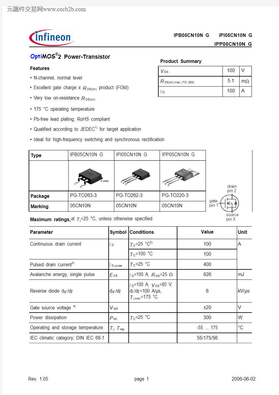
Opti MOS ?Unit Value PG-TO263-3PG-TO262-3PG-TO220-3
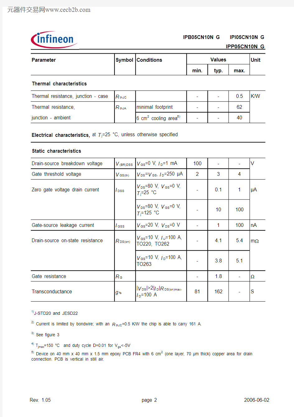
Parameter
Symbol Conditions
Unit
min.
typ.
max.
Thermal characteristics
Thermal resistance, junction - case R thJC --0.5K/W
Thermal resistance,R thJA
minimal footprint --62junction - ambient
6 cm 2 cooling area 5)
--40
Electrical characteristics, at T j =25 °C, unless otherwise specified Static characteristics
Drain-source breakdown voltage V (BR)DSS V GS =0 V, I D =1 mA 100--V
Gate threshold voltage V GS(th)V DS =V GS , I D =250 μA 234Zero gate voltage drain current
I DSS
V DS =80 V, V GS =0 V, T j =25 °C
-0.1
1
μA V DS =80 V, V GS =0 V, T j =125 °C
-10100Gate-source leakage current I GSS V GS =20 V, V DS =0 V -1100nA Drain-source on-state resistance
R DS(on)
V GS =10 V, I D =100 A, TO220, TO262-
4.1
5.4
m ?
V GS =10 V, I D =100 A, TO263
- 3.8 5.1Gate resistance R G - 1.8-?Transconductance
g fs
|V DS |>2|I D |R DS(on)max , I D =100 A
81
162
-S
1)J-STD20 and JESD22
5)
Device on 40 mm x 40 mm x 1.5 mm epoxy PCB FR4 with 6 cm 2 (one layer, 70 μm thick) copper area for drain connection. PCB is vertical in still air.
Values 4) T jmax =150 °C and duty cycle D=0.01 for V gs <-5V
2)
Current is limited by bondwire; with an R thJC =0.5 K/W the chip is able to carry 161 A.3) See figure 3
Parameter
Symbol Conditions
Unit
min.
typ.
max.
Dynamic characteristics Input capacitance C iss -905012000pF Output capacitance
C oss -13701820Reverse transfer capacitance C rss -75112Turn-on delay time t d(on)-2842ns
Rise time
t r -4263Turn-off delay time t d(off)-6496Fall time
t f
-
21
31
Gate Charge Characteristics 6)Gate to source charge Q gs -4661nC
Gate to drain charge Q gd -3248Switching charge Q sw -5173Gate charge total Q g -136181Gate plateau voltage V plateau - 5.1-V Output charge Q oss
V DD =50 V, V GS =0 V -
145
193
nC
Reverse Diode
Diode continous forward current I S --100A
Diode pulse current I S,pulse --400Diode forward voltage V SD V GS =0 V, I F =100 A, T j =25 °C - 1.0 1.2
V Reverse recovery time t rr -110ns
Reverse recovery charge
Q rr
-
360
-nC
6)
See figure 16 for gate charge parameter definition
V R =50 V, I F =I S , d i F /d t =100 A/μs
T C =25 °C
Values V GS =0 V, V DS =50 V, f =1 MHz
V DD =50 V, V GS =10 V, I D =50 A, R G =1.6 ?V DD =50 V, I D =100 A, V GS =0 to 10 V
5 Typ. output characteristics
1 Power dissipation
9 Drain-source on-state resistance
13 Avalanche characteristics
PG-TO220-3: Outline
PG-TO-263 (D2-Pak)
Published by
Infineon Technologies AG
81726 München, Germany
? Infineon Technologies AG 2006.
All Rights Reserved.
Attention please!
The information given in this data sheet shall in no event be regarded as a guarantee of conditions or characteristics (“Beschaffenheitsgarantie”). With respect to any examples or hints given herein, any typical values stated herein and/or any information regarding the application of the device, Infineon Technologies hereby disclaims any and all warranties and liabilities of any kind, including without limitation warranties of
non-infringement of intellectual property rights of any third party.
Information
For further information on technology, delivery terms and conditions and prices please contact your nearest Infineon Technologies Office (https://www.doczj.com/doc/8b3616564.html,).
Warnings
Due to technical requirements components may contain dangerous substances. For information on the types in question please contact your nearest Infineon Technologies Office.
Infineon Technologies Components may only be used in life-support devices or systems with the express written approval of Infineon Technologies, if a failure of such components can reasonably be expected to cause the failure of that life-support device or system, or to affect the safety or effectiveness of that device or system. Life support devices or systems are intended to be implanted in the human body, or to support and/or maintain and sustain and/or protect human life. If they fail, it is reasonable to assume that the health of the user or other persons may be endangered.