
Design and Implementation of Low-Profile Contactless Battery Charger Using Planar Printed Circuit Board Windings as
Energy Transfer Device
Byungcho Choi,Member,IEEE,Jaehyun Nho,Honnyong Cha,Taeyoung Ahn,Member,IEEE,and
Seungwon Choi,Member,IEEE
Abstract—This paper paper presents the practical details in-volved in the design and implementation of a contactless battery charger that employs a pair of neighboring printed circuit board (PCB)windings as a contactless energy transfer device.A proto-type contactless battery charger developed for application with cel-lular phones is used as an example to address the design consid-erations for the PCB windings and energy transfer circuit,plus demonstrates the performance of the contactless charger adapted to a practical application system.
Index Terms—Contactless battery charger for cellular phones, contactless energy transfer,coupled printed circuit board(PCB) windings.
I.I NTRODUCTION
E ARLIER studies[1]–[3]have shown that substantial
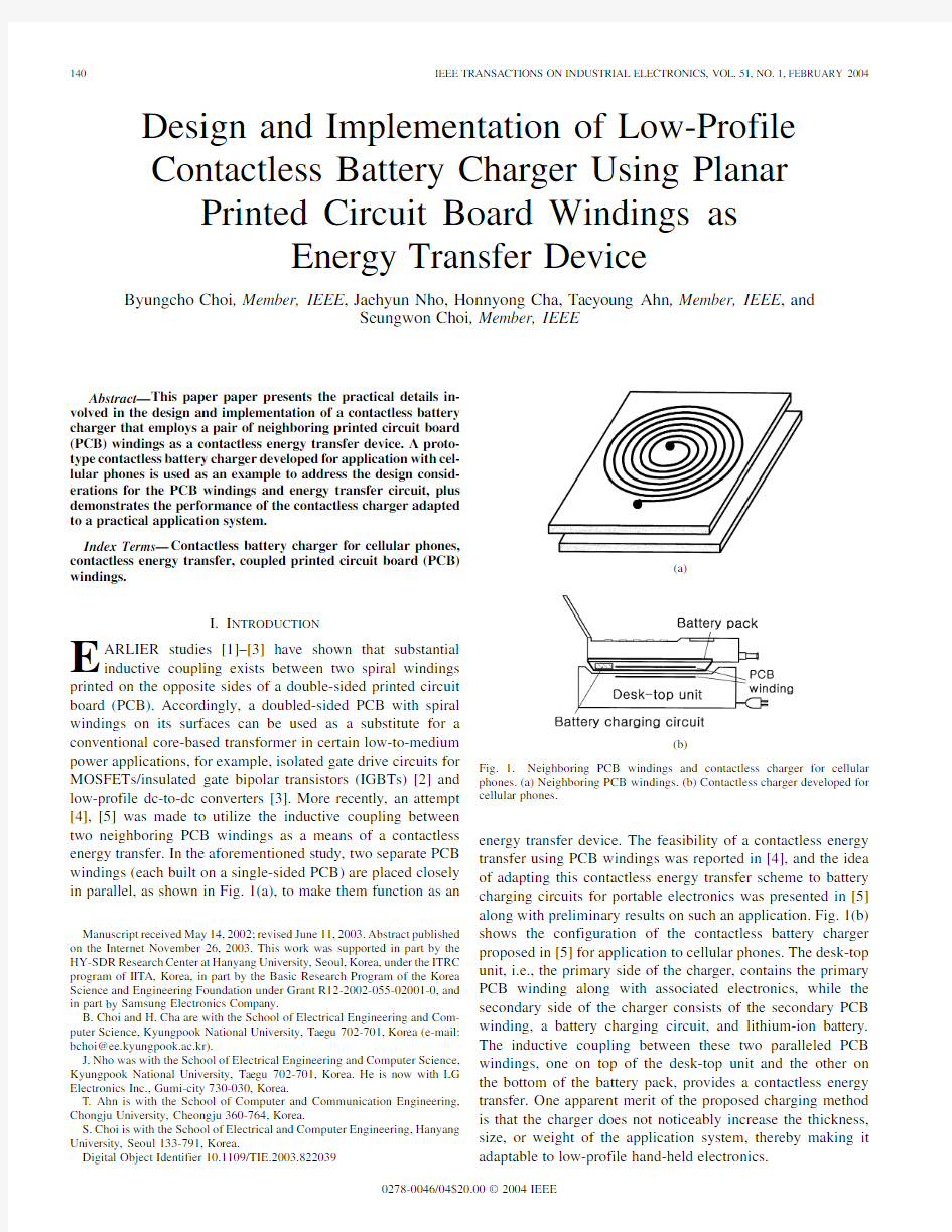
inductive coupling exists between two spiral windings printed on the opposite sides of a double-sided printed circuit board(PCB).Accordingly,a doubled-sided PCB with spiral windings on its surfaces can be used as a substitute for a conventional core-based transformer in certain low-to-medium power applications,for example,isolated gate drive circuits for MOSFETs/insulated gate bipolar transistors(IGBTs)[2]and low-profile dc-to-dc converters[3].More recently,an attempt [4],[5]was made to utilize the inductive coupling between two neighboring PCB windings as a means of a contactless energy transfer.In the aforementioned study,two separate PCB windings(each built on a single-sided PCB)are placed closely in parallel,as shown in Fig.1(a),to make them function as an
Manuscript received May14,2002;revised June11,2003.Abstract published on the Internet November26,2003.This work was supported in part by the HY-SDR Research Center at Hanyang University,Seoul,Korea,under the ITRC program of IITA,Korea,in part by the Basic Research Program of the Korea Science and Engineering Foundation under Grant R12-2002-055-02001-0,and in part by Samsung Electronics Company.
B.Choi and H.Cha are with the School of Electrical Engineering and Com-puter Science,Kyungpook National University,Taegu702-701,Korea(e-mail: bchoi@ee.kyungpook.ac.kr).
J.Nho was with the School of Electrical Engineering and Computer Science, Kyungpook National University,Taegu702-701,Korea.He is now with LG Electronics Inc.,Gumi-city730-030,Korea.
T.Ahn is with the School of Computer and Communication Engineering, Chongju University,Cheongju360-764,Korea.
S.Choi is with the School of Electrical and Computer Engineering,Hanyang University,Seoul133-791,Korea.
Digital Object Identifier
10.1109/TIE.2003.822039
(a)
(b)
Fig. 1.Neighboring PCB windings and contactless charger for cellular
phones.(a)Neighboring PCB windings.(b)Contactless charger developed for
cellular phones.
energy transfer device.The feasibility of a contactless energy
transfer using PCB windings was reported in[4],and the idea
of adapting this contactless energy transfer scheme to battery
charging circuits for portable electronics was presented in[5]
along with preliminary results on such an application.Fig.1(b)
shows the configuration of the contactless battery charger
proposed in[5]for application to cellular phones.The desk-top
unit,i.e.,the primary side of the charger,contains the primary
PCB winding along with associated electronics,while the
secondary side of the charger consists of the secondary PCB
winding,a battery charging circuit,and lithium-ion battery.
The inductive coupling between these two paralleled PCB
windings,one on top of the desk-top unit and the other on
the bottom of the battery pack,provides a contactless energy
transfer.One apparent merit of the proposed charging method
is that the charger does not noticeably increase the thickness,
size,or weight of the application system,thereby making it
adaptable to low-profile hand-held electronics.
0278-0046/04$20.00?2004IEEE
Fig.2.Simplified circuit diagram of proposed contactless charger.
As an extension and supplement to earlier publications[4], [5],the current paper presents the practical details involved in the design and implementation of the proposed contactless bat-tery charger.Section II addresses the general design considera-tions for the application circuit of the coupled PCB windings, then the circuit topology adapted to the prototype charger is presented.A series of design-oriented analyses of the proposed contactless charger are performed in Section III,along with the development of a linear circuit model for the contactless charger and its subsequent use to establish a design method for the proto-type charger.Finally,Section IV demonstrates the operation and performance of the prototype charger,thereby substantiating the application potential of the contactless charging scheme using neighboring PCB windings.
II.C ONTACTLESS B ATTERY C HARGER
As an energy transfer device,the function of coupled PCB windings is essentially identical to that of a conventional trans-former.However,due to the presence of a separation and the absence of a magnetic core between the PCB windings,cou-pled PCB windings exhibit unique device properties.As will be detailed in Section III,coupled PCB windings can be con-sidered as a transformer with a large leakage inductance and small magnetizing inductance.A large leakage inductance can incur a substantial increase in the power loss,component stress, and switching noise in the application circuit[6],[7].To re-solve this problem,the application circuit can employ resonant or soft-switching converter topologies that absorb the leakage inductance as a circuit component.Conversely,a small mag-netizing inductance causes a large current to circulate within the application circuit.In turn,this large circulating current in-duces significant conduction losses at parasitic components in the application circuit,particularly an excessive ohmic loss at the cupper traces of the PCB windings.Accordingly,certain de-sign considerations need to be incorporated in the application circuit to restrict the circulating current to an acceptable level. Fig.2shows a simplified circuit diagram of the proposed con-tactless battery charger.The desk-top unit consists of a line-fre-quency rectifier,high-frequency inverter,and the primary PCB winding.A half-bridge series resonant circuit is selected for the inverter topology as it utilizes the leakage inductance of the PCB windings as an element of the resonant tank circuit.The use of a resonant circuit also has advantages in that it minimizes the harmonic components in the circuit waveforms,thereby easing the electromagnetic interference(EMI)problem that can be in-curred by the PCB windings in operation.In addition,a half-bridge series resonant circuit readily achieves a high-frequency operation,which is essential to reduce the circulating current.
A conventional step-down
transformer,,is inserted between the half-bridge switch network and the resonant tank circuit to further reduce the circulating current.
The secondary side of the charger includes the secondary PCB winding,a high-frequency rectifier,and battery-charging circuit.The battery charging circuit is designed using an LT1571-5[8],which contains all the power switches, pulsewidth-modulation block,feedback control circuit,and other circuits needed to monitor and control the charging current.The battery charging circuit employs a synchronous buck converter to enhance its efficiency.In this particular application,it was possible to miniaturize the secondary side of the charger to the extent that the entire secondary part of the charger was installed inside the battery pack.
The desk-top unit operates in an open-loop condition and all the functions required to monitor and control the charging cur-rent are implemented in the battery charging circuit.Accord-ingly,the desk-top unit and secondary side of the charger are fully isolated in their functions,thereby eliminating the need for an additional information exchange[9]between them.The operational conditions and circuit parameters of the prototype charger are summarized in Table I.As shown in Table I,the output voltage of the high-frequency rectifier should remain within an
820-V range to ensure the reliable operation of the LT1571-5used in the battery-charging circuit.
III.D ESIGN-O RIENTED A NALYSIS
This section presents the modeling,analysis,and design of the proposed contactless battery charger.Based on the circuit analysis results,a design method is established that offers ef-ficient operation for the proposed charger under all operating conditions.
A.PCB Windings and Circuit Model
Table II shows the physical and electrical parameters of the PCB windings used in the prototype charger.The PCB wind-ings are fabricated on a single-sided PCB with a1-mm laminate thickness and3-oz/ft cupper layer.The dimensions and geom-etry of the cupper traces are empirically determined considering the operating conditions of the charger and circuit properties of the PCB windings.Since the power-handling capacity of the PCB windings is proportional to the area of the cupper traces[2], the size of the PCB windings should be designed according to the power requirements of the application system.In the current design,however,the PCB windings are oversized in an attempt to ensure the continuous operation of the battery charger even with a considerable misalignment between the PCB windings. Details on this point are presented in Section III-C.The35-mm-diameter spiral PCB windings used in the prototype charger were in fact tested to deliver a24-W output power at a68% efficiency with the cupper traces2.4mm apart.The geometry of the cupper traces directly affects the circuit properties of the PCB windings.Many turns of thin cupper traces enhances the inductive parameters of the PCB windings,however,this de-sign also increases the winding resistances.Therefore,the turns and width of the cupper traces were designed based on an ex-
TABLE I
O PERATIONAL C ONDITIONS AND C IRCUIT P ARAMETERS OF P ROTOTYPE C
HARGER
TABLE II
P HYSICAL AND E LECTRICAL P ARAMETERS OF PCB W
INDINGS
perimental tradeoff study on the performance of the PCB wind-ings in the prototype charger.The effects of the dimension and patterns of cupper traces on the properties of neighboring PCB windings were covered in [10].
Fig.3shows a circuit model for the neighboring PCB wind-ings.The circuit model is developed using the conventional method [11]that has been used to model magnetically coupled
inductors.Referring to Fig.3,the inductive
parameter
is re-ferred to as the leakage inductance,
while
is called the mag-netizing inductance,following the terminologies used to quan-tify the nonideal characteristics of conventional transformers.The circuit parameters shown in Fig.3can be either analytically calculated [12]or experimentally measured [2].The model pa-rameters measured from the PCB windings separated from each other by 2.4mm (the laminate thickness of the two PCBs plus a 0.4-mm distance between the PCBs)are listed in Table II.In-terestingly,the leakage
inductance,
H,is
larger Fig.3.Circuit model for neighboring PCB windings.
than the magnetizing
inductance,H.These unique
characteristics are attributed to the existence of a separation and the absence of a magnetic core between the PCB windings.The
winding
resistances,
,are also important circuit parameters as the ohmic loss in the PCB windings can be a major source of power losses.
Fig.4.Linear circuit model of proposed battery charger.
TABLE III
C IRCUIT V ARIABLES AN
D P ARAMETERS FOR C IRCUIT M ODEL
OF
C ONTACTLESS C
HARGER
B.Circuit Model for Battery Charger
Fig.4shows a linear circuit model for the proposed con-tactless charger.The model is created by adapting the circuit model of the PCB windings to the well-known modeling tech-nique [13],[14]for resonant converters.The model consists of three stages.The first stage is a dc model that represents the dc characteristics of the line-frequency rectifier and half-bridge switch network.The second stage is an ac model that describes the relationships between the fundamental components of the circuit variables associated with the PCB windings,based on the assumption that the higher order harmonics of the circuit vari-ables are well suppressed by the resonant tank circuit thus only the fundamental components are present in the circuit.The third stage models the functional behavior of the battery charging cir-cuit.The third stage terminates with an equivalent load resistor,
given
by
with representing the output voltage of the high-frequency rectifier
and
denoting the input cur-rent to the battery charging circuit.The typical operating point
of the battery charging circuit is located
at
V
and A,thereby resulting
in .The expressions
for the circuit variables and parameters appearing in Fig.4are given in Table
III.
Fig.5.Output voltage of high-frequency rectifier.(a)Output voltage with different line voltages.(b)Output voltage with different gaps.(c)Output voltage with different distances.
C.Voltage Transfer Gain of Contactless Charger
In this section,the voltage transfer gain of the contactless charger is analyzed using its linear circuit model.The results of the analysis are then used to determine the switching frequency of the prototype charger.From Fig.4,the voltage transfer gain from the line voltage to the output voltage of the high-frequency rectifier can be recognized
as
(1)
Fig.6.Collection of output voltage
curves.
Fig.7.Current and voltage waveform of primary PCB winding.(a)Current:2A/div,400ns/div.(b)V oltage:10V/div,400ns /div.
Using the expressions given in Table III,the voltage transfer gain can be evaluated
as
(2)
where is the input-to-output transfer function of the
second-stage ac model.By
evaluating
,the magni-tude of the voltage transfer gain can be expressed as a function of the switching
frequency
(3)
Equation (3)can now be used to predict the output voltage of the high-frequency rectifier under various operating conditions.Fig.5(a)shows the output voltage curves evaluated when the
line voltage varies
from
V
to V
while
(a)
(b)
Fig.8.Secondary side of prototype contactless charger developed for cellular phones.(a)Secondary side of charger.(b)Cellular phone equipped with secondary side of charger.
the separation between the PCB windings is fixed at 2.4mm.
Each theoretical curve is compared with experimental data mea-sured using the prototype charger in which the output terminals of the high-frequency rectifier are connected to a
45-resistor.Since theoretical transfer curves are only valid for frequencies above the resonance frequency of the LC tank [13],the curves are experimentally verified at frequencies higher than 600kHz.The experimental data exhibit a good correlation with the ana-lytical predictions,thereby validating the modeling and analysis method.
Fig.5(b)shows the output voltage curves evaluated when the separation between the PCB windings is varied
between
mm
gap mm [the definition for “gap ”is shown in
Fig.5(b)],while the line voltage is fixed
at
V.Each theoretical curve is obtained by evaluating (3)using the circuit parameters measured with a different separation between the
(a)
(b)
(c)
Fig.9.
Prototype charger and its performance.(a)Prototype charger in operation.(b)Charging profile.(c)Efficiency.
PCB windings.Fig.5(c)shows the analysis results of the circuit in which the separation is fixed at 2.4mm and the line voltage
set
at
V,yet the cupper traces are off center due to the misalignment of the PCB windings.Fig.5(c)shows the output voltage curves when the lateral distance between the centers of
the cupper traces is varied
between
mm
distance
mm;the definition for “distance ”is illustrated in Fig.5(c).
As emphasized in Section II,the output voltage of the high-frequency rectifier should be limited within an
820-V range for a stable operation of the control IC inside the battery charging circuit.Fig.6shows a collection of all the output voltage curves analyzed in Fig.5(a)–(c).As illustrated in Fig.6,when the switching frequency is set at a frequency within a
920980-kHz range,the output voltage of the high-frequency rectifier never exceeds the
820-V boundary.Based on this analysis,the switching frequency of the inverter is chosen to
be kHz.This design strategy provides a stable operation for the charger under all operating conditions without requiring an additional feedback path [9]between the desk-top unit and the secondary side of the charger.Since the switching frequency is selected well above the resonant frequency of the tank circuit,this design also provides a zero-voltage switching condition for the switch network [14]and offers high impedance characteristics for the resonant thank circuit [15],thereby reducing the circulating current in the circuit.
IV .P ERFORMANCE OF P ROTOTYPE C HARGER
This section describes the operation and performance of the prototype battery charger under various operating conditions.Fig.7shows the current and voltage waveform of the primary
PCB winding measured
when
V,,and with a 2.4-mm separation between the PCB windings.The current passing through the primary winding [Fig.7(a)]is al-most a sinusoidal wave.The voltage across the primary winding [Fig.7(b)]is also smoothly filtered by the inductances of the PCB windings.As such,these continuous and smooth wave-forms alleviate the possible EMI problems associated with the PCB windings in operation.
Fig.8(a)shows the secondary side of the prototype charger fabricated on a double-sided PCB.A 3.3-W lithium-ion battery along with the battery-charging circuit is placed on the front side,while the secondary PCB winding is printed on the oppo-site side.Fig.8(b)shows a cellular phone equipped with the sec-ondary side of the prototype charger.As shown in Fig.8(b),the secondary side of the charger is naturally suited for a low-pro-file design and therefore can readily be encapsulated within a standard battery pack without causing any major heat manage-ment problems.
Fig.9(a)shows the proposed contactless charging system in operation.The prototype charger was not found to have any
adverse effect on the performance of the cellular phone.No perceptible consequences of EMI were observed during the field tests,however,a newly proposed shielding technique[3] using a ferrite polymer composite sheet could be adapted for PCB windings to suppress the leakage flux to a negligible level. Fig.9(b)shows the charging characteristics of the prototype charger that goes through a transition from constant-current charging to constant-voltage charging.The charger exhib-ited a precisely controlled charging profile.Fig.9(c)shows the efficiency of the proposed charger measured under two different conditions:constant-current charging[upper curve in Fig.9(c)]and constant-voltage charging[lower curve in Fig.9(c)].A maximum efficiency of57%was measured during the constant-current charging mode.In these measurements,a dc voltage source was used as a substitute for the rectified line voltage.
V.C ONCLUSION
This paper has demonstrated a practical contactless charger, applicable to most low-profile hand-held electronics as well as cellular phones,which is implemented using two neighboring PCB windings as the energy transfer device.The efficient oper-ation of the prototype contactless charger was also confirmed, even with a considerable separation and misalignment between the PCB windings,when the PCB windings,energy transfer cir-cuit,and battery charging circuit were systematically and har-moniously designed.The main features of the prototype charger presented in this paper are summarized below.
?The secondary side of the charger is fabricated in a low-profile fashion,thereby allowing the entire secondary part of the charger to be encapsulated within a standard battery pack.
?The power loss in the prototype charger is kept at a low level to avoid any major thermal problems.A series res-onant circuit is used for the energy transfer circuit and
a synchronous buck converter is adapted for the battery
charging circuit to minimize the power losses.
?The prototype charger does not necessitate any informa-tion feedback between the primary and secondary side of the charger.This significantly simplifies the design and operation of the charger,when compared to other contact-less chargers that require a feedback path to control the battery charging current.
?The prototype charger does not cause any perceptible EMI problems,primarily due to the use of a series resonant circuit that generates continuous and smooth waveforms with negligible high-frequency harmonic components.
A CKNOWLEDGMENT
The authors gratefully acknowledge the technical support provided by Samsung Electronics Company during the course of this research.
R EFERENCES
[1]S.Y.R.Hui,S.C.Tang,and H.Chung,“Coreless printed-circuit board
transformers for signal and energy transfer,”Electron.Lett.,vol.34,no.
11,pp.1052–1054,1998.
[2],“Optimal operation of coreless PCB transformer-isolated gate
drive circuit with wide switching frequency range,”IEEE Trans.Power Electron.,vol.14,pp.506–514,May1999.
[3]S. C.Tang,S.Y.R.Hui,and H.Chung,“A low-profile power
converter using printed-circuit board(PCB)power transformer with ferrite polymer composite,”IEEE Trans.Power Electron.,vol.16,pp.
493–498,July2001.
[4] B.Choi and J.Nho,“Contactless energy transfer using planer printed
circuit board windings,”Electron.Lett.,vol.37,no.16,pp.1007–1009, 2001.
[5] B.Choi,H.Cha,J.Nho,and S.Park,“A new contactless battery charger
for portable telecommunication/computing electronics,”in Proc.IEEE ICCE’01,June2001,pp.58–59.
[6] D.G.Pedder,A.D.Brown,and J.A.Skinner,“A contactless electrical
energy transmission system,”IEEE Trans.Ind.Electron.,vol.46,pp.
23–30,Feb.1999.
[7]Y.Jang and M.Jovanivic,“A contactless electrical energy transmission
system for portable-telephone battery chargers,”in Proc.INTELEC’00, 2000,pp.726–732.
[8]“LT1572data sheet,”Linear Technology Co.,Milpitas,CA,2000.
[9] C.Kim,D.Seo,J.You,J.Park,and B.H.Cho,“Design of a contact-
less charger for cellular phone,”IEEE Trans.Ind.Electron.,vol.48,pp.
1238–1247,Dec.2001.
[10] C.Fernandez,O.Garcia,R.Prieto,J.A.Cobos,S.Gabriels,and G.Van
Der Borght,“Design issues of a coreless transformer for a contactless application,”in Proc.APEC’02,2002,pp.339–345.
[11]J.W.Nilsson and S.A.Riedel,Electronic Circuits,6th ed.Upper
Saddle River,NJ:Prentice-Hall,2001,pp.993–1001.
[12]W.G.Hurley and M.C.Duffy,“Calculation of self and mutual induc-
tances in planar magnetic structures,”IEEE Trans.Magn.,vol.31,pp.
2416–2422,July1995.
[13]R.L.Steigerwald,“A comparison of half-bridge resonant converter
topologies,”IEEE Trans.Power Electron,vol.3,pp.174–182,Apr.
1988.
[14]R.W.Erickson and D.Maksimovic,Fundamentals of Power Elec-
tronics,2nd ed.Norwell,MA:Kluwer,2001,ch.19.
[15]M.K.Kazimierczuk and T.Nandakumar,“Class D voltage switching
inverter with tapped resonant inductor,”Proc.Inst.Elect.Eng.,pt.B, vol.140,no.3,pp.177–185,May
1993.
Byungcho Choi(S’90–M’91)received the B.S.de-
gree in electronics from Hanyang University,Seoul,
Korea,in1980,and the M.S.and Ph.D.degrees in
electrical engineering from Virginia Polytechnic In-
stitute and State University,Blacksburg,in1988and
1992,respectively.
From1992to1993,he was a Research Scientist
with the Bradley Department of Electrical Engi-
neering,Virginia Polytechnic Institute and State
University.From1994to1995,he served as a Team
Leader of the Power Electronics Systems Team at Samsung Electronics Company.In1996,he joined the School of Electronic and Electrical Engineering,Kyungpook National University,Taegu,Korea, where he is presently an Associate Professor.His research interests include modeling and design optimization of high-frequency power converters for portable electronics,computer power systems,and distributed power
systems.
Jaehyun Nho received the B.S.degree in electronic
engineering from Taegu University,Taegu,Korea,in
1994,and the M.S.degree in electrical engineering
from Kyungpook National University,Taegu,Korea,
in2002.
He is presently with LG Electronics,Gumi-city,
Korea,where he is involved with the development
of power conditioning and driving circuits for ac
plasma display panel(PDP)application systems.His
research interests include modeling,analysis,and
design of low-profile power converters and driving circuits for large-diagonal PDP application systems.
Honnyong Cha received the B.S.and M.S.degrees in electrical engineering in 1999and 2001,respec-tively,from Kyungpook National University,Taegu,Korea,where he is currently working toward the Ph.D.degree.
From 2001to 2003,he was a Research Engi-neer with Power System Technology Company,Ansan-city,Korea,where he was involved with the development of power electronics application systems.His research interests include modeling,analysis,and design of resonant power conversion
circuits.
Taeyoung Ahn (M ’88)received the B.S.and M.S.degrees from Hanyang University,Seoul,Korea,in 1984and 1990,respectively,and the Ph.D.degree from Kyushu University,Kyushu,Japan,in 1994,all in electronics engineering.
In 1997,he joined the School of Computer and Communication Engineering,Chongju University,Cheongju,Korea,where he is currently an Assistant Professor.His main research interests include modeling,design,and performance evaluation of board-mount switching power converters for
telecommunication
applications.
Seungwon Choi (M ’91)received the B.S.degree in electronics engineering from Hanyang University,Seoul,Korea,in 1980,the M.S.degree in electronics engineering from Seoul National University,Seoul,Korea,in 1982,and the M.S.degree in computer engineering and the Ph.D.degree in electrical engineering from Syracuse University,Syracuse,NY ,in 1985and 1988,respectively.
From 1988to 1989,he was with the Department of Electrical and Computer Engineering,Syracuse Uni-versity,as an Assistant Professor.In 1992,he joined
Hanyang University as an Assistant Professor.He is currently a Professor in the School of Electrical and Computer Engineering.His research interests include digital communications and adaptive signal processing with a recent focus on the real-time implementation of the smart antenna systems for 3G mobile com-munication systems.
2016-2022年中国PCB药水行业深度 调研研究报告 https://www.doczj.com/doc/872389084.html,
什么是行业研究报告 行业研究是通过深入研究某一行业发展动态、规模结构、竞争格局以及综合经济信息等,为企业自身发展或行业投资者等相关客户提供重要的参考依据。 企业通常通过自身的营销网络了解到所在行业的微观市场,但微观市场中的假象经常误导管理者对行业发展全局的判断和把握。一个全面竞争的时代,不但要了解自己现状,还要了解对手动向,更需要将整个行业系统的运行规律了然于胸。 行业研究报告的构成 一般来说,行业研究报告的核心内容包括以下五方面:
行业研究的目的及主要任务 行业研究是进行资源整合的前提和基础。 对企业而言,发展战略的制定通常由三部分构成:外部的行业研究、内部的企业资源评估以及基于两者之上的战略制定和设计。 行业与企业之间的关系是面和点的关系,行业的规模和发展趋势决定了企业的成长空间;企业的发展永远必须遵循行业的经营特征和规律。 行业研究的主要任务: 解释行业本身所处的发展阶段及其在国民经济中的地位 分析影响行业的各种因素以及判断对行业影响的力度 预测并引导行业的未来发展趋势 判断行业投资价值 揭示行业投资风险 为投资者提供依据
2016-2022年中国PCB药水行业深度调研及发展趋 势研究报告 【出版日期】2016年 【交付方式】Email电子版/特快专递 【价格】纸介版:7000元电子版:7200元纸介+电子:7500元 【报告编号】R429020 【报告链接】https://www.doczj.com/doc/872389084.html,/research/201607/429020.html 报告目录: 我国市场上PCB药水以国外品牌居多,国内品牌较少,随着国家对PCB行业的重视,对PCB药水的环保要求越来越高。 面对国际宏观经济形势复杂多变,行业周期性回落等不利因素,加强技术创新,调整和优化PCB药水产品结构,重点开发高性能化、专用化、绿色化产品,已成为当前PCB药水发展的重要特征,也是今后我国PCB药水发展的重点方向。 2011年,全球最大笔电印刷电路板厂瀚宇博4月份正式调涨PCB 售价,欧洲最大的印制电路板制造商奥特斯宣布将加快在中国的投资步伐,建设更多的高端印制电路板生产线和生产基地,抢先布局中国市场。各大印刷电路板大厂纷纷出招,争夺PCB的利润,由此可见,2011年的PCB市场利润满满。 面对发展态势如此之好的下游市场,PCB药水的投资前景也非常广阔。
三极管流水灯电路设计 王雅 20111041105;韦梦娜 20111041107 摘要:3组12只LED流水灯是特别针对电子装配与调试技能设计出来的,值得学习和电路分析。本文分析了该流水灯电路的特点及其电路工作原理的说明。 关键字:3组12只LED流水灯;电路设计;循环。 1 引言 随着科学技术的发展,电力电子设备与人们的工作、生活的关系日益密切。各种小套件层出不穷,功能多样。本文所设计的电子制作可以说是电子初学者学习电子的最佳入门制作!其制作方式容易,趣味横生,更能提高初学者的动手能力!让初学者在制作学习中感受电子技术带来的乐趣! 2 系统的功能描述 这款3组12只LED流水灯具有制作容易、有趣易学的特点,电路焊接成功后,装入电池,即可正常工作,3组12只发光二极管便会被轮流点亮,不断的循环发光,达到流动的效果。 3 设计原理 3.1 电路工作原理说明: 本电路是由3只三极管组成的循环驱动电路。每当电源接通时,3只三极管会争先导通,但由于元器件存在差异,只会有1只三极管最先导通。这里假设V1最先导通,则V1集电极电压下降,使得电容C2的左端下降,接近0V。由于电容两端的电压不能突变,因此此时V2的基极也被拉到近似0V,V2截止,V2的集电极为高电压,故接在它上面的发光二极管LED5-LED8被点亮。此时V2的高电压通过电容C3使V3基极电压升高,V3也将迅速导通,因此在这段时间里,V1、V3的集电极均为低电压,因此只有LED5-LED8被点亮,LED1-LED4、LED9-LED12熄灭。但随着电源通过电阻R3对C2的充电,V2的基极电压逐渐升高,当超过0.7V时,V2由截止状态变为导通状态,集电极电压下降,LED5-LED8熄灭。与此同时,V2的集电极下降的电压通过电容C3使V3的基极电压也降低,V3由导通变为截止,V3的集电极电压升高,LED9-LED12被点亮。接下来,电路按照上面叙述的过程循环,3组12只发光二极管便会被轮流点亮,不断的循环发光,达到流动的效果。改变电容C1、C2、C3的容量可以改变循环速度,容量越小,循环速度越快。电源使用2节5号干电池即可。 3.2元件清单: 3.3 电路图
课程设计报告 利用Altium Designer设计单片机实验系统PCB板 学院城市轨道交通学院 专业电气工程与自动化 班级10控制工程 学号1042402057 姓名方玮 指导老师刘文杰 完成时间2013-05-21
目录 一、设计目的 (2) 二、设计方案 2.1、设计流程图 (2) 2.2、板层选择 (2) 2.3、元件封装 (3) 2.4、布线方案 (4) 三、原理图的绘制 3.1创建新的PCB工程 (4) 3.2创建新的电气原理图 (5) 3.3添加电路原理图到工程当中 (5) 3.4设置原理图选项 (5) 3.5电路原理图绘制 (6) 3.5.1 加载库和元件 (6) 3.5.2 放置元件 (7) 3.5.3 绘制电路 (9) 3.5.4 注意事项 (11) 3.6编译工程 (14) 四、PCB板的绘制 4.1创建新的PCB文件 (15) 4.2在工程中添加新的PCB (16) 4.3 将原理图的信息导入PCB (17) 4.4 PCB的绘制 (17) 4.4.1元件放置 (17) 4.4.2规则设置 (18) 4.4.3手动布线 (19) 4.4.4规则检查 (21) 五、实验心得体会 (23) 六、附录1 原理图 (24) 七、附录2 PCB图 (25)
利用Altium Designer 设计单片机实验 系统PCB板 一、设计目的 1.培养学生掌握、使用实用电子线路、计算机系统设计、仿真软件的能力。2.提高学生读图、分析线路和正确绘制设计线路、系统的能力。 3.了解原理图设计基础、了解设计环境设置、学习 Altium Designer 软件的功能及使用方法。 4.掌握绘制原理图的各种工具、利用软件绘制原理图。 5.掌握编辑元器件的方法构造原理图元件库。 6.熟练掌握手工绘制电路版的方法。 7.掌握绘制编辑元件封装图的方法,自己构造印制板元件库。 8.了解电路板设计的一般规则、利用软件绘制原理图并自动生成印制板图。 二、设计方案 2.1 设计流程图 2.2板层选择 根据层数分类,印制电路板可分为单面板、双面板和多层板。 (1)单面板 单面印制电路板只有一面有导电铜箔,另一面没有。在使用单面板时,通常在没有导电铜箔的一面安装元件,将元件引脚通过插孔穿到有导山铜箔的一面,导电铜箔将元件引脚连接起来就可以构成电路或电子设备。单面板成本低,但因为只有一面有导电铜箔,不适用于复杂的电子设备。 (2)双面板 双面板包括两层:顶层(Top Layer)和底层(Bottom Layer)。与单面板不同,双面板的两层都有导电铜箔,其结构示意图如图2-1所示。双面板的每层都
第七章印制电路板的设计与制作 印制电路板PCB(PrintedCircuitBoard)简称为印制板,是安装电子元器件的载体,在电子设计竞赛中应用广泛。 印制电路板的设计工作主要分为原理图设计和印制电路板设计两部分。在掌握了原理图设计的基本方法后,可以进入印制电路板设计,学习印制电路板的设计方法。 完成印制电路板设计,需要设计者了解电路工作原理,清楚所使用的元器件实物,了解PCB板的基本设计规范,才能设计出适用的电路板。 第一节印制电路板设计的基础知识 1. 印制电路板的类型 一般来说,印制电路板材料是由基板和铜箔两部分组成的。基板可以分无机类基板和有机类基板两类。无机类基板有陶瓷板或瓷釉包覆钢基板,有机类基板采用玻璃纤维布、纤维纸等增强材料浸以酚醛树脂、环氧树脂、聚四氟乙烯等树脂黏合而成。铜箔经高温、高压敷在基板上,铜箔纯度大于99.8%,厚度约在18~105μm。 印制电路是在印制电路板材料上采用印刷法制成的导电电路图形,包括印制线路和印刷元件(采用印刷法在基材上制成的电路元件,如电容器、电感器等)。 根据印制电路的不同,可以将印制电路板分成单面印制板、双面印制板、多层印制板和性印制板。 (1)单面印制板仅在一面上有印制电路,设计较为简单,便于手工制作,适合复杂度和布线密度较低的电路使用,在电子设计竞赛中使用较多。 (2)双层印制板在印制板正反两面都有导电图形,用金属化孔或者金属导线使两面的导电图形连接起来。与单面印制板相比,双面印制板的设计更加复杂,布线密度也更高。在电于设计竞赛中,也可以手工制作。 (3)多层印制板是指由三层或三层以上导电图形构成的印制电路板,导体图形之间由绝缘层隔开,相互绝缘的各导电图形之间通过金属化孔实现导电连接。多层印制电路板可实现在单位面积上更复杂的导电连接,并大大提升了电子元器件装配和布线密度,叠层导电通路缩短了信号的传输距离,减小了元器件的焊接点,有效地降低了故障率,在各导电图形之间可以加入屏蔽层,有效地减小信号的干扰,提高整机的可靠性。多层印制板的制作需要专业厂商。 (4)软性印制板也称为柔性印制板或挠性印制板,是采用软性基材制成的印制电路板。特点是体积小,质量轻,可以折叠、卷缩和弯曲,常用于连接不同平面间的电路或
反渗透海水淡化系统中的能量回收装置 按照工作原理,流体能量回收技术主要分为流体非直接接触式和流体直接接触式两大类。 一、流体非直接接触式技术 在非直接接触式流体能量回收装置中,高低压流体对需要借助叶轮和轴来传递能量,即以机械能作为流体能量传递的中间环节,故又称为机械能中介式技术。能量转换过程为压力能——机械能——压力能。 采用流体非直接接触式技术的典型装置类型有逆转泵型、佩尔顿型叶轮和水力透平等。这种技术的节能机理是在回收高压流体中的压力能的同时减少高压泵的提升压力差来降低 系统的能耗。 1.逆转泵和佩尔顿叶轮型 逆转泵和佩尔顿叶轮型装置的原理类似,属于外力驱动泵式装置,即其加压泵由外电机驱动,通过轴传递的能量为辅助形式。高压废流体驱动透平中的叶轮,通过传动轴与泵连接,为新鲜低压流体加压,做功后的高压废流体丧失能量后排出。下图为此类装置的能量传递示意图 2.水力透平装置与逆转泵及佩尔顿叶轮机型最大的区别在于其透平叶轮和泵体叶轮安 装在同一壳体中,用高压浓盐水直接冲击透平叶片,通过轴功直接驱动加压泵工作,并尽可能减少中间传动轴的机械能损失,从高压流体回收后的能量作为唯一驱动力驱动泵的工作。下图为此装置的示意图 二、流体直接接触正位移技术 这种技术的节能机理是在产量不变的情况下减少通过高压泵的流量的方式来降低系统
的能耗。它是高低压流体直接交换压力能,而不需要机械辅助装置,又称正位移技术,能量的转换过程为压力能——压力能。按照运动部件的类型,这类装置可分为活塞式功交换器和旋转式压力交换器两种。 1.活塞式功交换器 活塞式功交换器自身结构简单,高压流体通过活塞为低压流体加压,同时活塞还可有效防止高低压流体的混流,而且活塞本山阻力非常小,传递效率接近100%。下图为其结构示意图 2.旋转式压力交换器 旋转式压力交换器主要部件是一个无轴的转子,沿轴向开有数个孔道,高低压流体在孔道中交换能量,并依靠转子的连续转动实现系统的连续运行。
中国印制电路板行业概况研究-行业概况及市场前景 (一)行业概况和市场前景 1、印制电路板行业简介 印制电路板(Printed Circuit Board,PCB),又称印刷电路板,指在通用基材上按预定设计形成点间连接及印刷元件的印刷板,其主要功能是使各种电子零组件形成预定电路的连接,起中继传输的作用。印制电路板被称为“电子系统产品之母”, 几乎所有的电子设备都要使用印制电路板,不可替代性是印制电路板制造行业得以长久稳定发展的重要因素之一。 印制电路板的制造品质、工艺技术对电子产品的可靠性、功能性产生直接影响。PCB 板主要由线路与图形、介电层、导通孔、防焊油墨、丝印、表面处理层等构成,不同部件发挥的作用如下:
2、PCB 产品分类 印制电路板分类方法较多,行业中应用较多的分类方法主要为以下几种:(1)按导电图形层数分类。 印制电路板按照导电图形层数可以分为:单面板、双面板和多层板。 单面板是最基本的印制电路板,元器件集中在其中一面,导线则相对集中在 另一面。 双面板是指在两面都有布线,并且在两面间有适当的电路连接的印制电路板,解决了单面板中布线交错的问题,可以用于较复杂的电路上。 多层板是指有四层及以上的导电图形的PCB,多层板的层数通常为偶数,层数越高所需的技术要求也越高,可以支持的功能也更丰富。 (2)按板材的材质分类 按PCB 使用的板材材质可以分为刚性板、挠性板、刚挠结合板。 刚性板是由不易弯曲、具有一定强韧度的刚性基材制成的印制电路板,在电子产品中得到广泛使用。刚性板的基材通常采用玻纤布基板、热塑性基板、复合基板、陶瓷基板、金属基板、纸基板等。 挠性板指采用柔性的绝缘基材制成的印制电路板,可根据安装要求进行弯曲、卷绕、折叠。挠性基材包括聚酰亚胺基板、聚酯基板等。 刚挠结合板是由刚性板和挠性板有序地层压组成,并以金属化孔形成电气连接,既可以提供刚性板的支撑作用,又具有挠性板的弯曲性,能够满足三维组装的要求。刚挠结合板对节省产品内部空间,减少成品体积,提高产品性能有很大的帮助。 (3)按技术、工艺等维度分为HDI 板和特殊板等。
流水灯电路的制作 一、概述: 随着电子技术的快速发展尤其是数字技术的突飞猛进,多功能流水灯凭着简易,高效,稳定等特点得到普遍的应用。在各种娱乐场所、店铺门面装饰、家居装潢、城市墙壁更是随处可见,与此同时,还有一些城市采用不同的流水灯打造属于自己的城市文明,塑造自己的城市魅力。目前,多功能流水灯的种类已有数十种,如家居装饰灯、店铺招牌灯等等。所以,多功能流水灯的设计具有相当的代表性。 多功能流水灯,就是要具有一定的变化各种图案的功能,主要考察了数字电路中一些编码译码、计数器原理,555定时器构成时基电路,给其他的电路提供时序脉冲,制作过程中需要了解相关芯片(NE555、CD4017)的具体功能,引脚图,真值表,认真布局,在连接过程中更要细致耐心。 二、电路原理图 三、电路工作原理 多功能流水灯原理电路图如上图所示。原理电路图由振荡电路、译码电路和光源电路三部分组成。本文选用的脉冲发生器是由NE555与R2、R3及C1组成的多谐振荡器组成。主要是为灯光流动控制器提供流动控制的脉冲,灯光的流动速度可以通过电位器R3进行调节。由于R3的阻值较大,所以有较大的速度调节范围。灯光流动控制器由一个十进制计数脉冲分配器CD4017和若干电阻组成。 CD4017的CP端受脉冲发生器输出脉冲的控制,其输出端(Q0~Q9)将输入脉冲按输入顺序依次分配。输出控制的脉冲,其输出控制脉冲的速度由脉冲发生器输出的脉冲频率决定。10
个电阻与CD4017的10个输出端Q0~Q9相连,当Q0~Q9依次输出控制脉冲时10个发光二极管按照接通回路的顺序依次发光,形成流动发光状态,即实现正向流水和逆向流水的功能。电源电路所采用的电源为。 四、板的设计 五、元器件清单 六、电路的组装与调试 1、电路的组装方法和步骤 (1)筛选元器件。对所有购置的元器件进行检测,注意它们的型号、规格、极性,应该保质量。 (2)按草图在PCB板上组装并焊接。 要求:①元器件布局整齐、美观,同类型元器件高度一致;
PCB手工制作详细教程 作者:冰檐化雨 绪言 相信电子爱好者们在电子制作过程中,最苦恼的就是电路板的制作了:如果用万能板做,看上去不是很入眼;如果把PCB稿图拿去工厂加工,单片板也得要几十。所以很麻烦,现在给大家推荐一种手工制板方法:感光法制板。这种方法在众多手工制板方法中效果是最好的,成本也很作者:低。 最小焊盘:60mil(1.5mm) 最小线距:10mil(0.25mm) 最小孔径:30mil(0.76mm) 最多层数:双面板 最小线宽:15mil(0.38mm) 这些参数是本人建议大家在制板时使用的参数,并不是实验中所得最小值,实际上还可以得到更小值,只是难度会比较大,比如线宽可以到10mil,但是也只能保证局部的线,板子上的线都到10mil,就比较难了) 例图:
友情链接:冰檐电子 https://www.doczj.com/doc/872389084.html,/shop/view_shop.htm?asker=wangwang&shop_nick=iceeave 目录 1.绘制PCB稿图并打印菲林胶片 2.铜板的覆膜与曝光 3.显影 4.腐蚀 5.脱膜 6.增加阻焊绿油 7.钻孔 一.绘制PCB稿图并打印菲林胶片 首先要用PCB绘制软件绘制出PCB稿图,也就是EDA软件或PCB Layout 软件,一般有以下几种:Protel、Pads、Cadence allegro、Mentor WG。这里只介绍Protel的几种版本的使用方法,本教程默认读者是会使用Protel软件的。关于PCB
的绘制不多说,直接介绍关于打印在菲林纸上的电路图案,菲林纸和一般的A4白色打印纸的唯一区别是菲林是透明的,也称为菲林胶片,菲林的两面只有一面是打印面,你用手摸上去感觉有些粗糙,喷墨打印机使用专用的喷墨菲林。下面是PCB 稿图(双直流稳压电源),但是这不能直接打印,还应该处理图1-1的样子。 至于为什么要处理成这样,这个后面再说,我先说这两个图的差别。可见菲林图案是黑白图案,上面只有走线、焊盘、铺铜、文字,而且白色部分是最后板子做出来后留在板子上的部分,黑色的都是不需要的,应该腐蚀掉的(PCB手工制板的
Recuperator能量回收装置 毋庸置疑,阿科凌与业内竞争对手相比的最大优势在于我们的专利设备— Recuperator能量回收装置。它是阿科凌专有的能量回收装置/工作转换机,阿科凌也因此成为全球唯一一家拥有专有能量回收装置的海水淡化水供应商。回流机属于等压能量回收装置,具体而言,它是一种活塞式工作转换机。 回流机结构紧凑,呈塔状结构,经过不断的改良, 如今已是第三个版本。阿科凌研发实验室不遗余力 地致力于回流机新功能的开发,并将于近期推出升 级版新产品。回流机目前仅应用于阿科凌的交钥匙 解决方案和自建自营的项目中,但计划不久将作为 第三方产品进行销售。回流机能实现高达98.5% 的废弃能量回收率,可大幅节省运营成本。 背景介绍 膜组件是反渗透海水淡化过程的核心部分,从一开 始,反渗透法海水淡化技术便致力于膜组件的开发 与改良。 阿科凌专功膜法脱盐项目,反渗透海水淡化过程的终极目标是获取材质与结构均符合脱盐市场需求(如高产出率、高脱盐率、抗高压、抗化学性和低给水污染物排放)的膜组件。 随着阿科凌系统设计技术的不断进步,加之阿科凌多年的反渗透系统运营经验、优化的预处理解决方案以及更高效设备和更优材质的采用,将成功节省运营成本并大幅降低系统的生命周期成本。 工作原理 回流机通过反渗透膜滤过的盐水给预处理海水加 压,加压过程由反渗透膜的盐水流量进行调节。 该装置包含两个直立的双向不锈钢塔,分别进行加 压转移和解压释放处理。预处理海水来自加压给水 箱,而给水箱为系统提供恒定的水流量和水压。 回流机能够将加压盐水的能量回收至反渗透膜及 增压泵—只需把加压盐水替换成相同流速的预处 理海水。
PCB(印刷线路板)行业链分析 (Printedcircuitboard,简称PCB)是组装电子零件用的基板,是在通用基材上按预定设计形成点间连接及印制组件的印制板。该产品的主要功能是使各种电子零组件形成预定电路的连接,起中继传输的作用,是电子产品的关键电子互连件。印刷线路板的制造品质,不但直接影响电子产品的可靠性,而且影响系统产品整体竞争力,因此印刷电路板被称为“电子系统产品之母”。印刷电路板产业的发展水平可在一定程度上反映一个国家或地区电子产业的发展速度与技术水准。 玻纤纱:玻纤纱由硅砂等原料在窑中煅烧成液态,通过极细小的合金喷嘴拉成极细玻纤,再将几百根玻纤缠绞成玻纤纱。窑的建设投资巨大,为资本密集型产业,3万吨的窑炉需要4亿人民币,新建窑炉需要18个月,景气周期难以掌握,且一旦点火必须24小时不间断生产,而且过五年左右,必须停产半年维修,进入退出成本巨大。 玻纤布:玻纤布是覆铜板的原材料之一,由玻纤纱纺织而成,约占覆铜板成本的40%(厚板)和25%(薄板)。玻纤布制造则和织布企业类似,可以通过控制转速来控制产能及品质,且规格比较单一和稳定,自二战以来几乎没有规格上的太大变化。和CCL 不同,玻纤布的价格受供需关系影响最大,最近几年的价格在0.50~1.00美元/米之间波动。目前台湾和中国内地的产能占到全球的70%左右。上下游的关系为营运关键,一台织布机的价格为10~15万,一般为100多台可正常生产,但后续的热处理和化学处理设备的资金要求较高,达千万级,织布的产能扩充容易,比较灵活。 铜箔:铜箔是占覆铜板成本比重最大的原材料,约占覆铜板成本的30%(厚板)和50%(薄板)以上,因此铜箔的涨价是覆铜板涨价的主要驱动力。铜箔的应用较广,不单应用于覆铜板行业,当覆铜板行业不景气时,铜箔厂商可以转产其他用途的铜箔。铜箔的价格密切反映于铜的价格变化,随着铜价的节节高涨,铜箔厂商把成本压力向下游转移。铜箔产业的高技术壁垒导致国内供给不足,高档铜箔仍需大量进口,投资办厂的成本也很大。 覆铜板(简称CCL):是以电子级玻璃纤维布为基材,浸以环氧树脂,经烘干处理后,制成半固化状态的粘结片,再在单面、双面或多层板面敷上板薄的铜箔,经特殊的热压工艺条件下制成的,是PCB的直接原材料。覆铜板行业资金需求量较大,规模小的厂大约为5000万元左右,集中度较高,全国有100家左右。覆铜板行业是成本驱动的周期性行业,在上下游产业链结构中,CCL对PCB的议价能力较强,只要下游需求尚可,就可将成本上涨的压力转嫁下游PCB厂商,但只有规模超大的CCL能在玻纤布、铜箔等原材料采购中拥有较强的话语权。由于覆铜板的产品用途单一,只能卖给印刷线
单片机课程设计 2014年 6月 15日 课 程 单片机课程设计 题 目 花样流水灯 院 系 电气工程及其自动化系 专业班级 1112班 学生姓名 温亿锋 学生学号 201111631227 指导教师 张瑛
一丶任务 设计一款以AT89C51单片机作为主控核心,按键控制电路、流水灯显示电路以及单片机最小系统等模块组成的核心主控制电路。 二丶设计要求 通过发光二极管显示不同的花样(至少有六种花样),并且可以通过按键来控制流水灯的速度。 三丶设计方案 本方案主要是通过对基于单片机的多控制、多闪烁方式的LED流水灯循环系统的设计,来达到本设计的要求。其硬件构成框图如下图所示,以单片机为核心控制,由单片机最小系统(时钟电路、复位电路、电源)、按键控制电路、LED 发光二极管和5V直流电源组成。 单片机流水灯循环控制系统硬件框图 此设计方案中单片机的P1口接5路按键控制电路,实现流水灯花型的切换功能;单片机的P3.7引脚接上一个按钮开关以实现对流水灯闪烁频率的控制,即实现了快慢两种节拍实现花型的变换;单片机上的P2口接八路LED发光二极管组成流水灯电路,显示流水灯循环情况。 四丶系统硬件设计 4.1 直流稳压电源电路
对于一个完整的电子设计来讲,首要问题就是为整个系统提供电源供电模块,电源电路的稳定可靠是系统平稳运行的前提和基础。电子设备除用电池供电外,还采用市电(交流电网)供电。通过变压、整流、滤波和稳压后,得到稳定的直流电。直流稳压电源是电子设备的重要组成部分。本项目直流稳压电源为+5V。 直流稳压电源的制作一般有3种制作形式,分别是分立元件构成的稳压电源、线性集成稳压电源和开关稳压电源。下图为稳压电源采用的是三端集成稳压器7805构成的正5V直流电源。 三端固定式集成稳压电源电路图 AT89C51单片机的工作电压范围:4.0V---5.5V,所以通常给单片机外接5V 直流电源。此处用3节1.5V的干电池供电。 4.2 单片机最小系统 要使单片机工作起来,最基本的电路的构成由单片机、时钟电路、复位电路等组成,单片机最小系统如图所示。 时钟电路:本系统采用单片机内部方式产生时钟信号,用于外接一个12MHz 石英晶体振荡器和2个30pF微调电容,构成稳定的的自激振荡器,其发出的脉冲直接送入内部的时钟电路。 复位电路:确定单片机工作的起始状态,完成单片机的启动过程。单片机系统的复位方式有上电自动复位和手动按键复位。本设计采用手动按键复位,该复位方式同样具有上电自动复位功能。
我来到大连XXX有限电子公司进行为期10周的实习培训。这里充满了和谐与朝气,充满了团结与智慧。本公司大连XX电子有限公司(简称:大连XX)主要从事二极管、MOSFET、肖特基等电子元器件的专业生产,以及PCB板的制作。公司总部设在辽宁大连庄河市,大连XX电子有限公司的诚信、实力和产品质量获得业界的认可。我的实习岗位是熟练运用protel制图软件并制成PCB板,并检验出制成的板质量是否合格。也就是进行PCB板的制作与维护。 1. 印制电路板的制作 实习过程中,我首先进行印制电路板的制作,具体步骤如下: 第一步,使用Protel设计PCB板。 首先,新建原理图库文件并设计:先要点击【Document】选择【schematic library】,在原来的库里找到类似的进行编辑修改,这样比较省时省力一些。找到相似的元件后我要注意,要把粘贴到【schematic library】里面进行的引脚等其他部分进行编辑和修改。设计完成后保存,回到【schematic document】中,找到自己做好的元件双击添加。 其次,新建原理图文件并设计:打开Protel 软件点击【New document】选择【schematic Document】,新建一个原理图纸,设置原理图图纸大小为“A4”。然后回到建好的原理图图纸页面,在任意位置,双击页面对照图纸来选择相应的符号,在原理图页面对照图纸画好原理图,双击的标示改好。在画原理图的时候特别要注意,导线的节点不能忘记标注,要修改属性,检查电气规则等。原理图中的集成电路,有些在库中找不到,需要自己画好添加到库中然后调用到原理图上。 然后,新建PCB文件并设计。在【New document】选择【PCB document】,将工作层面调至Keep Out Layer,并画出电路板电气边界。生成网络表后,打开网络表点击以NET 结尾的文件进行检查,检查错误,直到修改无误把焊盘修改为合适大小。之后导出并在电路板电气范围内排布,元件比较多排布元件比较麻烦,所以要与足够的耐心摆放元件以便最后出的图比较规整。手工布线清晰明了布线完成时要仔细检查。虽然经过一段很复杂的过程但当最后看见自己的成果时真的存在一种喜悦。然后设置点击【design
印制电路板手工制作方法与技巧 印制电路板(PCB板)是电子制作的必备材料,既起到元器件的固定安装作用,又起到元器件相互之间的电路连接作用,也就是说只要有元器件就一定需要PCB板,而PCB板不可能从市场上直接选购,一定要根据电子制作(电子产品)的不同需要单独生产制作。产品生产中的PCB板通常要委托专业生产厂家制作,但我们在科研、产品试制、业余制作、学生的毕设、课设大赛、创新制作等环节中只需一两块PCB板时,委托专业厂家制作,不仅时间长(一周左右或更长),费用高(百元以上),而且不便随时修改。电子制作中如何用最短时间(几十分钟)、最少费用(每平方厘米几分钱)、最简单的办法(一学就会)加工制作出精美的PCB板呢?下面向读者介绍几种简便易行的方法。 PCB板分单面板、双面板、多层板几种,在业余条件下只能实现单面和双面板印制板的制作。制作通常要经过如下几个环节: 设计准备覆铜板转移图形腐蚀钻孔表面处理 一、设计 把电路原理图设计成印制电路布线图,可在计算机上通过多种PCB设计软件实现。简单电路如可直接用手工布线完成,具体操作方法、要求、技巧等内容将在今后文章中详细介绍。 二、准备覆铜板 覆铜板是制作PCB板的材料,分单面覆铜板和双面覆铜板,铜箔板(厚度有18um、35um、55um和70um几种)通过专用胶热压到PCB基板上(基板厚度有0.2、0.5….1、1.6等几种规格),如图1所示。 制作中PCB板厚度根据制作需求选择,常用规格为1.6nm,铜箔厚度尽量选择薄的覆铜板,这样腐蚀速度快、侧蚀少,适合高精度PCB板的制作。覆铜板外形尺寸的大小与形状完全根据制作需求而定,可用剪板机、剪刀、锯等工具实现。 三、转印图形(或描绘) 将设计好的PCB布线图(包括焊盘与导线)转印(或描绘)到覆铜板上。本环节要求线条清晰、无断线、无砂眼、无短接,且耐水洗、抗腐蚀。 方法一:手工描绘法 (1)将设计好的PCB图按1:1画好,然后通过复写纸印到覆铜板上。
PCB行业基调 2016年,中国电子信息制造业规模约RMB12.2万亿,增速8.4%;利润总额6464亿元,同比增长16.1%;全球超2万亿美金规模以上 1、关键器件:IC 3389亿美元、显示屏1195亿美元、线路板656亿美元、等等 2、市场总量稳步增长,智能化、万物互联化之下的“电子+” 3、物理形态、结构可能会发生变化(SIP、新型材料),但“线路板”的本质属性不变 4、定制化的B-B产品不容易出现泡沫,无差异化的B-B会出泡沫,导致产能过剩。 5、高度分散的行业,CR5=20%,CR10=32%(定制原因) 一、市场规模&增速 预计 2018 年 PCB 产业同比成长 2%达到 560 亿美金,中国目前产值占50%的份额。(包含外资内地建厂) 二、细分品类结构 根据 Prismark 的预计,从 2016-2021 年 6 年复合增长率来看,增速最高的是柔性板 3%,其次是 HDI 板 2.8%,多层板 2.4%,单/双面板 1.5%,封装基板 0.1%。需求偏重高阶产品,FPC、HDI 板、多层板增速领先。新增产能扩产方向
三、历年下游应用分布及占比情况 下游核心需求集中在,通信、电子、汽车、计算机等领域。 四、全球市场格局 PCB产业正在不断向大陆迁移(覆盖这个行业的核心逻辑) PCB产业转移路径:美国(90年代顶峰)→日本(00年代顶峰)→台湾(目前顶峰)→ 大陆重点:产业转移趋势确立 2000年全球PCB前25名(单位:亿美元) 2015年全球PCB前25名(单位:亿美元) 前25名比较(2000年VS2015) 从企业数量和金额占比可以充分感受到台湾企业这段时期的快速成长。国内企业将走类似台湾发展的路径成长。 2015年和2016年的数据已经开始体现国内企业的成长数据了 2015NTI百强分布
流水灯电路的制作与测试 【知识目标】 ●理解时序逻辑电路的基本概念及分类。 ●掌握同步和异步时序逻辑电路的分析方法。 ●理解计数器的逻辑功能及原理。 ●掌握寄存器电路的基本工作原理,理解移位寄存器的逻辑功能。 【技能目标】 ●能用触发器制作与调试各种同步计数器。 ●能用集成计数器制作任意进制的计数器。 ●熟悉集成移位寄存器逻辑功能和各控制端的作用,能构成实用电路。 ●多种方法实现流水灯电路,且进一步完善流水灯功能。 任务一用移位寄存器构成流水灯电路 一、分析任务 在一些数字系统中,有时需要系统按照事先规定的顺序进行一系列的操作。这就要求系统的控制部分能给出一组在时间上有一定先后顺序的脉冲,再用这组脉冲形成所需要的各种控制信号。 二、相关知识 在数字系统中,常常需要将一些数码、运算结果和指令等暂时存放起来,然后在需要的时候再取出来进行处理或运算。这种能够用于存储少量二进制代码或数据的时序逻辑电路,称为寄存器。 寄存器用于暂时存放二进制代码,它是数字系统中重要的部件之一。寄存器的主要组成部分是具有记忆功能的双稳态触发器。一个触发器可以存储一位二进制代码,所以要存放n位二进制代码,就需要n个触发器。 按照功能的不同,可将寄存器分为数码寄存器和移位寄存器两大类。 1. 数码寄存器 数码寄存器具有寄存数据和清除原有数据的功能。现以集成四位数据寄存器74LSl75来说明数据寄存器的电路结构和功能。74LSl75是用D触发器组成的四
位数据寄存器。它的逻辑图和管脚排列图如图7-11所示。 (a)逻辑图 (b)管脚排列图 图7-11 四位集成数码寄存器74LS175 74LS175的功能表见表7-11,CP 是时钟端,CR 是异步清零端,D 0~D 3是数据输入端,Q 0~Q 3是数据输出端。其功能如下。 表7-11 74LS175的功能表 ①异步清零。只要CR =0,就可使输出端清零,而与时钟无关。清零后,将 CR 接高电平,数据才能正常存人。 ②并行输入/输出。在CR =1的前提下,(将需要存人的四位二进制数据送到数据输入端D 0~D 3),在CP 脉冲上升沿的作用下,将D 0~D 3的数据并行存入Q 0~Q 3,同时也可取出存人的数码的反码。 ③记忆保持。当只CR =1且CP =0时,各触发器保持原状态不变,数据寄存器处于保持状态。 无论寄存器中原来的内容是什么,只要送数控制时钟脉冲CP 上升沿到来,加在并行数据输入端的数据D 0~D 3将立即被送入寄存器中,有 32103210Q Q Q Q D D D D
2011~2012年第一学期印刷电路板实训报告专业:汽车电子 班级:0741001班 姓名:桂冰强 学号:2010**** 指导老师:王** 时间:2011-12-26
一、实训目的 1、通过实训熟悉原理图的绘制流程。 2、通过实训认识基本元器件的序号、封装形式。 3、通过实习制作原理图生成电路板。 4、通过实习学会自动布线,制作电路原理图元件和元件封装。 二、实训内容 本次实验作为印刷板实习,主要是利用PROTEL99E软件,而这次我们用到的有文件的建立,元件库制作,原理图绘制,PCB图绘制,封装库制作。 1:元件库制作。在Documents新建一个Schematic Library Document文件生成一个**.lib文件双击打开就可以自己制作元件了,制作方法有两种,方法1 在通用库中添加。 2 在项目元件中添加,启动元件编辑器或打开已有元件,添加新元件元件的调整,移动:单个元件的移动:以光标指向所要移动的元件,按下左键不放,直接拖到目的后,放开鼠标左键。旋转:出现十字光标后,左建不放,按下Space键:可以将元件依次做90度旋转,X键:使元件左右对调,Y键:使元件上下对调。元件的编辑:双击该元件。元件的删除:点击所要删除的元件,选Edit/Clean命令。绘制新元件【外型文字引脚】修改元件描述和封装,保存即可 2:原理图绘制。首先打开PRTOEL99E软件,新建一个名位B0811 39.ddb 文件,会生成Design Team Recycle Bin Documents三个子文件第一个个文件源,第二个是回收站文件,第三个是个人文件夹,再打开个人文件夹,新建Schematic Document 这个文件生成一个后缀名为SCH文件,打开这个文件会
PCB电路板印制电路板制造简易实用手册
主题:印制电路板制造简易实用手册 收藏:PCB收藏天地网 绪论 印制电路板制造技术的飞速发展,促使广大从事印制电路板制造行业的人们,加快知识更新。为此,就必须掌握必要的新知识并与原有实用的科技成为工作必备的参考资料,更好地从事各种类型的科研工作。这本手册就是使从事高科技行业新生产者尽快地掌握与印制电路板制造技术相关的知识,才能更好的理解和应用印制电路板制造方面的所涉及到的实用技术基础知识,为全面掌握印制电路板制造的全过程和所涉及到科学试验提供必要的手段。 第一章溶液浓度计算方法 在印制电路板制造技术,各种溶液占了很大的比重,对印制电路板的最终产品质量起到关键的作用。无论是选购或者自配都必须进行科学计算。正确的计算才能确保各种溶液的成分在工艺范围内,对确保产品质量起到重要的作用。根据印制电路板生产的特点,提供六种计算方法供同行选用。 1.体积比例浓度计算: ?定义:是指溶质(或浓溶液)体积与溶剂体积之比值。 ?举例:1:5硫酸溶液就是一体积浓硫酸与五体积水配制而成。
2.克升浓度计算: ?定义:一升溶液里所含溶质的克数。 ?举例:100克硫酸铜溶于水溶液10升,问一升浓度是多少? ?100/10=10克/升 3.重量百分比浓度计算 (1)定义:用溶质的重量占全部溶液重理的百分比表示。 (2)举例:试求3克碳酸钠溶解在100克水中所得溶质重量百分比浓度? 4.克分子浓度计算 ?定义:一升中含1克分子溶质的克分子数表示。符号:M、n表示溶质的克分子数、V表示溶液的体积。 ?如:1升中含1克分子溶质的溶液,它的克分子浓度为1M;含1/10克分子浓度为0.1M,依次类推。 ?举例:将100克氢氧化钠用水溶解,配成500毫升溶液,问这种溶液的克分子浓度是多少? ?解:首先求出氢氧化钠的克分子数: 5.当量浓度计算
Seal Zone PX High Pressure Outlet PX Low Pressure inlet Seal Zone Start PX Booster Pump Main High Pressure Pump 0 flow 0 bar 0 flow 0 bar 0 flow 0 bar 0 flow 0 bar 0 flow 0 bar 0 flow 0 bar PX High Pressure Inlet PX Low pressure Outlet V F D FM FM PX Rotor Step 1: Start seawater supply or fresh water flush. SW Pump Start Flush Seal zone Air Vent Permeate 0 flow
Seal Zone PX Rotor Seal zone LP PX High Pressure Outlet PX Low Pressure inlet PX Booster Pump Main High Pressure Pump --flow 2 bar 0 flow 2 bar --flow 2 bar 58.8 flow 2 bar 58.8 flow 1 bar PX High Pressure Inlet PX Low pressure Outlet V F D FM FM Seawater Pump Start Booster Stop SW Pump Air Vent 0 flow 2 bar Permeate 0 flow Seal Zone
搜集赚钱效应集中地提前布局享受飙涨乐 趣 高抛低吸把握波段之 王 涨系列全面升级L-2行 情 楼主小哀小爱发表于 2007年8月17日 08:57:29 从统计的角度来看,PCB行业目前十分繁荣,但实际上遇到较多的困难。一方面,发达国家产业的转移造就繁荣,水平提升;另一面,到达阶段顶点之后,发展带来的问题显现,制约前进的空间,劳动力、水电、环境等资本不再廉价。 电子产品进入微利时代,价格战改变了供应链,亚洲国家中,中国兼具成本和市场优势。 PCB行业由于受成本和下游产业转移的影响,正逐渐转移到中国。 中国增长的趋势分析:下游产品的需求推动产业本身的发展,产业从发达国家转移到中国,但中国政府出于对环境保护的考虑,限制4层以下的低端产品,鼓励HDI等高端产品,这些因素共同作用,促进PCB向高端产品发展。 (一)中国PCB产值分析 世界电子电路行业在经过2000~2002年的衰退之后,2003年出现了全面的复苏。全世界2002年PCB总产值为316亿美元,2003年为345亿美元,同比增长%,其中挠性板、刚柔板占15%。而2004年基本保持了这一势头,业内分析人士认为整个世界电子电路的发展,尤其是亚洲和中国的发展迎来了一个新的高峰,而且这个高峰将会持续到2010年。 根据Prismark统计和预测,印刷电路板产品之全球产值于2006~2010年期间将由约420亿美元增至约537亿美元,平均复合年增长率约为%。 产业转移成就中国PCB产业大国,最重要的动力来源于成本和应用产业链两方面。 在成本优势方面,中国在劳动力、土地、水电、资源和政策等方面具有巨大的优势,虽然在主要原材料的还需要进口,但替代进口的产品逐渐增多。 下游产业在中国的蓬勃发展,全球整机制造转移中国,提供了巨大的市场需求空间。是各种电子产品主要配套产品,产业链涉及到电子产品方方面面,无论是消费类家电产品和工业类整机,如计算机、通信设备、汽车,以及国防工业均离不开PCB。 中国由于下游产业的集中及劳动力土地成本相对较低,成为发展势头最为强劲的区域。我国于2003年首度超越美国,成为世界第二大PCB生产国,产值的比例也由2000年的%提升到%,提升了近1倍。2006年中国已经取代日本,成为全球产值最大的PCB生产基地,远远高于全球行业的增长速度。2000~2006年内地PCB市场规模年增率平均达20%,远远超过其他主要生产国。展望未来,在各国外资竞相加码扩产下,预估2007年内地PCB市场规模可望成长17%,全球市占率超过25%。 (二)中国PCB产能分析 由于全方位策略布局的考虑,各国主要PCB生产产商在中国建立产能,中国已成为全球最大
《电子线路印刷版(PCB)设计CAD》 实践报告 题目:单片机最小系统PCB设计 姓名: 学号: 系别:信息工程系 专业:通信工程 年级:09 级 2013年1月9日 一、设计的任务与要求 学习掌握一种电路设计与制板软件(课堂主要使用Protel 99SE,或其他软
件Altium Designer 、PADS、OrCAD、Proteus 等),掌握软件使用的基本技巧的基础,结合专业相关电路方面知识来设计PCB板。根据参考系统设计一个小型的单片机系统,以89C51 为核心单片机,具备如下主要功能模块:电源模块、ISP(In-System Programming)下载模块,时钟和复位模块、AD 采集模块、键盘模块、数码管和LED显示模块等,画出SCH原理图和对应的PCB 印刷电路板。 主要设计内容: 1、根据需要绘制或创建自己的元件符号,并在原理图中使用; 2、SCH原理图设计步骤与编辑技巧总结; 3、绘制或创建和元件封装,并在原理图中调用; 4、生成项目的BOM(Bill of Material); 5、设置PCB 设计规则(安全距离、线宽、焊盘过孔等等),以及PCB 设 计步骤和布局布线思路和技巧总结; 6、最终完整的SCH电路原理图; 7、元器件布局图; 8、最终完整的PCB 版图。 二、实验仪器 PC机,Protel 99SE软件 三、原理图元件库设计 3.1 6段数码管模块 LED数码管(LED Segment Displays)是由多个发光二极管封装在一起组成“8”字型的器件,引线已在内部连接完成,只需引出它们的各个笔划,公共电极。LED数码管有八个小LED发光二极管,常用段数一般为7段有的另加一个小数点,通过控制不同的LED的亮灭来显示出不同的字形。数码管又分为共阴极和共阳极两种类型,其实共阴极就是将八个LED的阴极连在一起,让其接地,这样给任何一个LED的另一端高电平,它便能点亮。而共阳极就是将八个LED的阳极连在一起。