1HXZLHGHU 6WUD H ' 1 UQEHUJ
M47
User Manual
20M 047-00 E 2
SSI
Controller M-Module
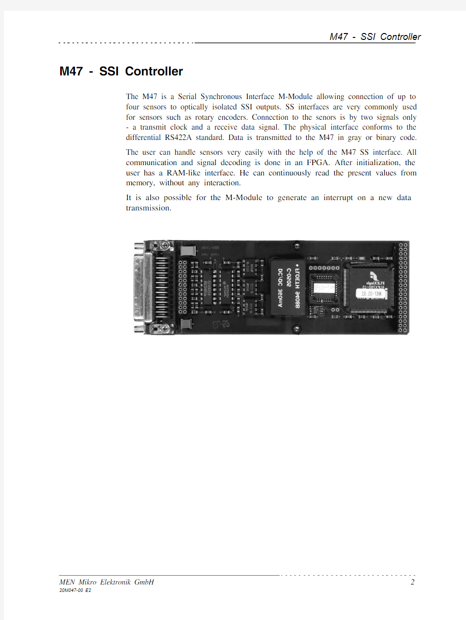
M47 - SSI Controller M47 - SSI Controller
The M47 is a Serial Synchronous Interface M-Module allowing connection of up to
four sensors to optically isolated SSI outputs. SS interfaces are very commonly used
for sensors such as rotary encoders. Connection to the senors is by two signals only
- a transmit clock and a receive data signal. The physical interface conforms to the
differential RS422A standard. Data is transmitted to the M47 in gray or binary code.
The user can handle sensors very easily with the help of the M47 SS interface. All
communication and signal decoding is done in an F PGA. After initialization, the
user has a RAM-like interface. He can continuously read the present values from
memory, without any interaction.
It is also possible for the M-Module to generate an interrupt on a new data
transmission.
Technical Data
SSI Interface:
?4-channel Serial Synchronous Interface (SSI)
?optical isolation for each channel
?RS422A interface
Data Transmission:
?programmable baud rates
?programmable word length (1..32)
Memory:
?16-byte dual-ported RAM
Interfaces:
? 4 RS422 ports, optically isolated
?supply voltage for external sensors etc.: 5V (±10%) @ 200mA max. for all 4
channels
Miscellaneous:
?automatic communication
?RAM-like double buffer user interface
?Gray and binary decoding
?sensor connection detection
?interrupt triggering on a new data transmission
Peripheral Connections:
?via front panel on a shielded 25-pin D-Sub receptacle connector
?via carrier board
M-Module Characteristics:
?A08, D08, INTA, IDENT
Electrical Specifications:
?isolation voltage: 500V DC
?supply voltage/power consumption:
+5V (4.85V..5.25V) @ 500mA typ.
?MTBF: 33,000h @ 50°C
Mechanical Specifications:
?dimensions: conforming to M-Module Standard
?weight: 90g
Environmental Specifications:
?temperature range (operation): 0..+60°C
(industrial temperature range on request)
?temperature range (storage): -40..+85°C
?relative humidity range (operation): max. 95% non-condensing
?relative humidity range (storage): max. 95% non-condensing
?altitude: -300m to + 3,000m
?shock: 15g/0.33ms, 6g/6ms
?vibration: 1g/5..2,000Hz
Safety:
?PCB manufactured with a flammability rating of 94V-0 by UL recognized manu-facturers
EMC:
?tested according to IEC1000-4-2 (ESD) and IEC1000-4-4 (burst) with regard to CE conformity
Software Support:
?MEN Driver Interface System (MDIS)
Block Diagram
Block Diagram
16 Bytes Dual-Ported
RAM (Alternating Buffer)
Opto-coupler
RS422
Opto-coupler RS422
Data Clock
DC
DC
Baud Rate Generator
Time Control M-Module Interface
M-Module ID EEPROM
Control
D0..D7
A1..A7
Serial to Parallel
Gray to Binary
Ordering Information
Ordering Information
Standard Hardware
Accessories
Standard Software
User Manuals
04M047-00M47 hardware
05M000-00M-Module cable, 2m, with 25-pin D-Sub plug/housing to pig tail 05M000-1725 mounting screw sets to fix M-Modules on carrier boards 13M047-06low-level driver sources (MDIS 4), incl. M47 MDIS user manual For use of MDIS you also need MEN ’s basic operating-system specific software package:
13M000-0613M000-0713M000-08MDIS 4 for WindowsNT MDIS 4 for VxWorks MDIS 4 for OS-9
All three include a comprehensive MDIS user guide.20M047-00M47 user manual
About the Manual
This user manual describes the hardware functions of the M-Module, connection of peripheral devices and integration into a system. It also provides additional information for special applications and configurations of the board.
The manual does not include detailed information on individual components (data sheets etc.). A list of literature is given in the appendix.
History
Conventions
This sign marks important notes or warnings concerning proper functionality of the product described in this manual. You should read them in any case.Folder and file names are printed in italics .Bold type is used for emphasis.Hyperlinks are printed in blue color .
Hexadecimal numbers are preceded by "0x", which is the usual C-language convention, and are printed in a monospace type, e.g. 0x00FFFF .
Signal names preceded by a slash ("/") indicate that this signal is either active low or that it becomes active at a falling edge.
Signal directions in signal mnemonics tables generally refer to the corresponding board or component, "in" meaning "to the board or component", "out" meaning "coming from it".
Vertical lines on the outer margin signal technical changes to the previous edition of the manual.
Edition Description Technical Content Date of Issue E1First edition Manfred Schmitz April 4, 1995E2
Second edition
Manfred Schmitz
November 20, 1999
!
italics bold hyperlink 0xFF
/IRQ
in/out
MEN reserves the right to make changes without further notice to any products herein. MEN makes no warranty, representation or guarantee regarding the suitability of its products for any particular purpose, nor does MEN assume any liability arising out of the application or use of any product or circuit, and specifically disclaims any and all liability, including without limitation consequential or incidental damages. "Typical" parameters can and do vary in different applications. All operating parameters, including "Typicals" must be validated for each customer application by customer's technical experts.
MEN does not convey any license under its patent rights nor the rights of others.
MEN products are not designed, intended, or authorized for use as components in systems intended for surgical implant into the body, or other applications intended to support or sustain life, or for any other application in which the failure of the MEN product could create a situation where personal injury or death may occur. Should Buyer purchase or use MEN products for any such unintended or unauthorized application, Buyer shall indemnify and hold MEN and its officers, employees, subsidiaries, affiliates, and distributors harmless against all claims, costs, damages, and expenses, and reasonable attorney fees arising out of, directly or indirectly, any claim of personal injury or death associated with such unintended or unauthorized use, even if such claim alleges that MEN was negligent regarding the design or manufacture of the part.
All brand or product names are trademarks or registered trademarks of their respective holders.
Information in this document has been carefully checked and is believed to be accurate as of the date of publication; however, no responsibility is assumed for inaccuracies. MEN will not be liable for any consequential or incidental damages arising from reliance on the accuracy of this document. The information contained herein is subject to change without notice.
Copyright ? 1999 MEN Mikro Elektronik GmbH. All rights reserved.
Contents Contents
1Getting Started . . . . . . . . . . . . . . . . . . . . . . . . . . . . . . . . . . . . . . . . . . . . . . . . 10
1.1Installation Check List. . . . . . . . . . . . . . . . . . . . . . . . . . . . . . . . . . . . . 10
1.2Installing Driver Software. . . . . . . . . . . . . . . . . . . . . . . . . . . . . . . . . . 10
1.3Power Supply. . . . . . . . . . . . . . . . . . . . . . . . . . . . . . . . . . . . . . . . . . . . 10
2Connection of the M-Module. . . . . . . . . . . . . . . . . . . . . . . . . . . . . . . . . . . . . 11
2.1Peripheral Interfaces . . . . . . . . . . . . . . . . . . . . . . . . . . . . . . . . . . . . . . 11
2.2Host Interface . . . . . . . . . . . . . . . . . . . . . . . . . . . . . . . . . . . . . . . . . . . 13
3Address Organization. . . . . . . . . . . . . . . . . . . . . . . . . . . . . . . . . . . . . . . . . . . 14
4Functional Description. . . . . . . . . . . . . . . . . . . . . . . . . . . . . . . . . . . . . . . . . . 15
4.1SSI Transmission. . . . . . . . . . . . . . . . . . . . . . . . . . . . . . . . . . . . . . . . . 15
4.2Setting the Baud Rate and Bit Width. . . . . . . . . . . . . . . . . . . . . . . . . . 16
4.3Setting the Data Transmission Mode. . . . . . . . . . . . . . . . . . . . . . . . . . 16
4.4Detecting Sensors . . . . . . . . . . . . . . . . . . . . . . . . . . . . . . . . . . . . . . . . 17
4.5Reading Values from the Data RAM. . . . . . . . . . . . . . . . . . . . . . . . . . 17
4.6Interrupts . . . . . . . . . . . . . . . . . . . . . . . . . . . . . . . . . . . . . . . . . . . . . . . 18
4.7M-Module Identification and FLEXlogic . . . . . . . . . . . . . . . . . . . . . . 19
5Appendix . . . . . . . . . . . . . . . . . . . . . . . . . . . . . . . . . . . . . . . . . . . . . . . . . . . . . 20
5.1Literature. . . . . . . . . . . . . . . . . . . . . . . . . . . . . . . . . . . . . . . . . . . . . . . 20
5.2Board Revisions. . . . . . . . . . . . . . . . . . . . . . . . . . . . . . . . . . . . . . . . . . 20
5.3Configuration Plan. . . . . . . . . . . . . . . . . . . . . . . . . . . . . . . . . . . . . . . . 20
Figures
Figure 1:Serial Synchronous Data Transmission . . . . . . . . . . . . . . . . 15
Figure 2:Sequence for Reading Values from the Data RAM . . . . . . . 17
Figure 3:Configuration Plan of M47 Rev. 01 . . . . . . . . . . . . . . . . . . . 20 Tables
Table 1:Pin Assignment of the female 25-Pin D-Sub Connector . . . 11
Table 2:Female 24-Pin Connector . . . . . . . . . . . . . . . . . . . . . . . . . . . 12
Table 3:Signal Correspondence between 24-Pin Module and 96-pin
Carrier Board Connector. . . . . . . . . . . . . . . . . . . . . . . . . . . . 12
Table 4:Signal Mnemonics. . . . . . . . . . . . . . . . . . . . . . . . . . . . . . . . . 12
Table 5:Supported Pins of male 60-Pin Connector on Carrier Board 13
Table 6:Address Map. . . . . . . . . . . . . . . . . . . . . . . . . . . . . . . . . . . . . 14
Table 7:Table of Hardware Revisions . . . . . . . . . . . . . . . . . . . . . . . . 20
Getting Started 1Getting Started
This chapter will give some hints for first installation in a system as a "check list".
1.1Installation Check List
You can use the following "check list" to install the M-Module on a carrier board for
the first time and to test proper functioning of the board.
The M-Module is completely trimmed on delivery. Perform the following procedure !
without the M-Module installed!
;Power-down the system.
;Install the M-Module carrier board in your system without the M-Module.
;Power-up the system.
;Test the carrier board.
;If O.K., power-down the system and remove the carrier board.
;Install the M-Module in slot 0 of the carrier board.
;Initially, do not change any jumpers or switches.
;Insert the carrier board into the system again.
;Power-up the system.
;Load a suitable debugger.
;Access the base address as set, reading word by word.
;If a bus error is occurring now, the M-Module is not plugged properly.
;Write the word 0x0000 to the base address plus 0x0080.
;Write the word 0x0055 to the base address plus 0x0000.
;You should be able to reread these values.
1.2Installing Driver Software
For a detailed description on how to install and use driver software please refer to
the M-Module’s software user manual. F or available software please refer to
Chapter Ordering Information on page 6 or MEN’s website: http://www.men.de.
1.3Power Supply
Power supply to the logic part is done via the carrier board. The necessary voltage is
+5V. The isolated supply voltages (5V) are generated on the M-Module itself.
External sensors can also be supplied by the isolated 5V. External power
consumption should not exceed 1W.
2Connection of the M-Module
2.1
Peripheral Interfaces
There are two possibilities for connecting peripherals:?connection via 25-pin D-Sub connector or ?connection via the carrier board.
When a carrier board with a 96-pin DIN 41612 PCB connection is used for peripheral signals (for example a 6U VMEbus board), these are fed to the M-Module through the 24-pin receptacle connector. You can connect up to four 21-pin connectors to the 96-pin connector (cf. carrier board manual). When these connectors are used, for each M-Module three pins of the DIN 41612 PCB connector cannot be used. The pin numbers for the 96-pin connector shown below are valid for M-Module slot number 3. If other M-Module slots (2, 1 or 0) are used,the value 8, 16 or 24 must be added as appropriate.
Note:The four channels are marked through different colors in the tables.Table 1:
Pin Assignment of the 25-Pin D-Sub Receptacle Connector
Connector types:
?according to DIN41652/MIL-C-24308, with thread bolt UNC 4-40
?mating connector:
25-pin D-Sub plug according to DIN41652/MIL-C-24308, available for ribbon cable (insulation piercing connection), hand-soldering connection or crimp connection
1ACLK+14ADAT A+2ACLK-15ADATA-3
VCC_DC 16GND_DC 4BCLK+17BDAT A+5BCLK-18BDATA-6VCC_DC 19GND_DC 7CCLK+20CDATA+8CCLK-21CDA TA-9
VCC_DC 22GND_DC 10DCLK+23DDATA+11DCLK-24DDA TA-12VCC_DC 25
GND_DC
13
GND_DC
1
14
13
25
Table 2:
24-Pin Receptacle Connector
Connector types:
?two 12-pin receptacles, high-precision, 2.54mm pitch, for square pins ?0.635mm gold, 6.9mm height
?mating connector:
two 12-pin plugs, 2.54mm pitch, square pins ?0.635mm gold Table 3:
Signal Correspondence between 24-Pin Module and 96-pin Carrier Board Connector
Table 4:Signal Mnemonics
23
GND_DC 24GND_DC 21GND_DC 22GND_DC 19GND_DC 20GND_DC 17GND_DC 18GND_DC 15DDA T A+16DDA TA-13DCLK+14DCLK-11CDA T A+12CDA TA-9CCLK+10CCLK-7BDA T A+8BDA TA-5
BCLK+6BCLK-3ADA T A+4ADA TA-1
ACLK+
2
ACLK-
A
B
C
1
ACLK+ACLK-ADA TA+2ADA TA-BCLK+BCLK-3BDA TA+BDA TA-CCLK+4CCLK-CDA T A+CDA T A-5DCLK+DCLK-
DDA TA+
6
DDA TA-
GND_DC GND_DC
7GND_DC GND_DC GND_DC 8GND_DC GND_DC GND_DC
Signal
Direction Function
x CLK+/x CLK-out differential pairs of clock output lines for channels A..D
x DA TA+/x DATA-in differential pairs of data input lines for channels A..D
GND_DC -digital ground reference for channels A..D VCC_DC
-+5V supply voltage for channels A..D (for external sensors). The wattage must not exceed 1W for all channels!
23
12
24
1
A B C
2.2
Host Interface
The M-Module supports the following signals of a 60-pin carrier board interface plug connector:
Note:Only two rows - A and B - of the 60-pin connector are mounted on the M47!Table 5:
Supported Pins of 60-Pin Plug Connector on Carrier Board
Connector types:
?three 20-pin receptacles, high-precision, 2.54mm pitch, for square pins ?0.635mm gold, 6.9mm height
?mating connector:
three 20-pin plugs, 2.54mm pitch, square pins ?0.635mm gold
A
B C 1/CS GND -2
A01+5V -3A02--4A03--5A04--6A05--7A06--8A07--9-D00-10-D01-11-D02-12-D03-13-D04-14-D05-15-D06-16-D07-17---18/DTACK /WRITE -19
-
/IRQ
-20/RESET SYSCLK
-
1
20
A B C
Address Organization
3Address Organization
When using the driver software supplied, you do not need to be familiar with the hardware of the M-Module in detail. However, familiarity with the address organization of the board is essential if you wish to write your own software for the M-Module or do low-level development.
The 256-byte I/O area of the M-Module is hardware-mapped. The address at which individual functions can be addressed from the carrier board is computed from the base address of the M-Module plus the address in the following table.Table 6:
Address Map
Address D15..D8D7..D0
Read Access Write Access 0x00-data d31..d24
C h a n n e l A buffer RAM #10x02-data d23..d16buffer RAM #10x04-data d15..d8buffer RAM #10x06-data d7..d0buffer RAM #10x08-data d31..d24C h a n n e l B buffer RAM #10x0A -data d23..d16buffer RAM #10x0C -data d15..d8buffer RAM #10x0E -data d7..d0buffer RAM #10x10-data d31..d24C h a n n e l C buffer RAM #10x12-data d23..d16buffer RAM #10x14-data d15..d8buffer RAM #10x16-data d7..d0buffer RAM #10x18-data d31..d24C h a n n e l D
buffer RAM #10x1A -data d23..d16buffer RAM #10x1C -data d15..d8buffer RAM #10x1E -data d7..d0buffer RAM #10x21, 0x23..0x3E -
reserved buffer RAM #2
0x80-Control Register
0x84-Mode/PLD Revision Register 0xA0-Status Register
reserved
0xFE
-FLEXlogic/M-Module Identification Register and Interrupt Enable Register
4Functional Description
4.1
SSI Transmission
Serial synchronous interfaces consist of a transmit clock line and a receive data line.When there is no transmission, the clock and data lines are "high". The M-Module transmits a clock sequence to the encoder to obtain the current position value. On the first falling edge of the clock the value is latched at the sensor output. On each of the subsequent rising edges, one bit of data is transmitted to the M-Module. After transmission of a complete data word, the clock line will remain "high" until new data is available at the sensor output.
Figure 1:Serial Synchronous Data Transmission
Data transmission is completely independent, without any interaction of the CPU. If incoming data is Gray encoded, it will be automatically converted to binary code.All four channels are loaded simultaneously.
The bit sequence is written directly to the buffer RAM at the correct bit position. A double buffer mechanism makes sure that a complete data word is read. The CPU always reads a complete data word from one half of the buffer. In the meantime the transmission process uses the other half of the RAM. When the CPU is reading a data word, automatic switching between the two buffer halves is suspended until the complete word has been read. The CPU can easily read current information from the sensor without software overhead.
Clock Data
Transmission Start
Break
Transmission Start
4.2Setting the Baud Rate and Bit Width
An 8-bit control register defines the baud rate and the number of bits in a data word (bit width). The value is equal for all four channels. Setting the number of bits in a data word to zero stops the transmission. The maximum data word length is 32. In applications with different kinds of sensors connected to a single M-Module it might be possible to select the maximum number of bits (32) and adapt the incoming bits by software.
The baud rate must be as slow as the slowest connected sensor.
Control Register (0x80) (read/write)
15..87..2 1..0
-BW BR BW:number of bits in a data word (bit width), 1..32
0 0 0 0 0 0 = stop transmission
0 0 0 0 0 1 = 1 bit in data word
..
1 0 0 0 0 0 = 3
2 bits in data word
Other values are not permitted!
BR:0 0 = 500 kbaud
0 1 = 250 kbaud
1 0 = 125 kbaud
1 1 = 62.5 kbaud
4.3Setting the Data Transmission Mode
The M47 supports both Gray and binary encoded data. You can set the mode in the Mode/PLD Revision Register:
Mode/PLD Revision Register (0x84) (read/write)
15..87 6..4 3..0
-MODE-PLD_Rev MODE:changes between Gray and binary mode.
The setting takes effect on all channels.
0 = Gray encoder (default)
1 = binary encoder
PLD_Rev: PLD revision number (read-only!)
4.4Detecting Sensors
The user can read a 4-bit status register to detect if there is a sensor connected to a channel or not. If the channel bit is '1', the sensor is transferring data to the corresponding channel. The only possibility to clear a bit is to write '0'. After clearing the bits, you must wait for at least two transmission cycles. Then you can read the register again to detect whether a sensor is connected.
Status Register (0xA0) (read)
15..87..43210
-RES TD TC TB TA
RES:reserved (undefined on reading)
TD:0 = clear this bit
1 = channel D is transferring data
TC:0 = clear this bit
1 = channel C is transferring data
TB:0 = clear this bit
1 = channel B is transferring data
TA:0 = clear this bit
1 = channel A is transferring data
4.5Reading Values from the Data RAM
After setting the control register, you should clear the complete data RAM and -after at least one transmission cycle - you must perform a dummy read. Then you can read the current values without any interaction.
Because of the buffer mechanism all four bytes of a channel should be read, even if the data word is smaller. When reading a value, you must stick to the following order to get valid data:
Figure 2:Sequence for Reading Values from the Data RAM
Read Data Byte
d31..d24
Read Data Byte
d23..d16
Read Data Byte
d15..d8
Read Data Byte
d7..d0
4.6
Interrupts
For special requirements the M47 M-Module can trigger an interrupt to the carrier board. Interrupts to the M-Module are in accordance with type a) of the M-Module Specification (see Chapter 5.1 Literature on page 20), i.e., the interrupt request is reset by software, but the M47 M-Module itself is not able to supply a vector during the interrupt-acknowledge cycle.
The interrupt cause is receiving a new data word. It is not possible to mask this interrupt (this should be done on the carrier board). The INT bit in the Interrupt Enable Register can be read and written. Therefore, also if the interrupt function is not used, the user can make a software acknowledge by setting this bit. When the bit is cleared a new value is available.
Interrupt Enable Register (0xFE ) (read/write)
INT:0 = new data available
1 = no new data available
15..87 6..43210-INT
-FLEX TMS
SEL
FLEX/ID CLK
FLEX/ID DA TA
4.7
M-Module Identification and FLEXlogic
The M47 M-Module is supplied with an identification EEPROM in accordance with the M-Module specification.
FLEXlogic/M-Module Identification (0xFE ) (read/write)
Both the FLEXlogic and the M-Module identification EEPROM can be accessed at address 0xFE . The selection is made through bit SEL:
0 = FLEXlogic access
1 = M-Module ID EEPROM access
15..87
6..432
1
-INT
-FLEX
TMS
SEL
FLEX CLK FLEX DA TA
---ID CLK
ID DA TA
Appendix
5Appendix
5.1
Literature
?M-Module Standard:
ANSI/VITA 12-1996, M-Module Specification;VMEbus International Trade Association 7825 E. Gelding Dr., Ste. 104, Scottsdale, AZ 85260
WWW: https://www.doczj.com/doc/8f558936.html,
5.2
Board Revisions
Table 7:
Table of Hardware Revisions
Note:As of hardware revision 01.04 the M47 M-Module also supports binary
encoders in addition to Gray encoders.
5.3Configuration Plan
Figure 3:Configuration Plan of M47 Rev. 01
Revision
Comment
Restrictions
00.xx first revision released M-Module identification not implemented yet 01.xx
second revision released
none known