
1 MHz to 10 GHz, 50 dB
Dual Log Detector/Controller Preliminary Technical Data ADL5519
Rev. PrB
Information furnished by Analog Devices is believed to be accurate and reliable. However, no
responsibility is assumed by Analog Devices for its use, nor for any infringements of patents or other rights of third parties that may result from its use. Specifications subject to change without notice. No license is granted by implication or otherwise under any patent or patent rights of Analog Devices. T rademarks and registered trademarks are the property of their respective owners. One Technology Way, P.O. Box 9106, N orwood, MA 02062-9106, U.S.A. Tel: 781.329.4700 https://www.doczj.com/doc/7717600398.html, Fax: 781.461.3113 ?2006 Analog Devices, Inc. All rights reserved.
FEATURES
Wide bandwidth: 1 MHz to 10 GHz
Dual-channel and channel difference outputs ports Integrated accurately scaled temperature sensor
50 dB dynamic range up to 8 GHz
Stability over temperature ±0.5 dB
Low noise measurement/controller output VOUT
Pulse response time: 8/10 ns (fall/rise)
Small footprint 5 mm x 5 mm LFCSP package
Supply operation: 3.0 V to 5.5 V @ 65 mA
Fabricated using high speed SiGe process
APPLICATIONS
RF transmitter PA setpoint control and level monitoring Power monitoring in radiolink transmitters
RSSI measurement in base stations, WLAN, WiMAX, radar Antenna VSWR monitor
Dual-channel wireless infrastructure radios
GENERAL DESCRIPTION
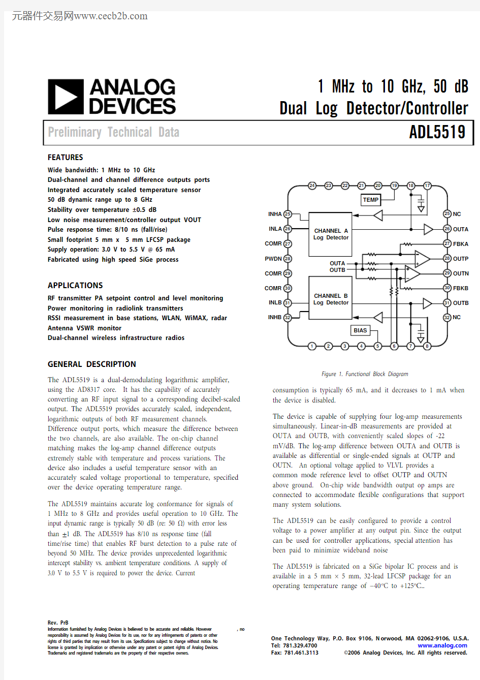
The ADL5519 is a dual-demodulating logarithmic amplifier,
using the AD8317 core. It has the capability of accurately converting an RF input signal to a corresponding decibel-scaled output. The ADL5519 provides accurately scaled, independent, logarithmic outputs of both RF measurement channels. Difference output ports, which measure the difference between the two channels, are also available. The on-chip channel matching makes the log-amp channel difference outputs extremely stable with temperature and process variations. The device also includes a useful temperature sensor with an accurately scaled voltage proportional to temperature, specified over the device operating temperature range.
The ADL5519 maintains accurate log conformance for signals of 1 MHz to 8 GHz and provides useful operation to 10 GHz. The input dynamic range is typically 50 dB (re: 50 Ω) with error less than ±1 dB. The ADL5519 has 8/10 ns response time (fall
time/rise time) that enables RF burst detection to a pulse rate of beyond 50 MHz. The device provides unprecedented logarithmic intercept stability vs. ambient temperature conditions. A supply of 3.0 V to 5.5 V is required to power the device. Current
consumption is typically 65 mA, and it decreases to 1 mA when the device is disabled.
The device is capable of supplying four log-amp measurements simultaneously. Linear-in-dB measurements are provided at OUTA and OUTB, with conveniently scaled slopes of -22
mV/dB. The log-amp difference between OUTA and OUTB is available as differential or single-ended signals at OUTP and OUTN. An optional voltage applied to VLVL provides a common mode reference level to offset OUTP and OUTN above ground. On-chip wide bandwidth output op amps are connected to accommodate flexible configurations that support many system solutions.
The ADL5519 can be easily configured to provide a control voltage to a power amplifier at any output pin. Since the output can be used for controller applications, special attention has been paid to minimize wideband noise
The ADL5519 is fabricated on a SiGe bipolar IC process and is available in a 5 mm × 5 mm, 32-lead LFCSP package for an operating temperature range of ?40o C to +125o C..
C
L
P
B
V
L
V
L
V
R
E
F
A
D
J
B
V
P
S
B
C
L
P
A
T
E
M
P
V
P
S
R
A
D
J
A
V
S
T
A
V
S
T
V
P
S
A
COMR
O
M
R
O
M
R
C
O
M
R
C
O
M
R
Figure 1. Functional Block Diagram
ADL5519
Preliminary Technical Data
Rev. PrB | Page 2 of 27
TABLE OF CONTENTS
Features..............................................................................................1 Applications.......................................................................................1 General Description.........................................................................1 Specifications.....................................................................................3 Absolute Maximum Ratings............................................................9 ESD Caution..................................................................................9 Pin Configuration and Function Descriptions...........................10 Typical Performance Characteristics...........................................12 Theory of Operation......................................................................13 Using the ADL5519........................................................................14 Basic Connections......................................................................14 Input Signal Coupling................................................................14 Temperature Sensor Interface...................................................14 Power-Down Interface...............................................................15 Setpoint Interface, VST[A, B]...................................................15 Output Interface, OUT[A, B]...................................................15 Difference Output, OUT[P , N].................................................15 Measurement Mode...................................................................16 Controller Mode.........................................................................17 Temperature Compensation Adjustment................................20 Device Calibration and Error Calculation..............................20 Altering the Slope.......................................................................21 Output Filtering..........................................................................21 Basis for Error Calculations......................................................21 Evaluation Board............................................................................23 Outline Dimensions.......................................................................27 Ordering Guide.. (27)
Preliminary Technical Data
ADL5519
Rev. PrB | Page 3 of 27
SPECIFICATIONS
V POS = 5 V , C LPF = 1000 pF, T A = 25°C, 52.3 Ω termination resistor at INHI, unless otherwise noted. Table 1.
Parameter
Conditions
Min Typ Max Unit SIGNAL INPUT INTERFACE INH[A, B] (Pins 19. 24)
Specified Frequency Range 0.001
10 GHz DC Common-Mode Voltage
V POS – 0.6 V MEASUREMENT MODE
OUT[A, B] (Pins 12, 7) shorted to VST[A,B] (Pin 13, 6), OUT[P , N] (Pins 10, 9) shorted to FBK[A, B] [Pins 11, 8] respectively, sinusoidal input signal, error referred to best fit line using linear regression @ P INH[A, B] = ?40 dBm and ?20 dBm, T A = +25°C
f = 100 MHz ADJA = ADJB = TBD to GND
Input Impedance
TBD
Ω||pF
OUT[A, B] ±1 dB Dynamic Range T A = +25°C 50 dB ?40°C < T A < +85°C 46 dB
?40°C < T A < +125°C TBD dB
OUT[A, B] Maximum Input Level ±1 dB error ?3 dBm OUT[A, B] Minimum Input Level ±1 dB error ?53 dBm
OUT[A, B, P , N] Slope TBD ?22 TBD mV/dB OUT[A, B] Intercept
TBD 15 TBD dBm Output Voltage - High Power In Pins OUT[A, B] @ P INH[A, B] = ?10 dBm TBD 0.58 TBD V Output Voltage - Low Power In Pins OUT[A, B] @ P INH[A, B] = ?40 dBm TBD 1.27 TBD V Temperature Sensitivity
Deviation from OUT[A, B] @ 25°C
?40°C < T A < 85°C; P INH[A, B] = ?10 dBm TBD dB ?40°C < T A < 85°C; P INH[A, B] = ?25 dBm TBD dB ?40°C < T A < 85°C; P INH[A, B] = ?40 dBm TBD dB OUTP-OUTN Dynamic Gain Range ±1 dB error
TBD dB
?40°C < T A < 85°C
TBD dB Temperature Sensitivity
OUTP-OUTN Dynamic Gain Range
TBD ?40°C < T A < 85°C; P INH[A, B] = ?10 dBm, ?25 dBm TBD dB ?40°C < T A < 85°C; P INH[A, B] = ?25 dBm, ?25 dBm TBD dB ?40°C < T A < 85°C; P INH[A, B] = ?40 dBm, ?25 dBm TBD dB Input A to Input B Isolation
TBD dB Input A to OUTB Isolation Freq separation = 1 kHz
TBD Input B to OUTA Isolation P INHB = ?50 dBm, OUTB = OUTB PINHB ± 1 dB TBD dB
P INHA = ?50 dBm, OUTA = OUTA PINHA ± 1 dB
TBD
dB
f = 900 MHz
ADJA = ADJB = TBD to GND Input Impedance
TBD Ω||pF
OUT[A, B] ±1 dB Dynamic Range T A = +25°C
50 dB ?40°C < T A < +85°C 46 dB
?40°C < T A < +125°C TBD OUT[A, B] Maximum Input Level ±1 dB error ?3 dBm OUT[A, B] Minimum Input Level ±1 dB error ?53 dBm OUT[A, B, P , N] Slope TBD ?22 TBD mV/dB OUT[A, B] Intercept
TBD 15 TBD dBm Output Voltage - High Power In Pins OUT[A, B] @ P INH[A, B] = ?10 dBm TBD 0.58 TBD V Output Voltage - Low Power In
Pins OUT[A, B] @ P INH[A, B] = ?40 dBm
TBD 1.27 TBD V
ADL5519
Preliminary Technical Data
Rev. PrB | Page 4 of 27
Parameter
Conditions
Min
Typ
Max
Unit
Temperature Sensitivity Deviation from OUT[A, B] @ 25°C
25°C < T A < 85°C; P INH[A, B] = ?10 to -15 dBm ±.25 TBD dB -20°C < T A <25°C; P INH[A, B] = ?10 to -15 dBm ±.25 TBD dB 25°C < T A < 85°C; P INH[A, B] = ?10 to -40 dBm ±.25 TBD dB -20°C < T A <25°C; P INH[A, B] = ?10 to -40 dBm ±.5 TBD
dB
OUTP-OUTN Dynamic Gain Range ±1 dB error
TBD dB ?40°C < T A < 85°C TBD dB Temperature Sensitivity OUTP-OUTN Dynamic Gain Range
TBD 25°C < T A < 85°C; P INH[A, B] = ?10 to -15 dBm ±.25 TBD dB -20°C < T A <25°C; P INH[A, B] = ?10 to -15 dBm ±.25 TBD dB 25°C < T A < 85°C; P INH[A, B] = ?10 to -40 dBm ±.25 TBD dB -20°C < T A <25°C; P INH[A, B] = ?10 to -40 dBm ±.5 TBD dB Input A to Input B Isolation TBD dB Input A to OUTB Isolation Freq separation = 1 kHz TBD Input B to OUTA Isolation P INHB = ?50 dBm, OUTB = OUTB PINHB ± 1 dB TBD dB P INHA = ?50 dBm, OUTA = OUTA PINHA ± 1 dB TBD
dB
f = 1.9 GHz
ADJA = ADJB = TBD to GND Input Impedance
950||0.38 Ω||pF
OUT[A, B] ±1 dB Dynamic Range T A = +25°C 50 dB ?40°C < T A < +85°C 48 dB ?40°C < T A < +125°C TBD OUT[A, B] Maximum Input Level ±1 dB error ?4 dBm OUT[A, B] Minimum Input Level ±1 dB error ?54 dBm OUT[A, B, P , N] Slope TBD ?22 TBD mV/dB OUT[A, B] Intercept TBD 14 TBD dBm Output Voltage - High Power In Pins OUT[A, B] @ P INH[A, B] = ?10 dBm TBD 0.54 TBD V Output Voltage - Low Power In Pins OUT[A, B] @ P INH[A, B] = ?40 dBm TBD 1.21 TBD V Temperature Sensitivity Deviation from OUT[A, B] @ 25°C
25°C < T A < 85°C; P INH[A, B] = ?10 to -15 dBm ±.25 TBD dB -20°C < T A <25°C; P INH[A, B] = ?10 to -15 dBm ±.25 TBD dB 25°C < T A < 85°C; P INH[A, B] = ?10 to -40 dBm ±.25 TBD dB -20°C < T A <25°C; P INH[A, B] = ?10 to -40 dBm ±.5 TBD dB
OUTP-OUTN Dynamic Gain Range ±1 dB error
TBD dB ?40°C < T A < 85°C TBD dB Temperature Sensitivity OUTP-OUTN Dynamic Gain Range
TBD 25°C < T A < 85°C; P INH[A, B] = ?10 to -15 dBm ±.25 TBD dB -20°C < T A <25°C; P INH[A, B] = ?10 to -15 dBm ±.25 TBD dB 25°C < T A < 85°C; P INH[A, B] = ?10 to -40 dBm ±.25 TBD dB -20°C < T A <25°C; P INH[A, B] = ?10 to -40 dBm ±.5 TBD dB Input A to Input B Isolation TBD dB Input A to OUTB Isolation Freq separation = 1 kHz TBD Input B to OUTA Isolation P INHB = ?50 dBm, OUTB = OUTB PINHB ± 1 dB TBD dB P INHA = ?50 dBm, OUTA = OUTA PINHA ± 1 dB TBD dB f = 2.2 GHz
ADJA = ADJB = TBD to GND Input Impedance
TBD
Ω||pF
OUT[A, B] ±1 dB Dynamic Range T A = +25°C
50 dB ?40°C < T A < +85°C 47 dB
?40°C < T A < +125°C
TBD
Preliminary Technical Data
ADL5519
Rev. PrB | Page 5 of 27
Parameter Conditions
Min
Typ
Max
Unit
OUT[A, B] Maximum Input Level ±1 dB error
?5 dBm OUT[A, B] Minimum Input Level ±1 dB error ?55 dBm OUT[A, B, P , N] Slope ?22 mV/dB OUT[A, B] Intercept 14 dBm Output Voltage - High Power In Pins OUT[A, B] @ P INH[A, B] = ?10 dBm 0.53 V Output Voltage - Low Power In Pins OUT[A, B] @ P INH[A, B] = ?40 dBm 1.20 V Temperature Sensitivity Deviation from OUT[A, B] @ 25°C
25°C < T A < 85°C; P INH[A, B] = ?10 to -15 dBm ±.25 TBD dB -20°C < T A <25°C; P INH[A, B] = ?10 to -15 dBm ±.25 TBD dB 25°C < T A < 85°C; P INH[A, B] = ?10 to -40 dBm ±.25 TBD dB -20°C < T A <25°C; P INH[A, B] = ?10 to -40 dBm ±.5 TBD
dB
OUTP-OUTN Dynamic Gain Range ±1 dB error
TBD dB ?40°C < T A < 85°C TBD dB Temperature Sensitivity OUTP-OUTN Dynamic Gain Range
TBD 25°C < T A < 85°C; P INH[A, B] = ?10 to -15 dBm ±.25 TBD dB -20°C < T A <25°C; P INH[A, B] = ?10 to -15 dBm ±.25 TBD dB 25°C < T A < 85°C; P INH[A, B] = ?10 to -40 dBm ±.25 TBD dB -20°C < T A <25°C; P INH[A, B] = ?10 to -40 dBm ±.5 TBD dB Input A to Input B Isolation TBD dB Input A to OUTB Isolation Freq separation = 1 kHz TBD Input B to OUTA Isolation 1P INHB = ?50 dBm, OUTB = OUTB PINHB ± 1 dB TBD dB P INHA = ?50 dBm, OUTA = OUTA PINHA ± 1 dB TBD dB
f = 3.6 GHz
ADJA = ADJB = TBD to GND
Input Impedance
TBD
Ω||pF
OUT[A, B] ±1 dB Dynamic Range T A = +25°C
42 dB ?40°C < T A < +85°C 40 dB ?40°C < T A < +125°C TBD OUT[A, B] Maximum Input Level ±1 dB error ?6 dBm OUT[A, B] Minimum Input Level ±1 dB error ?48 dBm OUT[A, B, P , N] Slope ?22 mV/dB OUT[A, B] Intercept 11 dBm Output Voltage - High Power In Pins OUT[A, B] @ P INH[A, B] = ?10 dBm 0.47 V Output Voltage - Low Power In Pins OUT[A, B] @ P INH[A, B] = ?40 dBm 1.16 V Temperature Sensitivity Deviation from OUT[A, B] @ 25°C
?40°C < T A < 85°C; P INH[A, B] = ?10 dBm
TBD dB ?40°C < T A < 85°C; P INH[A, B] = ?25 dBm
TBD dB ?40°C < T A < 85°C; P INH[A, B] = ?40 dBm TBD
dB
OUTP-OUTN Dynamic Gain Range ±1 dB error
TBD dB ?40°C < T A < 85°C TBD dB Temperature Sensitivity OUTP-OUTN Dynamic Gain Range
TBD ?40°C < T A < 85°C; P INH[A, B] = ?10 dBm, ?25 dBm TBD dB ?40°C < T A < 85°C; P INH[A, B] = ?25 dBm, ?25 dBm TBD dB ?40°C < T A < 85°C; P INH[A, B] = ?40 dBm, ?25 dBm TBD dB Input A to Input B Isolation TBD dB Input A to OUTB Isolation Freq separation = 1 kHz TBD Input B to OUTA Isolation 2P INHB = ?50 dBm, OUTB = OUTB PINHB ± 1 dB TBD dB P INHA = ?50 dBm, OUTA = OUTA PINHA ± 1 dB TBD dB
ADL5519
Preliminary Technical Data
Rev. PrB | Page 6 of 27
Parameter Conditions
Min
Typ
Max
Unit
f = 5.8 GHz
ADJA = ADJB = TBD to GND
Input Impedance
TBD
Ω||pF
OUT[A, B] ±1 dB Dynamic Range T A = +25°C 50 dB ?40°C < T A < +85°C 48 dB ?40°C < T A < +125°C TBD OUT[A, B] Maximum Input Level ±1 dB error ?4 dBm OUT[A, B] Minimum Input Level ±1 dB error ?54 dBm OUT[A, B, P , N] Slope ?22 mV/dB OUT[A, B] Intercept 16 dBm Output Voltage - High Power In Pins OUT[A, B] @ P INH[A, B] = ?10 dBm 0.59 V Output Voltage - Low Power In Pins OUT[A, B] @ P INH[A, B] = ?40 dBm 1.27 V Temperature Sensitivity Deviation from OUT[A, B] @ 25°C
?40°C < T A < 85°C; P INH[A, B] = ?10 dBm
TBD dB ?40°C < T A < 85°C; P INH[A, B] = ?25 dBm
TBD dB ?40°C < T A < 85°C; P INH[A, B] = ?40 dBm TBD
dB
OUTP-OUTN Dynamic Gain Range ±1 dB error
TBD dB ?40°C < T A < 85°C TBD dB Temperature Sensitivity OUTP-OUTN Dynamic Gain Range
TBD ?40°C < T A < 85°C; P INH[A, B] = ?10 dBm, ?25 dBm TBD dB ?40°C < T A < 85°C; P INH[A, B] = ?25 dBm, ?25 dBm TBD dB ?40°C < T A < 85°C; P INH[A, B] = ?40 dBm, ?25 dBm TBD dB Input A to Input B Isolation TBD dB Input A to OUTB Isolation Freq separation = 1 kHz TBD Input B to OUTA Isolation 3P INHB = ?50 dBm, OUTB = OUTB PINHB ± 1 dB TBD dB P INHA = ?50 dBm, OUTA = OUTA PINHA ± 1 dB TBD dB f = 8 GHz
ADJA = ADJB = TBD to GND Input Impedance
TBD
Ω||pF
OUT[A, B] ±1 dB Dynamic Range T A = +25°C 44 dB ?40°C < T A < +85°C dB ?40°C < T A < +125°C
OUT[A, B] Maximum Input Level ±1 dB error ?2 dBm OUT[A, B] Minimum Input Level ±1 dB error ?46 dBm OUT[A, B, P , N] Slope ?22 mV/dB OUT[A, B] Intercept 21 dBm Output Voltage - High Power In Pins OUT[A, B] @ P INH[A, B] = ?10 dBm 0.7 V Output Voltage - Low Power In Pins OUT[A, B] @ P INH[A, B] = ?40 dBm 1.39 V Temperature Sensitivity Deviation from OUT[A, B] @ 25°C
?40°C < T A < 85°C; P INH[A, B] = ?10 dBm
TBD dB ?40°C < T A < 85°C; P INH[A, B] = ?25 dBm
TBD dB ?40°C < T A < 85°C; P INH[A, B] = ?40 dBm TBD
dB
OUTP-OUTN Dynamic Gain Range ±1 dB error
TBD dB ?40°C < T A < 85°C TBD dB Temperature Sensitivity OUTP-OUTN Dynamic Gain Range
TBD ?40°C < T A < 85°C; P INH[A, B] = ?10 dBm, ?25 dBm TBD dB ?40°C < T A < 85°C; P INH[A, B] = ?25 dBm, ?25 dBm TBD dB ?40°C < T A < 85°C; P INH[A, B] = ?40 dBm, ?25 dBm TBD dB Input A to Input B Isolation TBD dB Input A to OUTB Isolation Freq separation = 1 kHz
TBD
Preliminary Technical Data
ADL5519
Rev. PrB | Page 7 of 27
Parameter
Conditions
Min Typ Max Unit Input B to OUTA Isolation P INHB = ?50 dBm, OUTB = OUTB PINHB ± 1 dB TBD dB
P INHA = ?50 dBm, OUTA = OUTA PINHA ± 1 dB
TBD
dB
OUTPUT INTERFACE
OUT[A, B] (Pins 12, 7), OUT[P , N] (Pins 10, 9)
OUT[A, B] Voltage Range Min VST[A, B] = TBD RFIN = open RL ≥ 240Ω to ground
TBD V
VST[A, B] = 0V RFIN = open RL ≥ 240Ω to ground
TBD V OUT[P , N] output
OUT[A, B] = OUT[P , N] VLVL
OUT[P , N] Voltage Range Min FBK[A, B] = TBD RFIN = open RL ≥ 240Ω to ground
TBD V
FBK[A, B] = 0V RFIN = open RL ≥ 240Ω to ground
TBD V Source/Sink Current Output held at 1V to 1% change 2.2 mA Small Signal Bandwidth RFIN = ?10 dBm, from CLP[A,B] to OUT[A,B] TBD MHz
Output Noise RF Input = 2.2 GHz, –10 dBm, f NOISE = 100 kHz,
C LP[A,B] = open
TBD nV/√Hz Fall Time Input level = no signal to –10 dBm, 90% to 10%,
C LP[A,B] = 8 pF
TBD ns Fall Time Input level = no signal to –10 dBm, 90% to 10%,
C LP[A,B] = open;
TBD ns Rise Time Input level = ?10 dBm to no signal, 10% to 90%,
C LP[A, B] = 8 pF
TBD ns Rise Time
Input level = ?10 dBm to no signal, 10% to 90%,
C LP[A,B] = open,
TBD ns Video Bandwidth (or Envelope Bandwidth)
50 M H z SETPOINT INTERFACE VST[A, B] (Pins 13, 6)
Nominal Input Range Input level = 0 dBm, measurement mode 0.5 V
Input level = –50 dBm, measurement mode 1.75 V Logarithmic Scale Factor ?45 dB/V Logarithmic Intercept
TBD
Input Resistance Input level = ?20 dBm, controller mode, VST[A,B] = 1 V
40 k Ω DIFFERENCE LEVEL ADJUST VLVL (Pin 4)
Voltage Range
OUT[P , N] = FBK[A, B] TBD V OUT[P , N] Voltage Range OUT[P , N] = FBK[A, B] TBD V Input Impedance
TBD Ω||pF TEMPERATURE COMPENSATION ADJ[A, B] (Pins 17, 2)
Input Resistance
ADJ[A, B] = 0.9 V, sourcing 50 μA 13
k Ω Disable Threshold Voltage ADJ[A, B] = open
V POS – 0.4
V
VOLTAGE REFERENCE VREF (Pin 3)
Output Voltage
1.15
V
Temperature Sensitivity ?40°C < T A < +85°C TBD mV/o C Current Limit Source/Sink
3/3 mA TEMPERATURE REFERENCE TEMP (Pin 15) Output Voltage
1.3
V
Temperature Sensitivity ?40°C < T A < +125°C 4.5 mV/o C Current Limit Source/Sink
5/40
mA/uA
POWER-DOWN INTERFACE Pin PWDN
Logic Level to Enable Logic LO enables TBD V Logic Level to Disable Logic HI disables TBD V Input Current Logic HI PWDN = 5 V TBD μA
Logic LO PWDN = 0 V
TBD μA
Enable Time
PWDN LO to OUTA/OUTB at 100% final value, C LPA/B = Open, C HPA/B = 10 nF, RF in = 0 dBm
TBD μs
ADL5519
Preliminary Technical Data
Rev. PrB | Page 8 of 27
Parameter Conditions
Min
Typ
Max
Unit
Disable Time PWDN HI to OUTA/OUTB at 10% final value, C LPA/B = Open, C HPA/B = 10nF, RF in = 0 dBm TBD μs POWER INTERFACE
VPS[A, B, R] (Pins 18, 1, 16) Supply Voltage 3.0 5.5 V Quiescent Current
65 mA
vs. Temperature ?40°C ≤ T A ≤ +125°C
TBD μA/°C Disable Current
ADJ[A,B] = PWDN = VPOS
1 mA
Preliminary Technical Data
ADL5519
Rev. PrB | Page 9 of 27
ABSOLUTE MAXIMUM RATINGS
Table 2.
Parameter Rating Supply Voltage: VPSA, VPSB, VPSR 5.7 V V SET Voltage: VSTA, VSTB 0 to V POS Input Power (Single-Ended, Re: 50 Ω) INHA, INLA, INHB, INLB 12 dBm Internal Power Dissipation θJA
55°C/W Maximum Junction Temperature 165°C
Operating Temperature Range ?40°C to +125°C Storage Temperature Range
?65°C to +150°C Lead Temperature (Soldering 60 sec)
260°C
Stresses above those listed under Absolute Maximum Ratings
may cause permanent damage to the device. This is a stress rating only; functional operation of the device at these or any other conditions above those indicated in the operational
section of this specification is not implied. Exposure to absolute
maximum rating conditions for extended periods may affect device reliability.
ESD CAUTION
ESD (electrostatic discharge) sensitive device. Electrostatic charges as high as 4000 V readily accumulate on the human body and test equipment and can discharge without detection. Although this product features proprietary ESD protection circuitry, permanent damage may occur on devices subjected to high energy electrostatic discharges. Therefore, proper ESD precautions are recommended to avoid performance
degradation or loss of functionality.
ADL5519
Preliminary Technical Data
Rev. PrB | Page 10 of 27
PIN CONFIGURATION AND FUNCTION DESCRIPTIONS
VSTA
CLPA TEMP VPSR ADJA VPSA O U T A F B K A O U T P O U T N F B K B O U T B VSTB CLPB VLVL VREF ADJB VPSB
1COMR 2COMR 345678
2423222120191817910111213141516
3231302928272625
COMR COMR N C N C
I N H B I N L B C O M R P W D N I N L A I N H A
C O M R C O M R
Figure 2. Pin Configuration
Table 3. Pin Function Descriptions
PI N N
ame Description
1 COMR Common for difference output and Temp Sensor
2 COMR Common for difference output and Temp Sensor
3 VPSB
Positive Supply for Channel B. Must be the same as VPS[A/R]. Apply 3.0V to 5.5V supply voltage. 4 ADJB Dual function pin. Channel B Temperature adjust. Connect a resistor to ground to vary temperature compensation. Connect to VPS[A/B/R] to power down Channel B. 5 VREF 1.15V voltage reference
6 VLVL DC common mode adjust for difference output
7 CLPB Loop filter pin for Channel B
8 VSTB
Setpoint Control input for Channel B 9 NC No Connect
10 OUTB Output voltage for Channel B 11 FBKB Difference op-amp feedback pin
12 OUTN Difference output (OUTB - OUTA + VLVL) 13 OUTP Difference output (OUTA - OUTB + VLVL) 14 FBKA Difference op-amp feedback pin 15 OUTA
Output voltage for Channel A 16 NC No Connect
17 VSTA Setpoint Control input for Channel A 18 CLPA Loop filter pin for Channel A
19 TEMP
Temp Sensor output (1.3V with 4.5mV/o C slope)
20 VPSR Positive Supply for difference output and temperature sensor. Must be the same as VPS[A/B]. Apply 3.0V to 5.5V supply voltage.
21 ADJA Dual function pin. Channel A Temperature adjust. Connect a resistor to ground to vary temperature compensation. Connect to VPS[A/B/R] to power down Channel A.
22 VPSA Positive Supply for Channel A. Must be the same as VPS[B/R]. Apply 3.0V to 5.5V supply voltage. 23 COMR Common for difference output and Temp Sensor 24 COMR Common for difference output and Temp Sensor 25 INHA AC coupled RF input for Channel A 26 INLA AC coupled RF common for Channel A
27 COMR Common for difference output and Temp Sensor 28
PWDN
Power down for difference output and Temp Sensor
Preliminary Technical Data
ADL5519
Rev. PrB | Page 11 of 27
29 COMR Common for difference output and Temp Sensor
30 COMR Common for difference output and Temp Sensor 31 INLB AC coupled RF common for Channel B 32 INHB
AC coupled RF input for Channel B Paddle Internally connected to COMR
ADL5519
Preliminary Technical Data
Rev. PrB | Page 12 of 27
TYPICAL PERFORMANCE CHARACTERISTICS
V P = 5 V; T
A = +25°C, –40°C, +85°C; CLPA/
B = OPEN. Colors: +25°
C black, –40°C blue, +85°C red.
Figure 3: OUT[A, B] Voltage and Log Conformance vs. Input Amplitude
at 450 MHz, Typical Device, ADJ[A, B] = 0 V, Sine Wave, Differential
Drive, Figure 4: Distribution of OUT[A, B] Voltage and Error over Temperature After Ambient Normalization vs. Input Amplitude for at Least 30
Devices from Multiple Lots, Frequency = 450 MHz, ADJ[A, B] = 0 V, Sine
Wave, Differential Drive
Figure 5: Distribution of [OUTA – OUTB] Gain vs. Input Amplitude over
Temperature for at Least 30 Devices from Multiple Lots, Frequency =
450 MHz, ADJ[A, B] = 0 V, Sine Wave, Differential Drive
Figure 6: OUT[P, N]Gain and Log Conformance vs. Input Amplitude at 450 MHz, Typical Device, ADJ[A, B] = 0 V, Sine Wave, Differential Drive
(Note that the OUTP and OUTN Error Curves Overlap)
Figure 7: Distribution of [OUTP ? OUTN] Gain and Error over Temperature After Ambient Normalization vs. Input Amplitude for at Least 30 Devices from Multiple Lots, Frequency = 450 MHz, ADJ[A, B] = 0 V, Sine Wave, Differential Drive, P IN Ch. B = ?25 dBm, Channel A
Swept
Figure 8: OUT[A, B] Voltage and Log Conformance vs. Input Amplitude at 880 MHz, Typical Device, ADJ[A, B] = 0.5 V, Sine Wave, Differential
Drive,
Preliminary Technical Data
ADL5519
Rev. PrB | Page 13 of 27
THEORY OF OPERATION
The ADL5519 is a dual-channel 6-stage demodulating
logarithmic amplifier, specifically designed for use in RF measurement and power control applications at frequencies up to 10 GHz. Sharing much of its design with the AD8317 logarithmic detector/controller, the ADL5519 maintains tight intercept variability vs. temperature over a 50 dB range. Each measurement channel offers equivalent performance to the AD8317. The complete circuit block diagram is shown in Figure 9.
C L P V L V V R E A
D J V P S L P A
E M P
P S R
D J A
V S T A
V S T
P S A
COMR O M R
O M R
C O M C O M
Figure 9. Block Diagram
Each measurement channel is a fully differential design and uses a proprietary, high speed SiGe process, extending high frequency performance. Figure 10 shows the basic diagram of the ADL5519’s channel A signal path, the functionality is identical for channel B.
OUTA VSTA
CLPA
I V
Figure 10. Single Channel Block Diagram
The maximum input with ±1 dB log-conformance error is typically 0 dBm (re: 50 Ω). The noise spectral density referred to the input is 1.15 nV/√Hz, which is equivalent to a voltage of 118 μV rms in a 10.5 GHz bandwidth or a noise power of ?66 dBm (re: 50 Ω). This noise spectral density sets the lower limit of the dynamic range. However, the low end accuracy of the ADL5519 is enhanced by specially shaping the demodulating transfer characteristic to partially compensate for errors due to internal noise. The common pin, COMR, provides a quality low impedance connection to the printed circuit board (PCB) ground. The package paddle, which is internally connected to the COMR pin, should also be grounded to the PCB to reduce thermal impedance from the die to the PCB.
The logarithmic function is approximated in a piecewise
fashion by six cascaded gain stages. (For a more comprehensive explanation of the logarithm approximation, please refer to the AD8307 data sheet, available at https://www.doczj.com/doc/7717600398.html,.) The cells have a nominal voltage gain of 9 dB each and a 3 dB bandwidth of 10.5 GHz. Using precision biasing, the gain is stabilized over temperature and supply variations. The overall dc gain is high, due to the cascaded nature of the gain stages. An offset
compensation loop is included to correct for offsets within the cascaded cells. At the output of each of the gain stages, a square-law detector cell is used to rectify the signal.
The RF signal voltages are converted to a fluctuating differential current having an average value that increases with signal level. Along with the six gain stages and detector cells, an additional detector is included at the input of each measurement channel,, providing a 50 dB dynamic range in total. After the detector currents are summed and filtered, the following function is formed at the summing node: I D × log 10(V IN /V INTERCEPT ) where:
I D is the internally set detector current. V IN is the input signal voltage.
V INTERCEPT is the intercept voltage (that is, when V IN = V INTERCEPT , the output voltage would be 0 V , if it were capable of going to 0 V).
ADL5519
Preliminary Technical Data
Rev. PrB | Page 14 of 27
USING THE ADL5519
BASIC CONNECTIONS
The ADL5519 is specified for operation up to 10 GHz; as a result, low impedance supply pins with adequate isolation between functions are essential. A power supply voltage of between 3.0 V and 5.5 V should be applied to VPSA, VPSB, and VPSR. Power supply decoupling capacitors of 100 pF and 0.1 μF should be connected close to these power supply pins.
Figure 11. Basic Connections
The paddle of the LFCSP_VD package is internally
connected to COMR. For optimum thermal and electrical performance, the paddle should be soldered to a low impedance ground plane.
INPUT SIGNAL COUPLING
The RF inputs (INHA and INHB) are single-ended and must be ac-coupled. INLA and INLB (input common) should be ac-coupled to ground. Suggested coupling
capacitors are 47 nF ceramic 0402-style capacitors for input frequencies of 1 MHz to 10 GHz. The coupling capacitors should be mounted close to the INHA[INHB] and
INLA[INLB} pins. The coupling capacitor values can be increased to lower the input stage’s high-pass cutoff
frequency. The high-pass corner is set by the input coupling capacitors and the internal 10 pF high-pass capacitor. The dc voltage on INHA[INHB] and INLA[INLB] is about one diode voltage drop below the supply voltage.
Figure 12. Single Channel Input Interface
While the input can be reactively matched, in general this is not necessary. An external 52.3 Ω shunt resistor (connected on the signal side of the input coupling capacitors, as shown in
Figure 11) combines with the relatively high input impedance to give an adequate broadband 50 Ω match.
The coupling time constant, 50 × C C /2, forms a high-pass
corner with a 3 dB attenuation at f HP = 1/(2π × 50 × C C ), where C1 = C2 = C C . Using the typical value of 47 nF, this high pass corner will be ~68 kHz. In high frequency applications, f HP should be as large as possible to minimize the coupling of
unwanted low frequency signals. In low frequency applications, a simple RC network forming a low-pass filter should be added at the input for similar reasons. This should generally be placed at the generator side of the coupling capacitors, thereby
lowering the required capacitance value for a given high-pass corner frequency.
TEMPERATURE SENSOR INTERFACE
The ADL5519 provides a temperature sensor output capable of driving about 1.6 mA. The temperature scaling factor of the output voltage is approximately 2 mV/°C. The typical absolute voltage at 25°C is ~620 mV .
V
Figure 13. TEMP Interface Simplified Schematic
Preliminary Technical Data
ADL5519
Rev. PrB | Page 15 of 27
POWER-DOWN INTERFACE
The operating and stand-by currents for the ADL5519 at 25°C are approximately 65 mA and 1 mA, respectively. The PWDN and ADJ[A,B] pins are connected to the base of and NPN transistor to force a power down condition. Typically, when PWDN is pulled >2.5 V , the ADL5519 is powered down from 65mA to <1mA. The output reaches to within 0.1 dB of its steady-state value in about 1.6 μs; the reference voltage is available to full accuracy in a much shorter time. This wake-up response time varies depending on the input coupling network and the capacitance at pins CLP[A, B].
The individual log channels can be disabled by installing a 0Ω pull up resistor from ADJ[A,B] to VPS[A,B].
SETPOINT INTERFACE, VST[A, B]
The V SET input drives the high impedance (20 kΩ) input of an internal op amp. The V SET voltage appears across the internal 1.5 k Ω resistor to generate I SET . When a portion of V OUT is applied to VSET, the feedback loop forces
?I D × log 10(V IN /V INTERCEPT ) = I SET .
If V SET = V OUT /2x, then I SET = V OUT /(2x × 1.5 k Ω). The result is
V OUT = (?I D × 1.5 k Ω × 2x) × log 10(V IN /V INTERCEPT )
05541-02
5
I
Figure 14. VST[A, B] Interface Simplified Schematic
The slope is given by –I D × 2x × 1.5 k Ω = ?22 mV/dB × x. For example, if a resistor divider to ground is used to generate a V SET voltage of V OUT /2, then x = 2. The slope is set to ?880 V/decade or ?44 mV/dB.
OUTPUT INTERFACE, OUT[A, B]
The OUT[A,B] pin is driven by a PNP output stage. An
internal 10 Ω resistor is placed in series with the output and the OUT[A,B] pin. The rise time of the output is limited mainly by the slew on CLP[A,B]. The fall time is an RC-limited slew given by the load capacitance and the pull-down resistance at OUT[A,B]. There is an internal pull-down resistor of 1.6 kΩ. A resistive load at OUT[A,B] is placed in parallel with the internal pull-down resistor to provide additional discharge current.
Figure 15. OUT[A, B] Interface Simplified Schematic
OUT[A, B] can source and sink up to 2.2 mA.
DIFFERENCE OUTPUT, OUT[P, N]
The ADL5519 incorporates two operational amplifiers with rail-to-rail output capability to provide a channel difference output.
OUTP
05334-0
30
OUTN
Figure 16. OUT[P, N] Interface Simplified Schematic
As in the case of the output drivers for OUT[A, B], the output stages have the capability of driving 2.2 mA. OUTA and OUTB are internally connected through 1 kΩ resistors to the inputs of each op amp. The pin VLVL is connected to the positive terminal of both op amps through 1 kΩ resistors to provide level shifting. The negative feedback terminal is also made available through a 1 kΩ resistor. The input impedance of VLVL is 1 kΩ and FBK[A, B] is 2 kΩ. See Figure 17 for the connections of these
pins.
B N P A
If OUTP is connected to FBKA, then OUTP is given as
OUTP = OUTA – OUTB + VLVL (9) If OUTN is connected to FBKB, then OUTN is given as
OUTN = OUTB – OUTA + VLVL (10)
ADL5519
Preliminary Technical Data
Rev. PrB | Page 16 of 27
In this configuration, all four measurements, OUT[A, B, P , N], are made available simultaneously. A differential
output can be taken from OUTP ? OUTN, and VLVL can be used to adjust the common-mode level for an ADC connection.
MEASUREMENT MODE
The ADL5519 requires a single supply of 3.0 V to 5 V . The supply is connected to the three supply pins, VPSA, VPSB, and VPSR. Each pin should be decoupled using the two capacitors with values equal or similar to those shown in Figure 19. These capacitors must provide a low impedance over the full frequency range of the input, and they should be placed as close as possible to the positive supply pins.
Two different capacitors are used in parallel to provide a broadband ac short to ground.
The device is placed in measurement mode by connecting OUTA and/or OUTB to VSTA and/or VSTB, respectively. As seen in Figure 18, the ADL5519 has an offset voltage, a negative slope, and a V OUT[A,B] measurement intercept at the high end of its input signal range.
Figure 18. Typical Output Voltage vs. Input Signal, Single Channel
The output voltage vs. input signal voltage of the ADL5519 is linear-in-dB over a multidecade range. The equation for this function is of the form
V OUT = X × V SLOP E/DEC × log 10(V IN /V INTERCEPT ) =
(1) X × V SLOPE/dB × 20 × log 10(V IN /V INTERCEPT ) (2)
where: X is the feedback factor in V SET = V OUT /X.
V SLOPE/DEC is nominally –440 mV/decade or ?22 mV/dB.
V INTERCEPT is the x-axis intercept of the linear-in-dB portion
of the V OUT vs. V IN curve (Figure 18).
V INTERCEPT is +2 dBV for a sinusoidal input signal.
An offset voltage, V OFFSET , of 0.35 V is internally added to
the detector signal, so that the minimum value for V OUT is
X × V OFFSET . So for X = 1, minimum V OUT is 0.35 V .
The slope is very stable vs. process and temperature variation. When base-10 logarithms are used, V SLOPE/DECADE represents the volts/decade. A decade corresponds to 20 dB; V SLOPE/DECADE /20 = V SLOPE/dB represents the slope in volts/dB.
As noted in Equation 1 and Equation 2, the V OUT voltage has a negative slope. This is also the correct slope polarity to control the gain of many power amplifiers in a negative feedback configuration. Because both the slope and intercept vary slightly with frequency, it is recommended to refer to the Specifications section for application-specific values for slope and intercept. Although demodulating log amps respond to input signal voltage, not input signal power, it is customary to discuss the amplitude of high frequency signals in terms of power. In this case, the charac-teristic impedance of the system, Z 0, must be known to convert voltages to their corresponding power levels. The following equations are used to perform this conversion: P (dBm) = 10 × log 10(V rms 2/(Z 0 × 1 mW))
(3)
P (dBV) = 20 × log 10(V rms /1 V rms ) (4) P (dBm) = P (dBV) ? 10 × log 10(Z 0 × 1 mW/1 V rms 2) (5) For example, P INTERCEPT for a sinusoidal input signal expressed in terms of dBm (decibels referred to 1 mW), in a 50 Ω system is P INTERCEPT (dBm) = P INTERCEPT (dBV) – 10 × log 10(Z 0 × 1 mW/1 V rms 2) =
(6)
+2 dBV ? 10 × log 10(50×10-3) = +15 dBm For a square wave input signal in a 200 Ω system, P INTERCEPT = ?1 dBV ? 10 × log 10[(200 Ω × 1 mW/1V rms 2)] = +6 dBm
Further information on the intercept variation dependence upon waveform can be found in the AD8313 and AD8307 data sheets.
As the input signal to Channel A and Channel B are swept over their nominal input dynamic range of +10 dBm to ?50 dBm, the output swings from 0.5 V to 1.75 V . The voltages OUTA and
OUTB are also internally applied to a difference amplifier with a gain of two. So as the dB difference between INA and INB ranges from approximately ?30 dB to +30 dB, the difference
voltage on OUTP and OUTN swings from 0.5 V to 1.75 V .
Input differences larger than ±30 dB can be measured as long as
the absolute input level at INA and INB are within their nominal
ranges of +10 dBm to ?50 dBm. However, measurement of large
differences between INA and INB are affected by on-chip signal
leakage. The common-mode level of OUTP and OUTN is set by
the voltage applied to VLVL. These output can be easily biased up to a common-mode voltage of 2.5 V by connecting VREF to VLVL. As the gain range is swept, OUTP swings from approximately 0.5 V to 1.75 V and OUTN swings from 1.75 V to 0.5 V .
Preliminary Technical Data
ADL5519
Rev. PrB | Page 17 of 27
Figure 19. Basic Connections for Operation in Measurement Mode
CONTROLLER MODE
In addition to being a measurement device, the ADL5519 can also be configured to measure and control signal levels. The ADL5519 has two controller modes. Each of the two log detectors can be separately configured to set and control the output power level of a variable gain amplifier (VGA) or variable voltage attenuator (VV A). Alternatively, the two log detectors can be configured to measure and control the gain of an amplifier or signal chain.
The channel difference outputs can be used for controlling a
feedback loop to the ADL5519’s RF inputs. A capacitor connected
between FBKA and OUTP forms an integrator, keeping in mind
that the on-chip 1 kΩ feedback resistor forms a zero. (The value
of the on-chip resistors can vary as much as ±20% with manufac-turing process variation.) If Channel A is driven and Channel B
has a feedback loop from OUTP through a PA, then OUTP
integrates to a voltage value such that
OUTB = (OUTA + VLVL )/2 (11) The output value from OUTN may or may not be useful. It is given by
OUTN = 0 V (12)
For VLVL < OUTA/3, Otherwise,
OUTN = (3 × VLVL – OUTA )/2 (13)
If VLVL is connected to OUTA, then OUTB is forced to equal OUTA through the feedback loop. This flexibility provides the user with the capability to measure one channel operating at a given power level and frequency while forcing the other channel to a desired power level at another frequency. ADJA and ADJB should be set to different voltage levels to reduce the temperature drift of the output measurement. The temperature drift will be statistical sum of the drift from Channel A and Channel B. As stated before, VLVL can be used to force the slaved channel to operate at a different power than the other channel. If the two channels are forced to operate at different power levels, then some static offset occurs due to voltage drops across metal
wiring in the IC. If an inversion is necessary in the feedback loop, OUTN can be used as the integrator by placing a capacitor between OUTN
ADL5519
Preliminary Technical Data
Rev. PrB | Page 18 of 27
and OUTP . This changes the output equation for OUTB and OUTP to
OUTB = 2 × OUTA ? VLVL (14) For VLVL < OUTA/2,
OUTN = 0 V (15) Otherwise,
OUTN = 2 × VLVL – OUTA (16) The previous equations are valid when Channel A is driven and
Channel B is slaved through a feedback loop. When Channel B
is driven and Channel A is slaved, the above equations can be
altered by changing OUTB to OUTA and OUTN to OUTP .
Automatic Power Control
Figure 20 shows how the device should be reconfigured to control output power .
The RF input to the device is configured as before. A directional coupler taps off some of the power being generated by the VGA (typically a 10 dB to 20 dB coupler is used). A power splitter can be used instead of a directional coupler if there are no concerns about reflected energy from the next stage in the signal chain. Some additional attenuation may be required to set the maximum input signal at the ADL5519 to be equal to the
recommended maximum input level for optimum linearity and temperature stability at the frequency of operation.
VSTA and OUTA are no longer shorted together. OUTA now provides a bias or gain control voltage to the VGA. The gain control sense of the VGA must be positive and monotonic, that is, increasing voltage tends to increase gain. However, the gain control transfer function of the device does not need to be well controlled or particularly linear. If the gain control sense of the VGA is negative, an inverting op amp circuit with a dc offset shift can be used between the ADL5519 and the VGA to keep the gain control voltage in the 0 V to 5 V range.
VSTA becomes the setpoint input to the system. This can be driven by a DAC, as shown in Figure 20, if the output power is expected to vary, or it can simply be driven by a stable reference voltage if constant output power is required. This DAC should have an output swing that covers the 0 V to 3.5 V range. The AD7391 and AD7393 serial-input and parallel-input 10-bit DACs provide adequate resolution (4 mV/bit) and an output swing up to 4.5 V .
When VSTA is set to a particular value, the ADL5519 compares this value to the equivalent input power present at the RF input. If these two values do not match, OUTA increases or decreases in an effort to balance the system. The dominant pole of the error amplifier/integrator circuit that drives OUTA is set by the capacitance on Pin CLPA; some experimentation may be
necessary to choose the right value for this capacitor. In general,
CLPA should be chosen to provide stable loop operation for the complete output power control range. If the slope (in dB/V) of the gain control transfer function of the VGA is not constant,
CLPA must be chosen to guarantee a stable loop when the gain
control slope is at its maximum. On the other hand, CLPA must provide adequate averaging to the internal low range squaring
detector so that the rms computation is valid. Larger values of
CLPA tend to make the loop less responsive.
The relationship between VSTA and the RF input follows from
the measurement mode behavior of the device. For example,
from Figure 8, which shows the measurement mode transfer function at 880 MHz, it can be seen that an input power of ?10 dBm yields an output voltage of 2.5 V . Therefore, in controller mode, VSTA should be set to 2.5 V , which results in an input power of ?10 dBm to the ADL5519.
OUT
Automatic Gain Control
Figure 21 shows how the ADL5519 can be connected to provide automatic gain control to an amplifier or signal chain.
Additional pins are omitted for clarity. In this configuration, both log detectors are connected in measurement mode with appropriate filtering being used on CLP[A, B]. OUTA, however, is also connected to the VLVL pin of the on-board difference amplifier. Also, the OUTP output of the difference amplifier drives a variable gain element (either VV A or VGA) and is connected back to the FBKA input via a capacitor so that it is operating as an integrator.
Assume that OUTA is much bigger than OUTB. Because OUTA also drives VLVL, this voltage is also present on the noninverting input of the op amp driving OUTP . This results in a net current flow from OUTP through the integrating capacitor into the FBKA input. This results in the voltage on OUTP decreasing. If the gain control transfer function of the VV A/VGA is negative, this increases the gain, which in turn increases the input signal to INHB. The output voltage on the integrator continues to
Preliminary Technical Data
ADL5519
Rev. PrB | Page 19 of 27
increase until the power on the two input channels is equal, resulting in a signal chain gain of unity.
If a gain other than 0 dB is required, an attenuator can be used in one of the RF paths, as shown in Figure 21. Alternatively, power splitters or directional couplers of different coupling factors can be used. Another convenient option is to apply a voltage on VLVL other than OUTA. Refer to Equation 11 and the Controller Mode section for more detail.
If the VGA/VVA has a positive gain control sense, the OUTN output of the difference amplifier can be used with the integrating capacitor tied back to FBKB.
The choice of the integrating capacitor affects the response time of the AGC loop. Small values give a faster response time but can result in instability, whereas larger values reduce the response time. Note that in this mode, the capacitors on CLPA and CLPB, which perform the rms averaging function, must still be used and also affect the loop response time.
DIRECTIONAL
OR
DIRECTIONAL
OR
Preliminary Technical Data
ADL5519
Rev. PrB | Page 20 of 27
TEMPERATURE COMPENSATION ADJUSTMENT
The ADL5519 has a highly stable measurement output with respect to temperature. However, when the RF inputs exceed a frequency of 600 MHz, the output temperature drift must be compensated for using ADJ[A, B] for optimal performance. Proprietary techniques are used to compensate for the temper-ature drift. The absolute value of compensation varies with frequency and circuit board material. Table 4 shows recommended voltages for ADJ[A, B] to maintain a
temperature drift error of typically ±0.5 dB or better over the entire rated temperature range with the recommended baluns. Table 4: Recommended ADJ[A,B] Voltage Levels
Frequency Recommended ADJ[A,B] Voltage 50 MHz TBD 100 MHz TBD
900 MHz TBD 1.8 GHz TBD 1.9 GHz TBD 2.2 GHz TBD 3.6 GHz TBD 5.3 GHZ TBD 5.8 GHz TBD 8 GHz
TBD
Compensating the device for temperature drift using ADJ[A, B] allows for great flexibility. If the user requires minimum temper-ature drift at a given input power or subset of the dynamic range, the ADJ[A, B] voltage can be swept while monitoring OUT[A, B] over temperature. Figure 22 shows the result of such an exercise. The value of ADJ[A, B] where the output has minimum
movement (approximately 0.77 V for the example in Figure 22) is the recommended voltage for ADJ[A, B] to achieve minimum temperature drift at a given power and frequency.
Figure 22. OUTA vs. ADJA over Temp. Pin = ?30 dBm, 1.9 GHz
The ADJ[A, B] input has high input impedance. The input can be conveniently driven from an attenuated value of VREF using
a resistor divider, if desired.
Figure 23 shows a simplified schematic representation of the
ADJ[A, B] interface.
V
Figure 23. ADJ[A, B] Interface Simplified Schematic
DEVICE CALIBRATION AND ERROR CALCULATION
The measured transfer function of the ADL5519 at 2.14 GHz is shown in Figure 24. The figure shows plots of both output
voltage vs. input power and calculated error vs. input power. As the input power varies from ?50 dBm to 0 dBm, the output voltage varies from 0.4 V to about 2.8 V .
Figure 24. Transfer Function at 2.14 GHz.
Because slope and intercept vary from device to device, board-level calibration must be performed to achieve high accuracy. The equation for output voltage can be written as
V OUT = Slope × (P IN ? Intercept )
Where Slope is the change in output voltage divided by the change in power (dB), and Intercept is the calculated power at which the output voltage would be 0 V . (Note that Intercept is a theoretical value; the output voltage can never achieve 0 V). In general, the calibration is performed by applying two known signal levels to the ADL5519’s input and measuring the corresponding output voltages. The calibration points are
generally chosen to be within the linear-in-dB operating range of the device (see the Specifications section for more details). Calculation of the slope and intercept is done using the equations:
Slope = (V OUT1 ? V OUT2)/(P IN1 ? P IN2) Intercept = P IN1 ? (V OUT1/Slope )