General Description
The MAX3000E/MAX3001E/MAX3002–MAX3012 8-channel level translators provide the level shifting nec-essary to allow data transfer in a multivoltage system.Externally applied voltages, V CC and V L , set the logic lev-els on either side of the device. Logic signals present on the V L side of the device appear as a higher voltage logic signal on the V CC side of the device, and vice-versa.
The MAX3000E/MAX3001E/MAX3002/MAX3003 use an architecture specifically designed to be bidirectional without the use of a directional pin.
The MAX3000E/MAX3001E/MAX3002/MAX3004–MAX3012feature an EN input that, when low, reduces the V CC and V L supply currents to < 2μA. The MAX3000E/MAX3001E also have ±15kV ESD protection on the I/O V CC side for greater protection in applications that route signals externally. The MAX3000E operates at a guaranteed data rate of 230kbps. The MAX3001E operates at a guaranteed data rate of 4Mbps. The MAX3002–MAX3012 operate at a guaranteed data rate of 20Mbps over the entire specified operating voltage range.
The MAX3000E/MAX3001E/MAX3002–MAX3012 accept V L voltages from +1.2V to +5.5V and V CC voltages from +1.65V to +5.5V, making them ideal for data transfer between low-voltage ASICs/PLDs and higher voltage systems. The MAX3000E/MAX3001E/MAX3002–MAX3012 are available in 20-bump UCSP?, 20-pin TQFN (5mm x 5mm), and 20-pin TSSOP packages.
Applications
CMOS Logic-Level Translation Cellphones
SPI? and MICROWIRE? Level Translation Low-Voltage ASIC Level Translation Smart Card Readers Cellphone Cradles Portable POS Systems
Portable Communication Devices Low-Cost Serial Interfaces GPS
Telecommunications Equipment
Features
o Guaranteed Data Rate Options
230kbps (MAX3000E)4Mbps (MAX3001E)
20Mbps (MAX3002–MAX3012)
o Bidirectional Level Translation Without Using a Directional Pin (MAX3000E/MAX3001E/MAX3002/MAX3003)
o Unidirectional Level Translation (MAX3004–MAX3012)
o Operation Down to +1.2V on V L
o ±15kV ESD Protection on I/O V CC Lines (MAX3000E/MAX3001E)
o Ultra-Low 0.1μA Supply Current in Shutdown o Low Quiescent Current (< 10μA)o UCSP, TQFN, and TSSOP Packages
MAX3000E/MAX3001E/MAX3002–MAX3012
+1.2V to +5.5V , ±15kV ESD-Protected, 0.1μA,
35Mbps, 8-Channel Level Translators
________________________________________________________________Maxim Integrated Products
1
Ordering Information
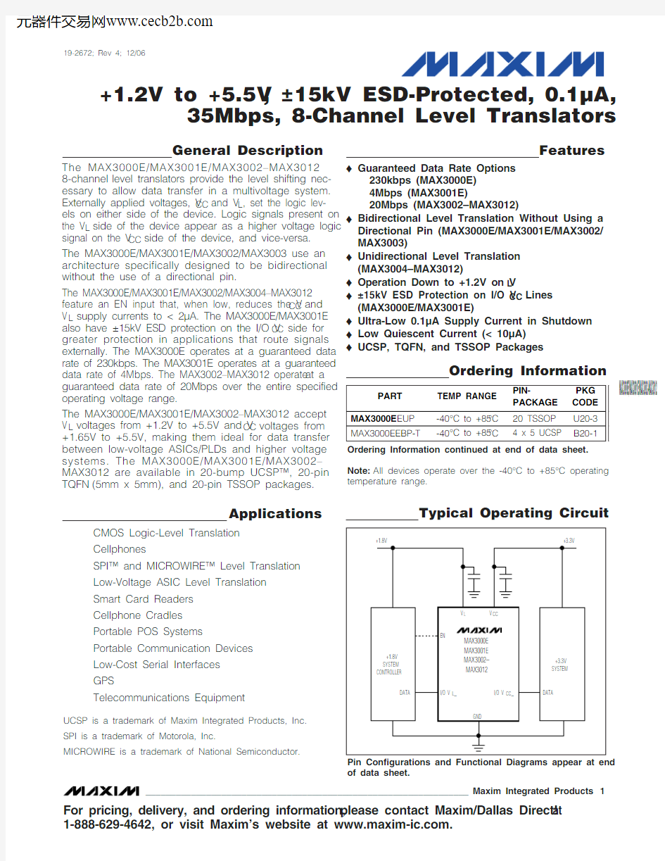
Typical Operating Circuit
19-2672; Rev 4; 12/06
For pricing, delivery, and ordering information,please contact Maxim/Dallas Direct!at 1-888-629-4642, or visit Maxim’s website at https://www.doczj.com/doc/7917287042.html,.
UCSP is a trademark of Maxim Integrated Products, Inc.SPI is a trademark of Motorola, Inc.
MICROWIRE is a trademark of National Semiconductor.
Ordering Information continued at end of data sheet.Pin Configurations and Functional Diagrams appear at end of data sheet.
Note:All devices operate over the -40°C to +85°C operating temperature range.
M A X 3000E /M A X 3001E /M A X 3002–M A X 3012
+1.2V to +5.5V , ±15kV ESD-Protected, 0.1μA,35Mbps, 8-Channel Level Translators 2_______________________________________________________________________________________
ABSOLUTE MAXIMUM RATINGS
Stresses beyond those listed under “Absolute Maximum Ratings” may cause permanent damage to the device. These are stress ratings only, and functional operation of the device at these or any other conditions beyond those indicated in the operational sections of the specifications is not implied. Exposure to absolute maximum rating conditions for extended periods may affect device reliability.
(All voltages referenced to GND.)
V CC ...........................................................................-0.3V to +6V V L...........................................................................................-0.3V to +6V I/O V CC_......................................................-0.3V to (V CC + 0.3V)I/O V L_...........................................................-0.3V to (V L + 0.3V)EN, EN A/B...............................................................-0.3V to +6V Short-Circuit Duration I/O V L_, I/O V CC_to GND .......Continuous Continuous Power Dissipation (T A = +70°C)
20-Pin TSSOP (derate 7.0mW/°C above +70°C).........559mW 20-Bump UCSP (derate 10mW/°C above +70°C).......800mW 20-Pin 5mm x 5mm TQFN
(derate 20.0mW/°C above +70°C)......................................1667mW
Operating Temperature Ranges
MAX3001EAUP..............................................-40°C to +125°C MAX300_EE_P.................................................-40°C to +85°C MAX30_ _E_P ..................................................-40°C to +85°C Junction Temperature......................................................+150°C Storage Temperature Range.............................-65°C to +150°C Lead Temperature (soldering, 10s).................................+300°C
ELECTRICAL CHARACTERISTICS
MAX3000E/MAX3001E/MAX3002–MAX3012
+1.2V to +5.5V , ±15kV ESD-Protected, 0.1μA,
35Mbps, 8-Channel Level Translators
_______________________________________________________________________________________3
ELECTRICAL CHARACTERISTICS (continued)
(V CC = +1.65V to +5.5V, V L = +1.2V to V CC , EN = V L (MAX3000E/MAX3001E/MAX3002/MAX3004–MAX3012), EN A/B = V L or 0(MAX3003), T
= T to T . Typical values are at V = +1.65V, V = +1.2V, and T = +25°C.) (Notes 1, 2)
M A X 3000E /M A X 3001E /M A X 3002–M A X 3012
+1.2V to +5.5V , ±15kV ESD-Protected, 0.1μA,35Mbps, 8-Channel Level Translators 4
_______________________________________________________________________________________
TIMING CHARACTERISTICS
Note 2:For normal operation, ensure that V L < V CC . During power-up, V L > V CC does not damage the device.
MAX3000E/MAX3001E/MAX3002–MAX3012
+1.2V to +5.5V , ±15kV ESD-Protected, 0.1μA,
35Mbps, 8-Channel Level Translators
_______________________________________________________________________________________5
TIMING CHARACTERISTICS (continued)
(V CC = +1.65V to +5.5V, V L = +1.2V to V CC , EN = V L (MAX3000E/MAX3001E/MAX3002/MAX3004–MAX3012), EN A/B = V L or 0(MAX3003), T
= T to T . Typical values are at V = +1.65V, V = +1.2V, and T = +25°C.) (Notes 1, 2)
M A X 3000E /M A X 3001E /M A X 3002–M A X 3012
+1.2V to +5.5V , ±15kV ESD-Protected, 0.1μA,35Mbps, 8-Channel Level Translators 6_______________________________________________________________________________________
TIMING CHARACTERISTICS —MAX3002–MAX3012
(V CC = +1.65V to +5.5V, V L = +1.2V to V CC , EN = V L (MAX3002/MAX3004–MAX3012), EN A/B = V L or 0 (MAX3003), T A = T MIN to T
) (Notes 1, 2)
MAX3000E/MAX3001E/MAX3002–MAX3012
+1.2V to +5.5V , ±15kV ESD-Protected, 0.1μA,
35Mbps, 8-Channel Level Translators
_______________________________________________________________________________________7
Typical Operating Characteristics
(T A = +25°C, unless otherwise noted.)
2000
1500
1000
500
0-40
10
-15
35
60
85
TEMPERATURE (°C)
V L S U P P L Y C U R R E N T (μA )
V L SUPPLY CURRENT vs. TEMPERATURE (DRIVING I/O V CC , V CC = 3.3V, V L = 1.8V)
02000
6000
4000
8000
10,000
1.5
2.5
3.0
2.0
3.5
4.0
4.5
5.0
5.5
SUPPLY VOLTAGE (V)
V C C S U P P L Y C U R R E N T (μA )
V CC SUPPLY CURRENT vs. SUPPLY VOLTAGE
(DRIVING I/O V L , V L = 1.8V)
01002003004005006001.5
2.5
2.0
3.0
3.5
4.0
4.5
5.0
5.5
V L SUPPLY CURRENT vs. SUPPLY VOLTAGE
(DRIVING I/O V L , V L = 1.8V)
SUPPLY VOLTAGE (V)
V L S U P P L Y C U R R E N T (μA )0500
1500
1000
2000
2500-40
10
-15
35
60
85
TEMPERATURE (°C)
V C C S U P P L Y C U R R E N T (μA )
V CC SUPPLY CURRENT vs. TEMPERATURE (DRIVING I/O V CC , V CC = 3.3V, V L = 1.8V)
020
40
60
80
100
10
40
50
20
30
60
70
80
90100
CAPACITIVE LOAD (pF)
V L S U P P L Y C U R R E N T (μA )
V L SUPPLY CURRENT vs. CAPACITIVE LOAD ON I/O V CC (DRIVING I/O V L , V CC = 3.3V, V L = 1.8V)
020001000
4000300060005000700010
30
40
20
50
60
70
80
90
100
CAPACITIVE LOAD (pF)
V C C S U P P L Y C U R R E N T (μA )
V CC SUPPLY CURRENT vs. CAPACITIVE LOAD ON I/O V CC (DRIVING I/O V L , V CC = 3.3V, V L = 1.8V)
CAPACITIVE LOAD (pF)
R I S E /F A L L T I M E (n s )
9080
70
60
50
40
30
20
500
1000
1500
2000
010
100
MAX3000E
RISE/FALL TIME vs. CAPACITIVE LOAD ON I/O V CC (DRIVING I/O V L , V CC = 3.3V, V L = 1.8V)
M A X 3000E /M A X 3001E /M A X 3002–M A X 3012
+1.2V to +5.5V , ±15kV ESD-Protected, 0.1μA,35Mbps, 8-Channel Level Translators 8_______________________________________________________________________________________
Typical Operating Characteristics (continued)
(T A = +25°C, unless otherwise noted.)
010
2030
40506010
30
20
40
50
60
70
80
90100
CAPACITIVE LOAD (pF)
R I S E /F A L L T I M E (n s )
MAX3001E
RISE/FALL TIME vs. CAPACITIVE LOAD ON I/O V CC (DRIVING I/O V L , V CC = 3.3V, V L = 1.8V)
8
6
4
2
010
30
20
40
50
CAPACITIVE LOAD (pF)
R I S E /F A L L T I M E (n s )
MAX3002–MAX3012
RISE/FALL TIME vs. CAPACITIVE LOAD ON I/O V CC (DRIVING I/O V L , V CC = 3.3V, V L = 1.8V)
0500
1000
1500
2000
10
20
60
80
100
CAPACITIVE LOAD (pF)
R I S E /F A L L T I M E (n s )MAX3000E
RISE/FALL TIME vs. CAPACITIVE LOAD ON I/O V L (DRIVING I/O V CC , V CC = 3.3V, V L = 1.8V)
30
40
50
70
90010
203040506010
30
20
40
50
60
70
80
90100
CAPACITIVE LOAD (pF)
R I S E /F A L L T I M E (n s )
MAX3001E
RISE/FALL TIME vs. CAPACITIVE LOAD ON I/O V L (DRIVING I/O V CC , V CC = 3.3V, V L = 1.8V)
43
2
1
10
20
15
25
30
CAPACITIVE LOAD (pF)
R I S E /F A L L T I M E (n s )
MAX3002–MAX3012
RISE/FALL TIME vs. CAPACITIVE LOAD ON I/O V L (DRIVING I/O V CC , V CC = 3.3V, V L = 1.8V)
100
200
300
400
500
10
40
50
20
30
60
70
80
90100
CAPACITIVE LOAD (pF)
P R O P A G A T I O N D E L A Y (n s )
MAX3000E
PROPAGATION DELAY vs. CAPACITIVE LOAD ON I/O V CC (DRIVING I/O V L , V CC = 3.3V, V L = 1.8V)
MAX3000E/MAX3001E/MAX3002–MAX3012
+1.2V to +5.5V , ±15kV ESD-Protected, 0.1μA,
35Mbps, 8-Channel Level Translators
_______________________________________________________________________________________9
Typical Operating Characteristics (continued)
(T A = +25°C, unless otherwise noted.)
100
200300400500600
10
30
20
40
50
60
70
80
90100
CAPACITIVE LOAD (pF)
P R O P A G A T I O N D E L A Y (n s )MAX3000E
PROPAGATION DELAY vs. CAPACITIVE LOAD ON I/O V L (DRIVING I/O V CC , V CC = 3.3V, V L = 1.8V)
03
9
6
12
15
CAPACITIVE LOAD (pF)
P R O P A G A T I O N D E L A Y (n s )
10
30
20
40
50
MAX3001E
PROPAGATION DELAY vs. CAPACITIVE LOAD ON I/O V L (DRIVING I/O V CC , V CC = 3.3V, V L = 1.8V)
01
3
2
4
5
CAPACITIVE LOAD (pF)
P R O P A G A T I O N D E L A Y (n s
)
10
20
15
25
30
MAX3002–MAX3012
PROPAGATION DELAY vs. CAPACITIVE LOAD ON I/O V L (DRIVING I/O V CC , V CC = 3.3V, V L = 1.8V)
1μs/div
MAX3000E RAIL-TO-RAIL DRIVING (DRIVING I/O V L , V CC = 3.3V, V L = 1.8V,CV CC = 50pF, DATA RATE = 230kbps)
GND
I/O V L_1V/div GND
MAX3000E/01E/02-12 toc19
I/O V CC_2V/div 40ns/div
MAX3001E RAIL-TO-RAIL DRIVING (DRIVING I/O V L , V CC = 3.3V, V L = 1.8V,CV CC = 50pF, DATA RATE = 4Mbps)
GND
I/O V L_1V/div GND
MAX3000E/01E/02-12 toc20
I/O V CC_2V/div 10ns/div
MAX3002–MAX3012 RAIL-TO-RAIL DRIVING (DRIVING I/O V L , V CC = 3.3V, V L = 1.8V,CV CC = 50pF, DATA RATE = 20Mbps)
GND
I/O V L_1V/div GND
MAX3000E/01E/02-12 toc21
I/O V CC_2V/div 0105
20
15253010
30
20
4050CAPACITIVE LOAD (pF)P R O P A G A T I O N D E L A Y (n s )
MAX3001E
PROPAGATION DELAY vs. CAPACITIVE LOAD ON I/O V CC (DRIVING I/O V L , V CC = 3.3V, V L = 1.8V)
42
8610
1210201525
30
CAPACITIVE LOAD (pF)P R O P A G A T I O N D E L A Y (n s )
MAX3002–MAX3012
PROPAGATION DELAY vs. CAPACITIVE LOAD ON I/O V CC (DRIVING I/O V L , V CC = 3.3V, V L = 1.8V)
M A X 3000E /M A X 3001E /M A X 3002–M A X 3012
+1.2V to +5.5V , ±15kV ESD-Protected, 0.1μA,35Mbps, 8-Channel Level Translators 10______________________________________________________________________________________
Pin Description
MAX3000E/MAX3001E/MAX3002
MAX3000E/MAX3001E/MAX3002–MAX3012
+1.2V to +5.5V , ±15kV ESD-Protected, 0.1μA,
35Mbps, 8-Channel Level Translators
______________________________________________________________________________________11
Pin Description (continued)
M A X 3000E /M A X 3001E /M A X 3002–M A X 3012
+1.2V to +5.5V , ±15kV ESD-Protected, 0.1μA,35Mbps, 8-Channel Level Translators 12______________________________________________________________________________________
Pin Description (continued)
MAX3004–MAX3012
MAX3000E/MAX3001E/MAX3002–MAX3012
+1.2V to +5.5V , ±15kV ESD-Protected, 0.1μA,
35Mbps, 8-Channel Level Translators
______________________________________________________________________________________13
______________________________________________Test Circuits/Timing Diagrams
Figure 1a. Driving I/O V L Figure 1b. Timing for Driving I/O V L
Figure 2a. Driving I/O V CC
Figure 2b. Timing for Driving I/O V CC
M A X 3000E /M A X 3001E /M A X 3002–M A X 3012
+1.2V to +5.5V , ±15kV ESD-Protected, 0.1μA,35Mbps, 8-Channel Level Translators 14
______________________________________________________________________________________
_________________________________Test Circuits/Timing Diagrams (continued)
Figure 3. Propagation Delay from I/O V L to I/O V CC After EN
Figure 4. Propagation Delay from I/O V CC to I/O V L After EN
MAX3000E/MAX3001E/MAX3002–MAX3012
+1.2V to +5.5V , ±15kV ESD-Protected, 0.1μA,
35Mbps, 8-Channel Level Translators
______________________________________________________________________________________
15
Detailed Description
The MAX3000E/MAX3001E/MAX3002–MAX3012 logic-level translators provide the level shifting necessary to allow data transfer in a multivoltage system. Externally applied voltages, V CC and V L , set the logic levels on either side of the device. Logic signals present on the V L side of the device appear as a higher voltage logic signal on the V CC side of the device, and vice-versa.The MAX3000E/MAX3001E/MAX3002/MAX3003 are bidirectional level translators allowing data translation in either direction (V L ?V CC ) on any single data line.These devices use an architecture specifically designed to be bidirectional without the use of a direc-tion pin. The MAX3004–MAX3012 unidirectional level translators level shift data in one direction (V L →V CC or V CC →V L ) on any single data line. The MAX3000E/MAX3001E/ MAX3002–MAX3012 accept V L from +1.2V to +5.5V. All devices have V CC ranging from +1.65V to +5.5V, making them ideal for data trans-fer between low-voltage ASICs/PLDs and higher volt-age systems.
The MAX3000E/MAX3001E/MAX3002/MAX3004–MAX3012 feature an output enable mode that reduces V CC supply current to less than 2μA, and V L supply current to less than 2μA when in shutdown. The MAX3000E/MAX3001E have ±15kV ESD protection on the V CC side for greater protection in applications that route signals externally. The MAX3000E operates at a guaranteed data rate of 230kbps; the MAX3001E oper-ates at a guaranteed data rate of 4Mbps and the MAX3002–MAX3012 are guaranteed with a data rate of 20Mbps of operation over the entire specified operating voltage range.
Level Translation
For proper operation, ensure that +1.65V ≤V CC ≤+5.5V,+1.2V ≤V L ≤+5.5V, and V L ≤V CC . During power-up sequencing, V L ≥V CC does not damage the device.During power-supply sequencing, when V CC is floating and V L is powering up, up to 10mA current can be sourced to each load on the V L side, yet the device does not latch up.
The maximum data rate also depends heavily on the load capacitance (see the Typical O perating Characteristics ), output impedance of the driver, and the operational voltage range (see the Timing Characteristics table).
Input Driver Requirements
The MAX3001E/MAX3002–MAX3012 architecture is based on a one-shot accelerator output stage. See Figure 5. Accelerator output stages are always in three-
state except when there is a transition on any of the translators on the input side, either I/O V L or I/O V CC . When there is such a transition, the accelerator stages become active, charging (discharging) the capacitances at the I/Os. Due to its bidirectional nature, both stages become active during the one-shot pulse. This can lead to some current feeding into the external source that is driving the translator. However, this behavior helps to speed up the transition on the driven side.
F or proper full-speed operation, the output current of a device that drives the inputs of the MAX3000E/MAX3001E/MAX3002–MAX3012 should meet the fol-lowing requirements:
?MAX3000E (230kbps):i > 1mA, R drv < 1k ??MAX3001E (4Mbps):i > 107x V x (C + 10pF)
?MAX3002–MAX3012 (20Mbps):i > 108x V x (C + 10pF)
where i is the driver output current, V is the logic-supply voltage (i.e., V L or V CC ) and C is the parasitic capaci-tance of the signal line.
Enable Output Mode (EN, EN A/B)
The MAX3000E/MAX3001E/MAX3002 and the MAX3004–MAX3012 feature an EN input, and the MAX3003 has an EN A/B input. Pull EN low to set the MAX3000E/MAX3001E/MAX3002/MAX3004–MAX3012s ’ I/O V CC 1through I/O V CC 8 in three-state output mode, while I/O V L 1 through I/O V L 8 have internal 6k ?pulldown resis-tors. Drive EN to logic-high (V L ) for normal operation. The MAX3003 is intended for bus multiplexing or bus switch-ing applications. Drive EN A/B low to place channels 1B through 4B in active mode, while channels 1A through 4A are in three-state mode. Drive EN A/B to logic-high (V L ) to enable channels 1A through 4A, while channels 1B through 4B remain in three-state mode.
±15kV ESD Protection
As with all Maxim devices, ESD-protection structures are incorporated on all pins to protect against electro-static discharges encountered during handling and assembly. The I/O V CC lines have extra protection against static discharge. Maxim ’s engineers have developed state-of-the-art structures to protect these pins against ESD of ±15kV without damage. The ESD structures withstand high ESD in all states: normal operation, three-state output mode, and powered down. After an ESD event, Maxim ’s E versions keep working without latchup, whereas competing products can latch and must be powered down to remove latchup.
M A X 3000E /M A X 3001E /M A X 3002–M A X 3012
+1.2V to +5.5V , ±15kV ESD-Protected, 0.1μA,35Mbps, 8-Channel Level Translators 16
______________________________________________________________________________________
ESD protection can be tested in various ways. The I/O V CC lines of the MAX3000E/MAX3001E are char-acterized for protection to ±15kV using the Human Body Model.
ESD Test Conditions
ESD performance depends on a variety of conditions.Contact Maxim for a reliability report that documents test setup, test methodology, and test results.
Human Body Model
Figure 7a shows the Human Body Model and Figure 7b shows the current waveform it generates when dis-charged into a low impedance. This model consists of a 100pF capacitor charged to the ESD voltage of inter-est, which is then discharged into the test device through a 1.5k ?resistor.
Machine Model
The Machine Model for ESD tests all pins using a 200pF storage capacitor and zero discharge resis-tance. Its objective is to emulate the stress caused by contact that occurs with handling and assembly during manufacturing. Of course, all pins require this protec-tion during manufacturing, not just inputs and outputs.Therefore, after PCB assembly, the Machine Model is less relevant to I/O ports.
Figure 5. MAX3001E/MAX3002–MAX3012 Simplified Functional Diagram (1 I/O Line)
Figure 6. Typical I IN vs. V IN
Applications Information
Power-Supply Decoupling To reduce ripple and the chance of transmitting incor-rect data, bypass V L and V CC to ground with a 0.1μF capacitor. To ensure full ±15kV ESD protection, bypass V CC to ground with a 1μF capacitor. Place all capaci-tors as close to the power-supply inputs as possible.
I2C Level Translation For I2C level translation for I2C applications, please refer to the MAX3372E–MAX3379E/MAX3390E–MAX3393E datasheet.
Unidirectional vs. Bidirectional Level
Translator
The MAX3000E/MAX3001E/MAX3002/MAX3003 bidi-rectional translators can operate as a unidirectional device to translate signals without inversion. The
MAX3004–MAX3012 unidirecitional level translators,
level-shift data in one direction (V L→V CC or V CC→V L)
on any single data line (see the Ordering Information.) These devices provide the smallest solution (UCSP package) for unidirectional level translation without inversion. MAX3000E/MAX3001E/MAX3002–MAX3012
+1.2V to +5.5V, ±15kV ESD-Protected, 0.1μA, 35Mbps, 8-Channel Level Translators
______________________________________________________________________________________17
M A X 3000E /M A X 3001E /M A X 3002–M A X 3012
+1.2V to +5.5V , ±15kV ESD-Protected, 0.1μA,35Mbps, 8-Channel Level Translators
Figure 7a. Human Body ESD Test Model Figure 7b. Human Body Current Waveform
Selector Guide
**See Table 1.
Table 1. Data Rate
MAX3000E/MAX3001E/MAX3002–MAX3012
+1.2V to +5.5V , ±15kV ESD-Protected, 0.1μA,
35Mbps, 8-Channel Level Translators
MAX3000E/MAX3001E/MAX3002 Functional Diagram
M A X 3000E /M A X 3001E /M A X 3002–M A X 3012
+1.2V to +5.5V , ±15kV ESD-Protected, 0.1μA,35Mbps, 8-Channel Level Translators
MAX3003 Functional Diagram