FEATURES
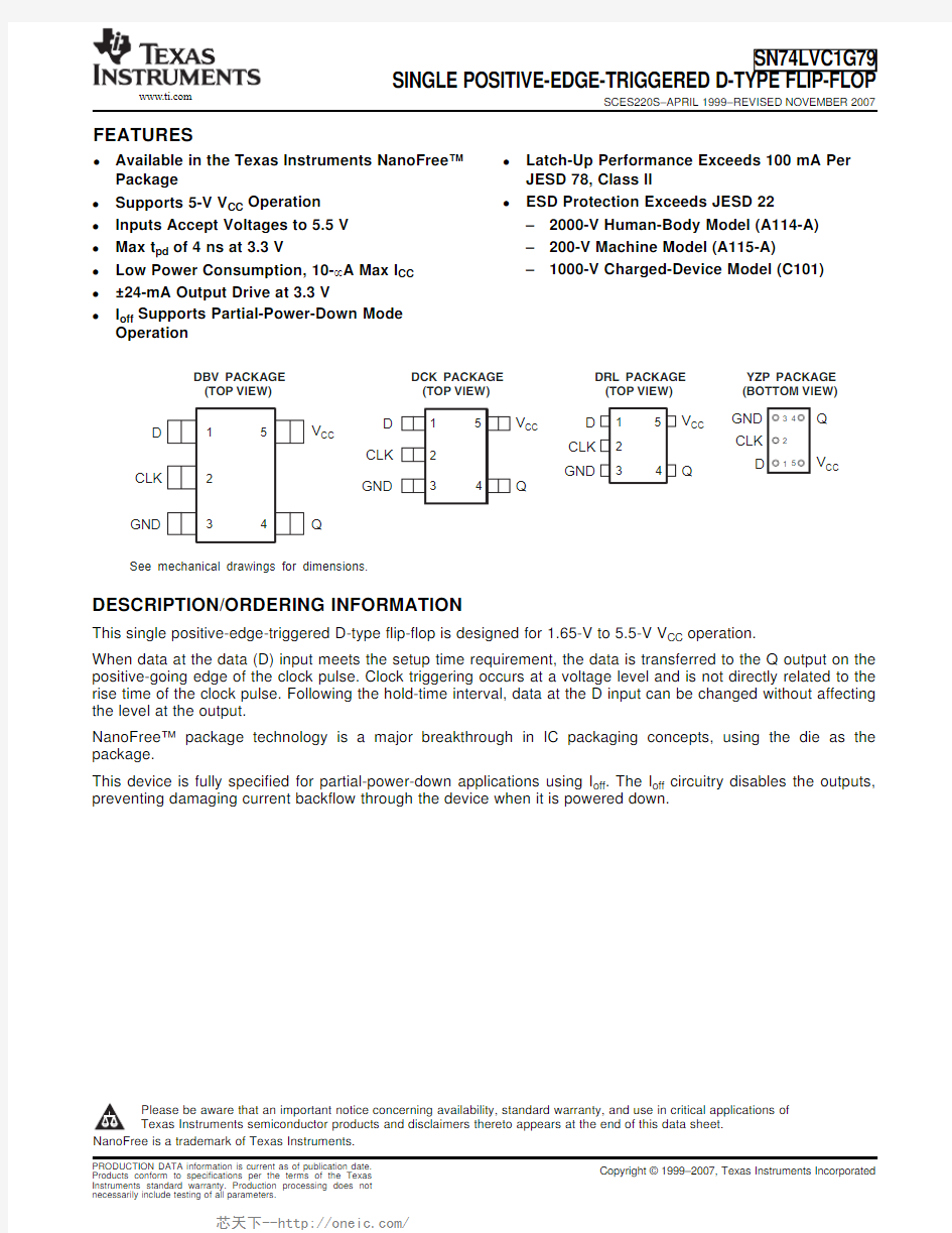
See mechanical drawings for dimensions.
DBV PACKAGE (TOP VIEW)5
1V CC
D 2
CLK 34
GND
Q
DRL PACKAGE (TOP VIEW)2CLK V CC 5
1D 3
4
GND
Q
DCK PACKAGE (TOP VIEW)2CLK
3
4GND
V CC
5
D Q
1YZP PACKAGE (BOTTOM
VIEW)
CLK V CC
GND Q DESCRIPTION/ORDERING
INFORMATION
SN74LVC1G79
SINGLE POSITIVE-EDGE-TRIGGERED D-TYPE FLIP-FLOP
SCES220S–APRIL 1999–REVISED NOVEMBER 2007
https://www.doczj.com/doc/768658274.html,
?Available in the Texas Instruments NanoFree??Latch-Up Performance Exceeds 100mA Per Package
JESD 78,Class II
?Supports 5-V V CC Operation ?
ESD Protection Exceeds JESD 22
?Inputs Accept Voltages to 5.5V –2000-V Human-Body Model (A114-A)?Max t pd of 4ns at 3.3V
–200-V Machine Model (A115-A)
?Low Power Consumption,10-μA Max I CC –1000-V Charged-Device Model (C101)
?±24-mA Output Drive at 3.3V
?I off Supports Partial-Power-Down Mode Operation
This single positive-edge-triggered D-type flip-flop is designed for 1.65-V to 5.5-V V CC operation.
When data at the data (D)input meets the setup time requirement,the data is transferred to the Q output on the positive-going edge of the clock pulse.Clock triggering occurs at a voltage level and is not directly related to the rise time of the clock pulse.Following the hold-time interval,data at the D input can be changed without affecting the level at the output.
NanoFree?package technology is a major breakthrough in IC packaging concepts,using the die as the package.
This device is fully specified for partial-power-down applications using I off .The I off circuitry disables the outputs,preventing damaging current backflow through the device when it is powered down.
Please be aware that an important notice concerning availability,standard warranty,and use in critical applications of Texas Instruments semiconductor products and disclaimers thereto appears at the end of this data sheet.
NanoFree is a trademark of Texas Instruments.
PRODUCTION DATA information is current as of publication date.Copyright ?1999–2007,Texas Instruments Incorporated
Products conform to specifications per the terms of the Texas Instruments standard warranty.Production processing does not necessarily include testing of all parameters.
https://www.doczj.com/doc/768658274.html,
CLK
Q
SN74LVC1G79
SINGLE POSITIVE-EDGE-TRIGGERED D-TYPE FLIP-FLOP
SCES220S–APRIL 1999–REVISED NOVEMBER 2007
ORDERING INFORMATION
T A
PACKAGE (1)(2)
ORDERABLE PART NUMBER TOP-SIDE MARKING (3)NanoFree?–WCSP (DSBGA)0.23-mm Large Bump –YZP Reel of 3000SN74LVC1G79YZPR ___CR_
(Pb-free)
Reel of 3000SN74LVC1G79DBVR SOT (SOT-23)–DBV C79_–40°C to 85°C
Reel of 250SN74LVC1G79DBVT Reel of 3000SN74LVC1G79DCKR SOT (SC-70)–DCK CR_Reel of 250SN74LVC1G79DCKT SOT (DOT-553)–DRL
Reel of 4000
SN74LVC1G79DRLR
CR_
(1)Package drawings,thermal data,and symbolization are available at https://www.doczj.com/doc/768658274.html,/packaging .
(2)For the most current package and ordering information,see the Package Option Addendum at the end of this document,or see the TI website at https://www.doczj.com/doc/768658274.html, .
(3)
DBV/DCK/DRL:The actual top-side marking has one additional character that designates the assembly/test site.
YZP:The actual top-side marking has three preceding characters to denote year,month,and sequence code,and one following character to designate the assembly/test site.Pin 1identifier indicates solder-bump composition (1=SnPb,?=Pb-free).
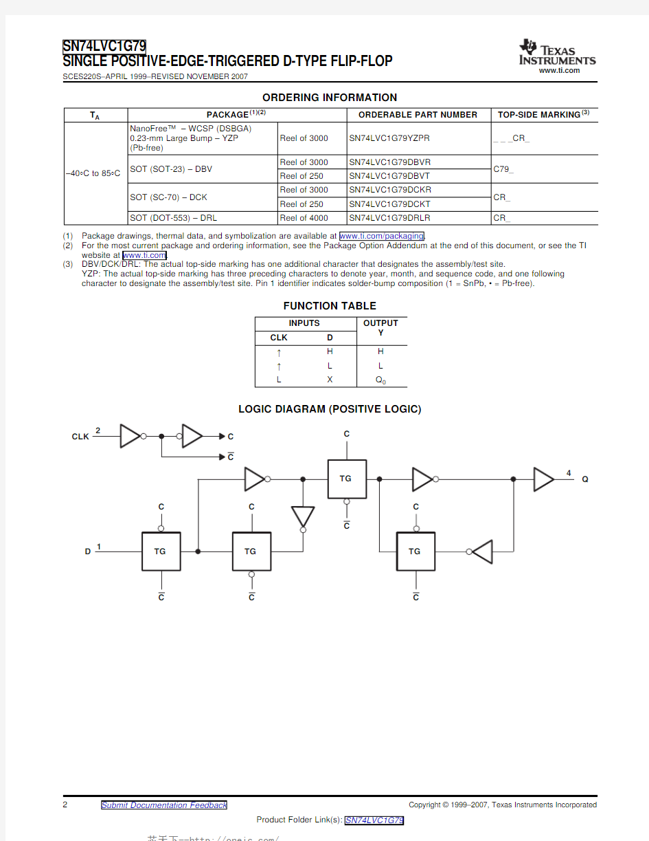
FUNCTION TABLE
INPUTS OUTPUT
Y
CLK D ↑H H ↑L L L
X
Q 0
LOGIC DIAGRAM (POSITIVE LOGIC)
2Submit Documentation Feedback
Copyright ?1999–2007,Texas Instruments Incorporated
Product Folder Link(s):SN74LVC1G79
https://www.doczj.com/doc/768658274.html,
Absolute Maximum Ratings(1)
SN74LVC1G79 SINGLE POSITIVE-EDGE-TRIGGERED D-TYPE FLIP-FLOP
SCES220S–APRIL1999–REVISED NOVEMBER2007
over operating free-air temperature range(unless otherwise noted)
MIN MAX UNIT
V CC Supply voltage range–0.5 6.5V
V I Input voltage range(2)–0.5 6.5V
V O Voltage range applied to any output in the high-impedance or power-off state(2)–0.5 6.5V
V O Voltage range applied to any output in the high or low state(2)(3)–0.5V CC+0.5V
I IK Input clamp current V I<0–50mA
I OK Output clamp current V O<0–50mA
I O Continuous output current±50mA
Continuous current through V CC or GND±100mA
DBV package206
DCK package252
θJA Package thermal impedance(4)°C/W
DRL package142
YZP package132
T stg Storage temperature range–65150°C (1)Stresses beyond those listed under"absolute maximum ratings"may cause permanent damage to the device.These are stress ratings
only,and functional operation of the device at these or any other conditions beyond those indicated under"recommended operating conditions"is not implied.Exposure to absolute-maximum-rated conditions for extended periods may affect device reliability.
(2)The input negative-voltage and output voltage ratings may be exceeded if the input and output current ratings are observed.
(3)The value of V CC is provided in the recommended operating conditions table.
(4)The package thermal impedance is calculated in accordance with JESD51-7.
Copyright?1999–2007,Texas Instruments Incorporated Submit Documentation Feedback3
Product Folder Link(s):SN74LVC1G79
https://www.doczj.com/doc/768658274.html,
Recommended Operating Conditions (1)
SN74LVC1G79
SINGLE POSITIVE-EDGE-TRIGGERED D-TYPE FLIP-FLOP
SCES220S–APRIL 1999–REVISED NOVEMBER 2007
MIN
MAX UNIT Operating
1.65 5.5
V CC
Supply voltage
V
Data retention only 1.5
V CC =1.65V to 1.95V
0.65×V CC
V CC =2.3V to 2.7V 1.7V IH
High-level input voltage
V
V CC =3V to 3.6V 2
V CC =4.5V to 5.5V 0.7×V CC
V CC =1.65V to 1.95V
0.35×V CC
V CC =2.3V to 2.7V 0.7V IL
Low-level input voltage
V V CC =3V to 3.6V 0.8V CC =4.5V to 5.5V
0.3×V CC
V I Input voltage 0 5.5V V O
Output voltage
0V CC V V CC =1.65V –4V CC =2.3V
–8I OH
High-level output current
–16mA V CC =3V –24V CC =4.5V –32V CC =1.65V 4V CC =2.3V
8I OL
Low-level output current
16mA V CC =3V 24V CC =4.5V
32V CC =1.8V ±0.15V,2.5V ±0.2V
20Δt/Δv Input transition rise or fall rate V CC =3.3V ±0.3V 10ns/V V CC =5V ±0.5V
5T A Operating free-air temperature
–4085
°C (1)
All unused inputs of the device must be held at V CC or GND to ensure proper device operation.Refer to the TI application report,Implications of Slow or Floating CMOS Inputs ,literature number SCBA004.
4Submit Documentation Feedback
Copyright ?1999–2007,Texas Instruments Incorporated
Product Folder Link(s):SN74LVC1G79
https://www.doczj.com/doc/768658274.html,
Electrical Characteristics Timing Requirements
SN74LVC1G79 SINGLE POSITIVE-EDGE-TRIGGERED D-TYPE FLIP-FLOP
SCES220S–APRIL1999–REVISED NOVEMBER2007
over recommended operating free-air temperature range(unless otherwise noted)
PARAMETER TEST CONDITIONS V CC MIN TYP(1)MAX UNIT
I OH=–100μA 1.65V to5.5V V CC–0.1
I OH=–4mA 1.65V 1.2
I OH=–8mA 2.3V 1.9
V OH V
I OH=–16mA 2.4
3V
I OH=–24mA 2.3
I OH=–32mA 4.5V 3.8
I OL=100μA 1.65V to5.5V0.1
I OL=4mA 1.65V0.45
I OL=8mA 2.3V0.3
V OL V
I OL=16mA0.4
3V
I OL=24mA0.55
I OL=32mA 4.5V0.55
I I All inputs V I=5.5V or GND0to5.5V±10μA
I off V I or V O=5.5V0±10μA
I CC V I=5.5V or GND,I O=0 1.65V to5.5V10μA
ΔI CC One input at V CC–0.6V,Other inputs at V CC or GND3V to5.5V500μA
C i V I=V CC or GN
D 3.3V4pF
(1)All typical values are at V CC=3.3V,T A=25°C.
over operating free-air temperature range(unless otherwise noted)(see Figure1)
V CC=1.8V CC=2.5V CC=3.3V V CC=5V
±0.15V±0.2V±0.3V±0.5V
PARAMETER UNIT
MIN MAX MIN MAX MIN MAX MIN MAX
f clock Clock frequency160160160160MHz
t w Pulse duration,CLK high or low 2.5 2.5 2.5 2.5ns
Data high 2.2 1.4 1.3 1.2
t su Setup time before CLK↑ns
Data low 2.6 1.4 1.3 1.2
t h Hold time,data after CLK↑0.30.410.5ns
Copyright?1999–2007,Texas Instruments Incorporated Submit Documentation Feedback5
Product Folder Link(s):SN74LVC1G79
https://www.doczj.com/doc/768658274.html,
Switching Characteristics
Switching Characteristics
Operating Characteristics
SN74LVC1G79
SINGLE POSITIVE-EDGE-TRIGGERED D-TYPE FLIP-FLOP
SCES220S–APRIL 1999–REVISED NOVEMBER 2007
over recommended operating free-air temperature range,C L =15pF (unless otherwise noted)(see Figure 1)
V CC =1.8V V CC =2.5V V CC =3.3V V CC =5V FROM TO ±0.15V ±0.2V ±0.3V ±0.5V PARAMETER
UNIT
(INPUT)
(OUTPUT)
MIN MAX
MIN MAX
MIN MAX
MIN MAX
f max 160160160160MHz t pd
CLK
Q
2.5
9.1 1.2
61
40.8
3.8ns over recommended operating free-air temperature range,C L =30pF or 50pF (unless otherwise noted)(see Figure 2)
V CC =1.8V V CC =2.5V V CC =3.3V V CC =5V FROM TO ±0.15V ±0.2V ±0.3V ±0.5V PARAMETER
UNIT
(INPUT)
(OUTPUT)
MIN MAX
MIN MAX
MIN MAX
MIN MAX
f max 160160160160MHz t pd
CLK
Q
3.9
9.92
7 1.7
51
4.5ns T A =25°C
V CC =1.8V
V CC =2.5V
V CC =3.3V
V CC =5V TEST PARAMETER
UNIT CONDITIONS TYP TYP TYP TYP C pd
Power dissipation capacitance
f =10MHz
26
26
27
30
pF
6Submit Documentation Feedback
Copyright ?1999–2007,Texas Instruments Incorporated
Product Folder Link(s):SN74LVC1G79
https://www.doczj.com/doc/768658274.html,
PARAMETER MEASUREMENT INFORMATION
From Output
Under Test
(see Note
LOAD CIRCUIT
V
Open
Data Input
Timing Input
0 V
0 V
0 V
Input
0 V
Input
Output
Waveform 1
S1 at V
(see Note B)
LOAD
Output
Waveform 2
S1 at GND
(see Note B)
V
OL
V
OH
0 V
?0 V Output
Output
t/t
PLH PHL
Open
TEST S1
Output
Control
1.8 V0.15 V
±
2.5 V0.2 V
±
3.3 V0.3 V
±
5 V0.5 V
±
1 M W
1 M W
1 M W
1 M W
V
CC
R
L
2 ×V
CC
2 ×V
CC
6 V
2 ×V
CC
V
LOAD
C
L
15 pF
15 pF
15 pF
15 pF
0.15 V
0.15 V
0.3 V
0.3 V
V
D
3 V
V
I
V
CC
/2
V
CC
/2
1.5 V
V
CC
/2
V
M
£2 ns
£2 ns
£2.5 ns
£2.5 ns
INPUTS
t/t
r f
V
CC
V
CC
V
CC
V
LOAD
t/t
PLZ PZL
GND
t/t
PHZ PZH
VOLTAGE WAVEFORMS
ENABLE AND DISABLE TIMES
LOW-AND HIGH-LEVEL ENABLING
VOLTAGE WAVEFORMS
PROPAGATION DELAY TIMES
INVERTING AND NONINVERTING OUTPUTS
NOTES: A.C includes probe and jig capacitance.
B.Waveform 1 is for an output with internal conditions such that the output is low, except when disabled by the output control.
Waveform 2 is for an output with internal conditions such that the output is high, except when disabled by the output control.
C.All input pulses are supplied by generators having the following characteristics: PRR10 MHz, Z= 50.
D.The outputs are measured one at a time, with one transition per measurement.
E.t and t are the same as t.
F.t and t are the same as t.
G.t and t are the same as t.
H.All parameters and waveforms are not applicable to all devices.
L
O
PLZ PHZ dis
PZL PZH en
PLH PHL pd
£W
VOLTAGE WAVEFORMS
PULSE DURATION
VOLTAGE WAVEFORMS
SETUP AND HOLD TIMES
V
I
V
I
V
I
V/2
LOAD
V
OL
V
OH
V
I
V
I
V
OH
V
OL
SN74LVC1G79
SINGLE POSITIVE-EDGE-TRIGGERED D-TYPE FLIP-FLOP
SCES220S–APRIL1999–REVISED NOVEMBER2007
Figure1.Load Circuit and Voltage Waveforms
Copyright?1999–2007,Texas Instruments Incorporated Submit Documentation Feedback7
Product Folder Link(s):SN74LVC1G79
https://www.doczj.com/doc/768658274.html,
From Output
Under Test
(see Note
LOAD CIRCUIT
Open
Data Input
Timing Input
0 V
0 V
0 V
Input
0 V
Input
Output
Waveform 1
S1 at V
(see Note B)
LOAD
Output
Waveform 2
S1 at GND
(see Note B)
V
OL
V
OH
0 V
?0 V Output
Output
TEST S1
t/t
PLH PHL
Open
Output
Control
1.8 V0.15 V
±
2.5 V0.2 V
±
3.3 V0.3 V
±
5 V0.5 V
±
1 k W
500W
500W
500W
V
CC
R
L
2 ×V
CC
2 ×V
CC
6 V
2 ×V
CC
V
LOAD
C
L
30 pF
30 pF
50 pF
50 pF
0.15 V
0.15 V
0.3 V
0.3 V
V
D
3 V
V
I
V
CC
/2
V
CC
/2
1.5 V
V
CC
/2
V
M
£2 ns
£2 ns
£2.5 ns
£2.5 ns
INPUTS
t/t
r f
V
CC
V
CC
V
CC
V
LOAD
t/t
PLZ PZL
GND
t/t
PHZ PZH
VOLTAGE WAVEFORMS
ENABLE AND DISABLE TIMES
LOW-AND HIGH-LEVEL ENABLING
VOLTAGE WAVEFORMS
PROPAGATION DELAY TIMES
INVERTING AND NONINVERTING OUTPUTS
NOTES: A.C includes probe and jig capacitance.
B.Waveform 1 is for an output with internal conditions such that the output is low, except when disabled by the output control.
Waveform 2 is for an output with internal conditions such that the output is high, except when disabled by the output control.
C.All input pulses are supplied by generators having the following characteristics: PRR10 MHz, Z= 50.
D.The outputs are measured one at a time, with one transition per measurement.
E.t and t are the same as t.
F.t and t are the same as t.
G.t and t are the same as t.
H.All parameters and waveforms are not applicable to all devices.
L
O
PLZ PHZ dis
PZL PZH en
PLH PHL pd
£W
VOLTAGE WAVEFORMS
PULSE DURATION
VOLTAGE WAVEFORMS
SETUP AND HOLD TIMES
V
I
V
I
V
I
V/2
LOAD
V
OL
V
OH
V
I
V
I
V
OH
V
OL
SN74LVC1G79
SINGLE POSITIVE-EDGE-TRIGGERED D-TYPE FLIP-FLOP
SCES220S–APRIL1999–REVISED NOVEMBER2007
PARAMETER MEASUREMENT INFORMATION(continued)
Figure2.Load Circuit and Voltage Waveforms
8Submit Documentation Feedback Copyright?1999–2007,Texas Instruments Incorporated
Product Folder Link(s):SN74LVC1G79
PACKAGING INFORMATION
Orderable Device Status(1)Package
Type Package
Drawing
Pins Package
Qty
Eco Plan(2)Lead/Ball Finish MSL Peak Temp(3)
SN74LVC1G79DBVR ACTIVE SOT-23DBV53000Green(RoHS&
no Sb/Br)
CU NIPDAU Level-1-260C-UNLIM
SN74LVC1G79DBVRE4ACTIVE SOT-23DBV53000Green(RoHS&
no Sb/Br)
CU NIPDAU Level-1-260C-UNLIM
SN74LVC1G79DBVRG4ACTIVE SOT-23DBV53000Green(RoHS&
no Sb/Br)
CU NIPDAU Level-1-260C-UNLIM
SN74LVC1G79DBVT ACTIVE SOT-23DBV5250Green(RoHS&
no Sb/Br)
CU NIPDAU Level-1-260C-UNLIM
SN74LVC1G79DBVTE4ACTIVE SOT-23DBV5250Green(RoHS&
no Sb/Br)
CU NIPDAU Level-1-260C-UNLIM
SN74LVC1G79DBVTG4ACTIVE SOT-23DBV5250Green(RoHS&
no Sb/Br)
CU NIPDAU Level-1-260C-UNLIM
SN74LVC1G79DCKR ACTIVE SC70DCK53000Green(RoHS&
no Sb/Br)
CU NIPDAU Level-1-260C-UNLIM
SN74LVC1G79DCKRE4ACTIVE SC70DCK53000Green(RoHS&
no Sb/Br)
CU NIPDAU Level-1-260C-UNLIM
SN74LVC1G79DCKRG4ACTIVE SC70DCK53000Green(RoHS&
no Sb/Br)
CU NIPDAU Level-1-260C-UNLIM
SN74LVC1G79DCKT ACTIVE SC70DCK5250Green(RoHS&
no Sb/Br)
CU NIPDAU Level-1-260C-UNLIM
SN74LVC1G79DCKTE4ACTIVE SC70DCK5250Green(RoHS&
no Sb/Br)
CU NIPDAU Level-1-260C-UNLIM
SN74LVC1G79DCKTG4ACTIVE SC70DCK5250Green(RoHS&
no Sb/Br)
CU NIPDAU Level-1-260C-UNLIM
SN74LVC1G79DRLR ACTIVE SOT DRL54000Green(RoHS&
no Sb/Br)
CU NIPDAU Level-1-260C-UNLIM
SN74LVC1G79DRLRG4ACTIVE SOT DRL54000Green(RoHS&
no Sb/Br)
CU NIPDAU Level-1-260C-UNLIM
SN74LVC1G79YZPR ACTIVE DSBGA YZP53000Green(RoHS&
no Sb/Br)
SNAGCU Level-1-260C-UNLIM
(1)The marketing status values are defined as follows:
ACTIVE:Product device recommended for new designs.
LIFEBUY:TI has announced that the device will be discontinued,and a lifetime-buy period is in effect.
NRND:Not recommended for new designs.Device is in production to support existing customers,but TI does not recommend using this part in a new design.
PREVIEW:Device has been announced but is not in production.Samples may or may not be available.
OBSOLETE:TI has discontinued the production of the device.
(2)Eco Plan-The planned eco-friendly classification:Pb-Free(RoHS),Pb-Free(RoHS Exempt),or Green(RoHS&no Sb/Br)-please check https://www.doczj.com/doc/768658274.html,/productcontent for the latest availability information and additional product content details.
TBD:The Pb-Free/Green conversion plan has not been defined.
Pb-Free(RoHS):TI's terms"Lead-Free"or"Pb-Free"mean semiconductor products that are compatible with the current RoHS requirements for all6substances,including the requirement that lead not exceed0.1%by weight in homogeneous materials.Where designed to be soldered at high temperatures,TI Pb-Free products are suitable for use in specified lead-free processes.
Pb-Free(RoHS Exempt):This component has a RoHS exemption for either1)lead-based flip-chip solder bumps used between the die and package,or2)lead-based die adhesive used between the die and leadframe.The component is otherwise considered Pb-Free(RoHS compatible)as defined above.
Green(RoHS&no Sb/Br):TI defines"Green"to mean Pb-Free(RoHS compatible),and free of Bromine(Br)and Antimony(Sb)based flame retardants(Br or Sb do not exceed0.1%by weight in homogeneous material)
(3)MSL,Peak Temp.--The Moisture Sensitivity Level rating according to the JEDEC industry standard classifications,and peak solder temperature.
Important Information and Disclaimer:The information provided on this page represents TI's knowledge and belief as of the date that it is provided.TI bases its knowledge and belief on information provided by third parties,and makes no representation or warranty as to the accuracy of such information.Efforts are underway to better integrate information from third parties.TI has taken and continues to take reasonable steps to provide representative and accurate information but may not have conducted destructive testing or chemical analysis on incoming materials and chemicals.TI and TI suppliers consider certain information to be proprietary,and thus CAS numbers and other limited information may not be available for release.
In no event shall TI's liability arising out of such information exceed the total purchase price of the TI part(s)at issue in this document sold by TI to Customer on an annual basis.
OTHER QUALIFIED VERSIONS OF SN74LVC1G79:
?Enhanced Product:SN74LVC1G79-EP
NOTE:Qualified Version Definitions:
?Enhanced Product-Supports Defense,Aerospace and Medical Applications
TAPE AND REEL INFORMATION
*All dimensions are nominal
Device
Package Type Package Drawing Pins SPQ
Reel Diameter (mm)Reel Width W1(mm)A0(mm)B0(mm)K0(mm)P1(mm)W (mm)Pin1Quadrant SN74LVC1G79DBVR SOT-23DBV 53000178.09.2 3.3 3.2 1.55 4.08.0Q3SN74LVC1G79DBVR SOT-23DBV 53000178.09.0 3.23 3.17 1.37 4.08.0Q3SN74LVC1G79DBVT SOT-23DBV 5250178.09.2 3.3 3.2 1.55 4.08.0Q3SN74LVC1G79DBVT SOT-23DBV 5250178.09.0 3.23 3.17 1.37 4.08.0Q3SN74LVC1G79DCKR SC70DCK 53000178.09.0 2.4 2.5 1.2 4.08.0Q3SN74LVC1G79DCKR SC70DCK 53000178.09.2 2.4 2.4 1.22 4.08.0Q3SN74LVC1G79DCKT SC70DCK 5250178.09.0 2.4 2.5 1.2 4.08.0Q3SN74LVC1G79DCKT SC70DCK 5250178.09.2 2.4 2.4 1.22 4.08.0Q3SN74LVC1G79DRLR SOT DRL 54000180.09.5 1.78 1.780.69 4.08.0Q3SN74LVC1G79DRLR SOT DRL 54000180.08.4 1.98 1.780.69 4.08.0Q3SN74LVC1G79YZPR
DSBGA
YZP
5
3000
178.0
9.2
1.02
1.52
0.63
4.0
8.0
Q1
*All dimensions are nominal
Device Package Type Package Drawing Pins SPQ Length(mm)Width(mm)Height(mm) SN74LVC1G79DBVR SOT-23DBV53000180.0180.018.0 SN74LVC1G79DBVR SOT-23DBV53000180.0180.018.0 SN74LVC1G79DBVT SOT-23DBV5250180.0180.018.0 SN74LVC1G79DBVT SOT-23DBV5250180.0180.018.0 SN74LVC1G79DCKR SC70DCK53000180.0180.018.0 SN74LVC1G79DCKR SC70DCK53000180.0180.018.0 SN74LVC1G79DCKT SC70DCK5250180.0180.018.0 SN74LVC1G79DCKT SC70DCK5250180.0180.018.0 SN74LVC1G79DRLR SOT DRL54000180.0180.030.0 SN74LVC1G79DRLR SOT DRL54000202.0201.028.0
SN74LVC1G79YZPR DSBGA YZP53000220.0220.035.0
IMPORTANT NOTICE
Texas Instruments and its subsidiaries (TI) reserve the right to make changes to their products or to discontinue any product or service without notice, and advise customers to obtain the latest version of relevant information to verify, before placing orders, that information being relied on is current and complete. All products are sold subject to the terms and conditions of sale supplied at the time of order acknowledgement, including those pertaining to warranty, patent infringement, and limitation of liability.
TI warrants performance of its semiconductor products to the specifications applicable at the time of sale in accordance with TI’s standard warranty. Testing and other quality control techniques are utilized to the extent TI deems necessary to support this warranty. Specific testing of all parameters of each device is not necessarily performed, except those mandated by government requirements.
CERTAIN APPLICATIONS USING SEMICONDUCTOR PRODUCTS MAY INVOLVE POTENTIAL RISKS OF DEATH, PERSONAL INJURY, OR SEVERE PROPERTY OR ENVIRONMENTAL DAMAGE (“CRITICAL APPLICATIONS”). TI SEMICONDUCTOR PRODUCTS ARE NOT DESIGNED, AUTHORIZED, OR WARRANTED TO BE SUITABLE FOR USE IN LIFE-SUPPORT DEVICES OR SYSTEMS OR OTHER CRITICAL APPLICATIONS. INCLUSION OF TI PRODUCTS IN SUCH APPLICATIONS IS UNDERSTOOD TO BE FULLY AT THE CUSTOMER’S RISK.
In order to minimize risks associated with the customer’s applications, adequate design and operating safeguards must be provided by the customer to minimize inherent or procedural hazards.
TI assumes no liability for applications assistance or customer product design. TI does not warrant or represent that any license, either express or implied, is granted under any patent right, copyright, mask work right, or other intellectual property right of TI covering or relating to any combination, machine, or process in which such semiconductor products or services might be or are used. TI’s publication of information regarding any third party’s products or services does not constitute TI’s approval, warranty or endorsement thereof.
Copyright ? 1998, Texas Instruments Incorporated