
General Description
The MAX5070/MAX5071 BiCMOS, high-performance,current-mode PWM controllers have all the features required for wide input voltage range isolated/nonisolated power supplies. These controllers are used for low- and high-power universal input voltage and telecom power supplies.
The MAX5070/MAX5071 contain a fast comparator with only 60ns typical delay from current sense to the output for overcurrent protection. The MAX5070A/MAX5070B have an integrated error amplifier with the output at COMP. Soft-start is achieved by controlling the COMP voltage rise using external components.
The frequency is adjustable from 20kHz to 1MHz with an external resistor and capacitor. The timing capacitor discharge current is trimmed allowing for programma-ble dead time and maximum duty cycle for a given fre-quency. The available saw-toothed waveform at R T C T can be used for slope compensation when needed.The MAX5071A/MAX5071B include a bidirectional syn-chronization circuit allowing for multiple controllers to run at the same frequency to avoid beat frequencies.Synchronization is accomplished by simply connecting the SYNC pins of all devices together. When synchro-nizing with other devices, the MAX5071A/MAX5071B with the highest frequency synchronizes the other devices. Alternatively, the MAX5071A/MAX5071B can be synchronized to an external clock with an open-drain output stage running at a higher frequency.
The MAX5071C provides a clock output pulse (ADV_CLK) that leads the driver output (OUT) by 110ns. The advanced clock signal is used to drive the secondary-side synchronous rectifiers.
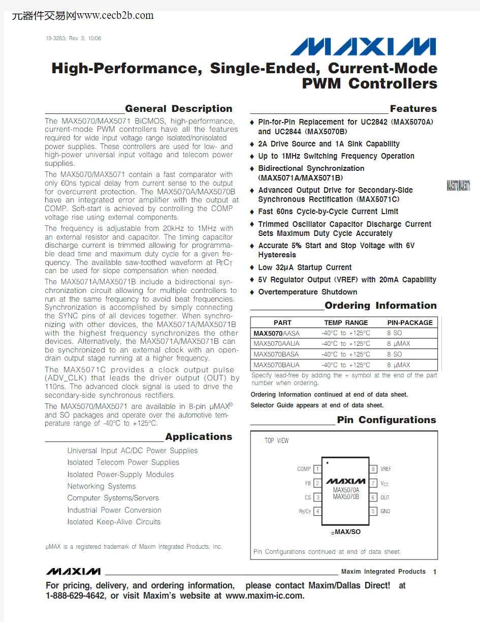
The MAX5070/MAX5071 are available in 8-pin μMAX ?and SO packages and operate over the automotive tem-perature range of -40°C to +125°C.
Applications
Universal Input AC/DC Power Supplies Isolated Telecom Power Supplies Isolated Power-Supply Modules Networking Systems Computer Systems/Servers Industrial Power Conversion Isolated Keep-Alive Circuits
Features
?Pin-for-Pin Replacement for UC2842 (MAX5070A)and UC2844 (MAX5070B)?2A Drive Source and 1A Sink Capability ?Up to 1MHz Switching Frequency Operation ?Bidirectional Synchronization (MAX5071A/MAX5071B)
?Advanced Output Drive for Secondary-Side Synchronous Rectification (MAX5071C)?Fast 60ns Cycle-by-Cycle Current Limit
?Trimmed Oscillator Capacitor Discharge Current Sets Maximum Duty Cycle Accurately ?Accurate 5% Start and Stop Voltage with 6V Hysteresis ? Low 32μA Startup Current
?5V Regulator Output (VREF) with 20mA Capability ?Overtemperature Shutdown
MAX5070/MAX5071
High-Performance, Single-Ended, Current-Mode
PWM Controllers
________________________________________________________________Maxim Integrated Products
1
Pin Configurations
19-3283; Rev 3; 10/06
For pricing, delivery, and ordering information,please contact Maxim/Dallas Direct!at 1-888-629-4642, or visit Maxim’s website at https://www.doczj.com/doc/7d8412433.html,.
Ordering Information continued at end of data sheet.Selector Guide appears at end of data sheet.
μMAX is a registered trademark of Maxim Integrated Products, Inc.
M A X 5070/M A X 5071
PWM Controllers 2_______________________________________________________________________________________
ABSOLUTE MAXIMUM RATINGS
ELECTRICAL CHARACTERISTICS
(V CC = +15V, R T = 10k ?, C T = 3.3nF, V VREF = OPEN, C VREF = 0.1μF, COMP = OPEN, V FB = 2V, CS = GND, T A = -40°C to +85°C ,unless otherwise noted.) (Note 1)
Stresses beyond those listed under “Absolute Maximum Ratings” may cause permanent damage to the device. These are stress ratings only, and functional operation of the device at these or any other conditions beyond those indicated in the operational sections of the specifications is not implied. Exposure to absolute maximum rating conditions for extended periods may affect device reliability.
V CC (Low-Impedance Source) to GND..................-0.3V to +30V V CC (I CC < 30mA).....................................................Self Limiting OUT to GND...............................................-0.3V to (V CC + 0.3V)OUT Current.............................................................±1A for 10μs FB, SYNC, COMP, CS, R T /C T , VREF to GND...........-0.3V to +6V COMP Sink Current (MAX5070)..........................................10mA
Continuous Power Dissipation (T A = +70°C)
8-Pin μMAX (derate 4.5mW/°C above +70°C).............362mW 8-Pin SO (derate 5.9mW/°C above +70°C)...............470.6mW Operating Temperature Range (Automotive)....-40°C to +125°C Maximum Junction Temperature.....................................+150°C Storage Temperature Range.............................-65°C to +150°C Lead Temperature (soldering, 10s).................................+300°C
MAX5070/MAX5071
PWM Controllers
_______________________________________________________________________________________3
ELECTRICAL CHARACTERISTICS (continued)
(V
= +15V, R = 10k ?, C = 3.3nF, V = OPEN, C = 0.1μF, COMP = OPEN, V = 2V, CS = GND, T = -40°C to +85°C ,
M A X 5070/M A X 5071
PWM Controllers
ELECTRICAL CHARACTERISTICS (continued)
(V CC = +15V, R T = 10k ?, C T = 3.3nF, V VREF = OPEN, C VREF = 0.1μF, COMP = OPEN, V FB = 2V, CS = GND, T A = -40°C to +85°C ,unless otherwise noted.) (Note 1)
ELECTRICAL CHARACTERISTICS
(V CC = +15V, R T = 10k ?, C T = 3.3nF, V VREF = OPEN, C VREF = 0.1μF, COMP = OPEN, V FB = 2V, CS = GND, T A = -40°C to +125°C ,unless otherwise noted.) (Note 1)
MAX5070/MAX5071
PWM Controllers
ELECTRICAL CHARACTERISTICS (continued)
M A X 5070/M A X 5071
PWM Controllers 6_______________________________________________________________________________________
ELECTRICAL CHARACTERISTICS (continued)
Note 1:All devices are 100% tested at +25°C. All limits over temperature are guaranteed by design, not production tested.Note 2:Guaranteed by design, not production tested.
Note 3:Parameter measured at trip point of latch with V FB = 0V (MAX5070A/MAX5070B only).Note 4:Gain is defined as A = ?V COMP /?V CS , 0 ≤V CS ≤0.8V.
Note 5:
Output Frequency equals oscillator frequency for MAX5070A/MAX5071A. Output frequency is one-half oscillator frequency for MAX5070B/MAX5071B/MAX5071C.
BOOTSTRAP UVLO vs. TEMPERATURE
TEMPERATURE (°C)
V C C (V )
110956580-105203550-25678910111213141516175
-40125
STARTUP CURRENT vs. TEMPERATURE
M A X 5070 t o c 02
TEMPERATURE (°C)
S T A R T U P C U R R E N T (μA )
110956580
-105203550-2529303132333435363738394028
-40125
2.0
2.55.5
3.53.0
4.04.5
5.0
6.0-40-10520-253550958011065125
OPERATING SUPPLY CURRENT (I CC )vs. TEMPERATURE AFTER STARTUP
(f OSC = f SW = 250kHz)
TEMPERATURE (°C)
S U P P L Y C U R R E N T (m A )
Typical Operating Characteristics
(V CC = 15V, T A = +25°C, unless otherwise noted.)
MAX5070/MAX5071
PWM Controllers
_______________________________________________________________________________________7
REFERENCE VOLTAGE (VREF)
vs. TEMPERATURE
TEMPERATURE (°C)
V V R E F (V )
110956580-105203550-25-40125
4.64.74.84.9
5.05.15.25.35.45.54.5
REFERENCE VOLTAGE (VREF)vs. REFERENCE LOAD CURRENT
M A X 5070 t o c 05
I REF (mA)
V V R E F (V )
45
30
15
4.804.854.904.95
5.005.055.105.155.205.254.75
REFERENCE VOLTAGE (VREF)
vs. V CC VOLTAGE
V CC (V)
V V R E F (V )
24
22
20
1816
14
12
4.995
5.000
5.0055.010
4.990
10
26
OSCILLATOR FREQUENCY (f OSC )
vs. TEMPERATURE
TEMPERATURE (°C)
O S C I L L A T O R F R E Q U E N C Y (k H z )
110956580-105203550-25-40125
460470480490500510520530540550450
OSCILLATOR R T /C T DISCHARGE CURRENT
vs. TEMPERATURE
TEMPERATURE (°C)
R T /C T D I S C H A R G E C U R R E N T (m A )
110956580-105203550-258.058.108.158.208.258.308.358.408.458.508.558.60
8.00
-40125
MAXIMUM DUTY CYCLE vs. TEMPERATURE
TEMPERATURE (°C)
D U T Y C Y C L
E (%)
110956580-105203550-25-40125
1020304050
607080901000
MAX5070A/MAX5071A
MAXIMUM DUTY CYCLE vs. FREQUENCY
OSCILLATOR FREQUENCY (kHz)
D U T Y C Y C L
E (%)
1200
160030201040506070809010000
400
800
2000CURRENT-SENSE (CS) TRIP THRESHOLD
vs. TEMPERATURE
M A X 5070 t o c 11
TEMPERATURE (°C)
C S T H R E S H O L
D (V )
110956580-105203550-25-40125
0.920.940.960.981.001.021.041.061.081.10
0.90
Typical Operating Characteristics (continued)
(V CC = 15V, T A = +25°C, unless otherwise noted.)
M A X 5070/M A X 5071
PWM Controllers 8_______________________________________________________________________________________
Typical Operating Characteristics (continued)
(V CC = 15V, T A = +25°C, unless otherwise noted.)
TIMING RESISTANCE (R T )vs. OSCILLATOR FREQUENCY
FREQUENCY (Hz)
R T R E S I S T A N C E (k ?)
1M
100k
1
10
100
1000
0.1
10k
10M
OUT IMPEDANCE vs. TEMPERATURE
(R DS_ON PMOS DRIVER)
TEMPERATURE (°C)
R D S _O N (?)
110956580-105203550-252.22.42.62.83.03.23.4
3.63.8
4.04.24.44.64.8
5.02.0
-40125
OUT IMPEDANCE vs. TEMPERATURE
(R DS_ON NMOS DRIVER)
TEMPERATURE (°C)
R D S _O N (?)
110956580-105203550-253.54.04.55.05.56.06.57.07.58.08.59.03.0
-40125
PROPAGATION DELAY FROM CURRENT-LIMIT COMPARATOR TO OUT vs. TEMPERATURE
M A X 5070 t o c 15
TEMPERATURE (°C)
P R O P A G A T I
O N D E L A Y (n s )
110956580-105203550-25-40125
10203040506070
80901000
ERROR-AMPLIFIER OPEN-LOOP GAIN
AND PHASE vs. FREQUENCY
FREQUENCY (Hz)
G A I N (d B )
1M 100k 1k 10k 101001
20406080100120140-200.01
100M
10M -165
-140-115-90-65-40-15
10-190
P H A S E (D E G R E E S )
COMP VOLTAGE LEVEL TO TURN OFF DEVICE
vs. TEMPERATURE
TEMPERATURE (°C)
V C O M P (V )
110956580-105203550-25-40125
1.61.71.81.9
2.0 2.12.22.3
2.42.5
1.5
ADV_CLK RISING EDGE TO OUT RISING EDGE PROPAGATION DELAY vs. TEMPERATURE
TEMPERATURE (°C)
P R O P A G A T I O N D E L A Y (n s )
110956580-105203550-259294969810010210410610811011211490
-40125
ADV_CLK AND OUT WAVEFORMS
V CC = 15V MAX5071C
OUT 10V/div
10k ? LOAD
ADV_CLK 5V/div
20ns/div
MAX5070/MAX5071
PWM Controllers
_______________________________________________________________________________________9
OUT SOURCE AND SINK CURRENTS
V CC = 15V
I OUT 2A/div
V OUT 10V/div
20Ons/div C OUT = 10nF
2
435897610202203204205201206207208209201020
SUPPLY CURRENT (I CC )
vs. OSCILLATOR FREQUENCY (C T = 100pF)
FREQUENCY (kHz)
S U P P L Y C U R R E N T (m A )
MAX5070A/MAX5071A MAXIMUM DUTY CYCLE vs. R T
R T (?)
D U T Y C Y C L
E (%)
10k 1k
30405060708090100
20100
100k
Typical Operating Characteristics (continued)
(V CC = 15V, T A = +25°C, unless otherwise noted.)
Pin Descriptions
M A X 5070/M A X 5071
PWM Controllers 10______________________________________________________________________________________
Pin Descriptions (continued)
MAX5071A/MAX5071B/MAX5071C
Detailed Description
The MAX5070/MAX5071 current-mode PWM controllers are designed for use as the control and regulation core of flyback or forward topology switching power supplies.These devices incorporate an integrated low-side driver,adjustable oscillator, error amplifier (MAX5070A/MAX5070B only), current-sense amplifier, 5V reference,and external synchronization capability (MAX5071A/MAX5071B only). An internal +26.5V current-limited V CC clamp prevents overvoltage during startup.
Five different versions of the MAX5070/MAX5071 are available. The MAX5070A/MAX5070B are the standard
versions with a feedback input (FB) and internal error amplifier. The MAX5071A/MAX5071B include bidirection-al synchronization (SYNC). This enables multiple MAX5071A/MAX5071Bs to be connected and synchro-nized to the device with the highest frequency. The MAX5071C includes an ADV_CLK output, which pre-cedes the MAX5071C’s drive output (OUT) by 110ns.Figures 1, 2, and 3 show the internal functional diagrams of the MAX5070A/MAX5070B, MAX5071A/MAX5071B,and MAX5071C, respectively. The MAX5070A/MAX5071A are capable of 100% maximum duty cycle.The MAX5070B/MAX5071B/MAX5071C are designed to limit the maximum duty cycle to 50%.
MAX5070/MAX5071
PWM Controllers
______________________________________________________________________________________11
Figure 1. MAX5070A/MAX5070B Functional Diagram
M A X 5070/M A X 5071
Current-Mode Control Loop
The advantages of current-mode control over voltage-mode control are twofold. First, there is the feed-forward characteristic brought on by the controller’s ability to adjust for variations in the input voltage on a cycle-by-cycle basis. Secondly, the stability requirements of the current-mode controller are reduced to that of a single-pole system unlike the double pole in the voltage-mode control scheme.The MAX5070/MAX5071 use a current-mode control loop where the output of the error amplifier is compared to the current-sense voltage (V CS ). When the current-sense sig-nal is lower than the noninverting input of the PWM com-parator, the output of the CPWM comparator is low and the switch is turned on at each clock pulse. When the current-sense signal is higher than the inverting input of the CPWM, the output of the CPWM comparator is high and the switch is turned off.
PWM Controllers 12______________________________________________________________________________________
Figure 2. MAX5071A/MAX5071B Functional Diagram
V CC and Startup
In normal operation, V CC is derived from a tertiary wind-ing of the transformer. However, at startup there is no energy delivered through the transformer, thus a resistor must be connected from V CC to the input power source (see R ST and C ST in Figures 5 to 8). During startup, C ST charges up through R ST . The 5V reference generator,comparator, error amplifier, oscillator, and drive circuit remain off during UVLO to reduce startup current below 65μA. When V CC reaches the undervoltage-lockout threshold of 16V, the output driver begins to switch and the tertiary winding will supply power to V CC . V CC has an internal 26.5V current-limited clamp at its input to protect the device from overvoltage during startup.
Size the startup resistor, R ST , to supply both the maxi-mum startup bias (I START ) of the device (65μA max)and the charging current for C ST . The startup capacitor C ST must charge to 16V within the desired time period t ST (for example, 500ms). The size of the startup capacitor depends on:
1)IC operating supply current at a programmed oscilla-tor frequency (f OSC ).
2)The time required for the bias voltage, derived from
a bias winding, to go from 0 to 11V.3)The MOSFET total gate charge.
4)The operating frequency of the converter (f SW ).
MAX5070/MAX5071
PWM Controllers
______________________________________________________________________________________13
Figure 3. MAX5071C Functional Diagram
M A X 5070/M A X 5071
To calculate the capacitance required, use the following formula:
where:
I G = Q G f SW
I CC is the MAX5070/MAX5071s’ maximum internal sup-ply current after startup (see the Typical Operating Characteristics to find the I IN at a given f OSC ). Q G is the total gate charge for the MOSFET, f SW is the converter switching frequency, V HYST is the bootstrap UVLO hys-teresis (6V), and t SS is the soft-start time, which is set by external circuitry.
Size the resistor R ST according to the desired startup time period, t ST , for the calculated C ST . Use the follow-ing equations to calculate the average charging current (I CST ) and the startup resistor (R ST ).
Where V INMIN is the minimum input supply voltage for the application (36V for telecom), V SUVR is the boot-strap UVLO wake-up level (16V), and I START is the V IN supply current at startup (65μA, max). Choose a higher value for R ST than the one calculated above if longer startup times can be tolerated in order to minimize power loss in R ST .
The above startup method is applicable to circuits where the tertiary winding has the same phase as the output windings. Thus, the voltage on the tertiary winding at any given time is proportional to the output voltage and goes through the same soft-start period as the output voltage.The minimum discharge time of C ST from 16V to 10V must be greater than the soft-start time (t SS ).
Undervoltage Lockout (UVLO)
The minimum turn-on supply voltage for the MAX5070/MAX5071 is 16V. Once V CC reaches 16V, the reference powers up. There is 6V of hysteresis from the minimum turn-on voltage to the UVLO threshold. Once V CC reaches 16V, the MAX5070/MAX5071 will operate with V CC down to 10V. Once V CC goes below 10V the device is in UVLO. When in UVLO, the quiescent sup-ply current into V CC falls back to 37μA (typ), and OUT and VREF are pulled low.
MOSFET Driver
OUT drives an external n-channel MOSFET and swings from GND to V CC . Ensure that V CC remains below the absolute maximum V GS rating of the external MOSFET.OUT is a push-pull output with the on-resistance of the PMOS typically 3.5?and the on-resistance of the NMOS typically 4.5?. The driver can source 2A typically and sink 1A typically. This allows for the MAX5070/MAX5071to quickly turn on and off high gate-charge MOSFETs.Bypass V CC with one or more 0.1μF ceramic capacitors to GND, placed close to the MAX5070/MAX5071. The average current sourced to drive the external MOSFET depends on the total gate charge (Q G ) and operating frequency of the converter. The power dissipation in the MAX5070/MAX5071 is a function of the average output drive current (I DRIVE ). Use the following equation to cal-culate the power dissipation in the device due to I DRIVE :
I DRIVE = Q G x f SW
PD = (I DRIVE + I CC ) x V CC
where I CC is the operating supply current. See the Typical Operating Characteristics for the operating supply current at a given frequency.
Error Amplifier (MAX5070A/MAX5070B)
The MAX5070 includes an internal error amplifier. The inverting input is at FB and the noninverting input is inter-nally connected to a 2.5V reference. The internal error amplifier is useful for nonisolated converter design (see Figure 6) and isolated design with primary-side regulation through a bias winding (see Figure 5). I n the case of a nonisolated power supply, the output voltage will be:
where R1 and R2 are from Figure
6.
PWM Controllers 14______________________________________________________________________________________
MAX5071A/MAX5071B/MAX5071C
Feedback The MAX5071A/MAX5071B/MAX5071C are designed to be used with either an external error amplifier when designed into a nonisolated converter or an error ampli-fier and optocoupler when designed into an isolated power supply. The COMP input is level-shifted and connected to the inverting terminal of the PWM com-parator (CPWM). Connect the COMP pin to the output of the external error amplifier for nonisolated design. Pull COMP high externally to at least 5V (or VREF) and connect the optocoupler transistor as shown in Figures 7 and 8. COMP can be used for soft-start and also as a shutdown. See the Typical Operating Characteristics to find the turn-off COMP voltage at different tempera-tures. If the maximum external COMP voltage is below 4.9V, it may reduce the PWM current-limit threshold below 1V. Use the following equation to calculate mini-mum COMP voltage (V COMP) required for a guaranteed peak primary current (I P-P):
V COMP= (3 x I P-P x R CS) + 1.95V
where R CS is a current-sense resistor.
Oscillator The oscillator frequency is adjusted by adding an external capacitor and resistor at R T/C T(see R T and C T in the Typical Application Circuits). R T is connected from R T/C T to the 5V reference (VREF) and C T is con-nected from R T/C T to GND. VREF charges C T through R T until its voltage reaches 2.8V. C T then discharges through an 8.3mA internal current sink until C T’s voltage reaches 1.1V, at which time C T is allowed to charge through R T again. The oscillator’s period will be the sum of the charge and discharge times of C T. Calculate the charge time as:
t C= 0.57 x R T x C T
The discharge time is then:
The oscillator frequency will then be:
For the MAX5070A/MAX5071A, the converter output switching frequency (f SW) is the same as the oscillator frequency (f OSC). For the MAX5070B/MAX5071B/ MAX5071C, the output switching frequency is 1/2 the oscillator frequency.
Reference Output VREF is a 5V reference output that can source 20mA. Bypass VREF to GND with a 0.1μF capacitor.
Current Limit The MAX5070/MAX5071 include a fast current-limit com-parator to terminate the ON cycle during an overload or a fault condition. The current-sense resistor (R CS), connect-ed between the source of the MOSFET and GND, sets the current limit. The CS input has a voltage trip level (V CS) of 1V. Use the following equation to calculate R CS:
P-P
the MOSFET. When the voltage produced by this current (through the current-sense resistor) exceeds the current-limit comparator threshold, the MOSFET driver (OUT) will turn the switch off within 60ns. In most cases, a small RC filter is required to filter out the leading-edge spike on the sense waveform. Set the time constant of the RC filter at 50ns. Use a current transformer to limit the losses in the current-sense resistor and achieve higher efficiency
especially at low input-voltage operation.
Synchronization (MAX5071A/MAX5071B)
SYNC
SYNC is a bidirectional input/output that outputs a syn-
chronizing pulse and accepts a synchronizing pulse
from other MAX5071A/MAX5071Bs (see Figures 7 and
9). As an output, SYNC is an open-drain p-channel
MOSFET driven from the internal oscillator and requires
an external pulldown resistor (R SYNC
) from between
500?and 5k?. As an input, SYNC accepts the output
pulses from other MAX5071A/MAX5071Bs.
Synchronize multiple MAX5071A/MAX5071Bs by con-
necting their SYNC pins together. All devices connected
together will synchronize to the one operating at the
highest frequency. The rising edge of SYNC will precede
the rising edge of OUT by approximately the discharge
time (t D) of the oscillator (see the Oscillator section). The
pulse width of the SYNC output is equal to the time
required to discharge the stray capacitance at SYNC
through R SYNC plus the C T discharge time t D. Adjust
R T/C T such that the minimum discharge time t D is 200ns.
MAX5070/MAX5071
PWM Controllers
______________________________________________________________________________________15
M A X 5070/M A X 5071
Advance Clock Output (ADV_CLK) (MAX5071C)ADV_CLK is an advanced pulse output provided to facilitate the easy implementation of secondary-side synchronous rectification using the MAX5071C. The ADV_CLK pulse width is 85ns (typically) with its rising edge leading the rising edge of OUT by 110ns. Use this leading pulse to turn off the secondary-side syn-chronous-rectifier MOSFET (QS) before the voltage appears on the secondary (see Figure 8). Turning off the secondary-side synchronous MOSFET earlier avoids the shorting of the secondary in the forward converter. The ADV_CLK pulse can be propagated to the secondary side using a pulse transformer or high-speed optocoupler. The 85ns pulse, with 3V drive volt-age (10mA source), significantly reduces the volt-second requirement of the pulse transformer and the advanced pulse alleviates the need for a high-speed optocoupler.
Thermal Shutdown
When the MAX5070/MAX5071s’ die temperature goes above +150°C, the thermal-shutdown circuitry will shut down the 5V reference and pull OUT low.
PWM Controllers 16______________________________________________________________________________________
Typical Application Circuits
Figure 5. MAX5070A/MAX5070B Typical Application Circuit (Isolated Flyback with Primary-Side Regulation)
MAX5070/MAX5071
PWM Controllers
______________________________________________________________________________________
17
Typical Application Circuits (continued)
Figure 6. MAX5070A/MAX5070B Typical Application Circuit (Non-Isolated Flyback)
Figure 7. MAX5071A/MAX5071B Typical Application Circuit (Isolated Flyback)
M A X 5070/M A X 5071
PWM Controllers 18______________________________________________________________________________________
Typical Application Circuits (continued)
Figure 8. MAX5071C Typical Application Circuit (Isolated Forward with Secondary-Side Synchronous Rectification)
MAX5070/MAX5071
PWM Controllers
______________________________________________________________________________________19
Figure 9. Synchronization of MAX5071s
M A X 5070/M A X 5071
PWM Controllers 20______________________________________________________________________________________
Chip Information
TRANSISTOR COUNT:1987PROCESS:BiCMOS
Ordering Information (continued)
Pin Configurations (continued)
Selector Guide
Specify lead-free by adding the + symbol at the end of the part number when ordering.