? 2000 Fairchild Semiconductor Corporation DS005355
https://www.doczj.com/doc/7a5269655.html,
August 1984
Revised January 2000
MM74HC4066 Quad Analog Switch
MM74HC4066
Quad Analog Switch
General Description
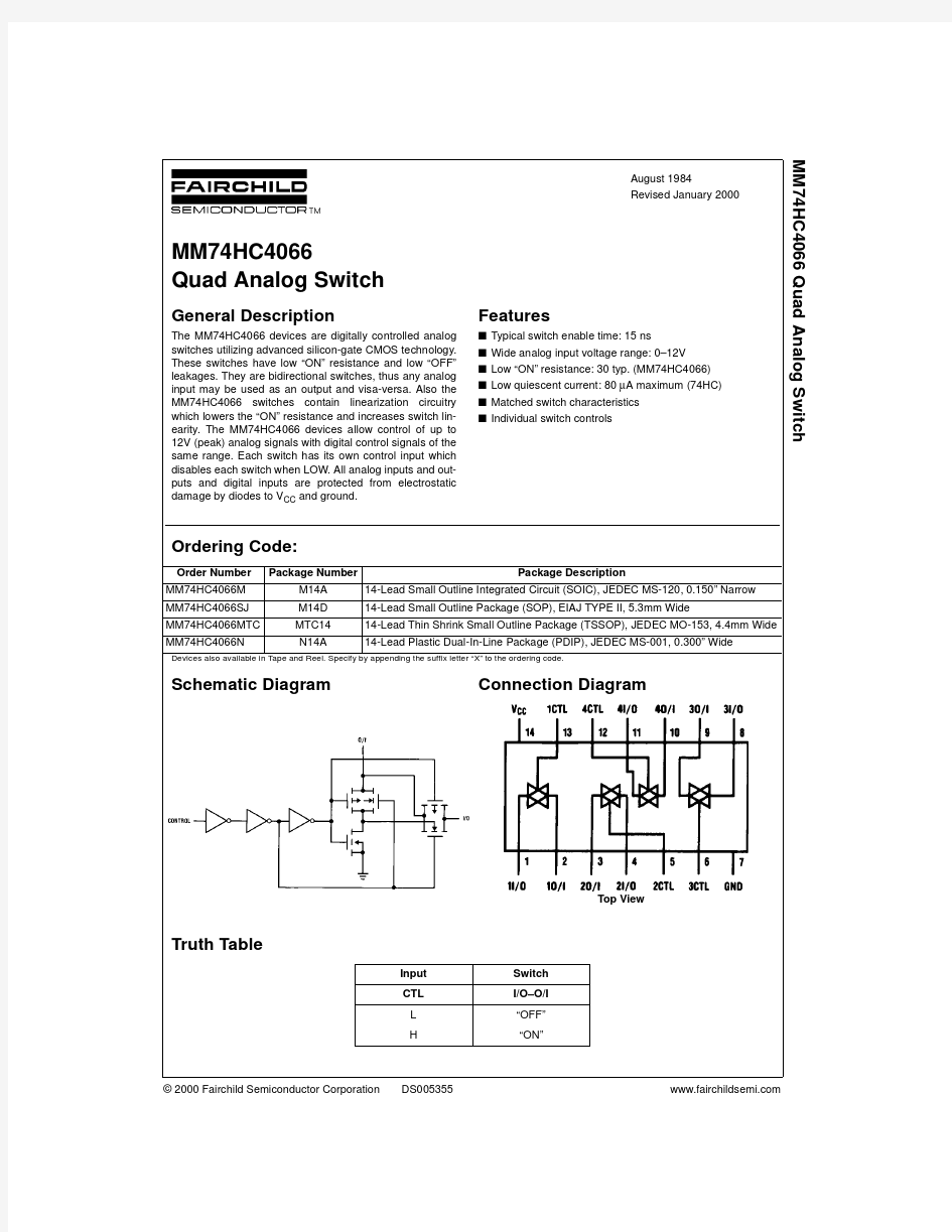
The MM74HC4066 devices are digitally controlled analog switches utilizing advanced silicon-gate CMOS technology.These switches have low “ON” resistance and low “OFF”leakages. They are bidirectional switches, thus any analog input may be used as an output and visa-versa. Also the MM74HC4066 switches contain linearization circuitry which lowers the “ON” resistance and increases switch lin-earity. The MM74HC4066 devices allow control of up to 12V (peak) analog signals with digital control signals of the same range. Each switch has its own control input which disables each switch when LOW. All analog inputs and out-puts and digital inputs are protected from electrostatic damage by diodes to V CC and ground.Features
s Typical switch enable time: 15 ns s Wide analog input voltage range: 0–12V s Low “ON” resistance: 30 typ. (MM74HC4066)s Low quiescent current: 80 μA maximum (74HC)s Matched switch characteristics s Individual switch controls
Ordering Code:
Devices also available in Tape and Reel. Specify by appending the suffix letter “X” to the ordering code.
Schematic Diagram Connection Diagram
Top View
Truth Table
Order Number Package Number
Package Description
MM74HC4066M M14A 14-Lead Small Outline Integrated Circuit (SOIC), JEDEC MS-120, 0.150” Narrow MM74HC4066SJ M14D 14-Lead Small Outline Package (SOP), EIAJ TYPE II, 5.3mm Wide
MM74HC4066MTC MTC1414-Lead Thin Shrink Small Outline Package (TSSOP), JEDEC MO-153, 4.4mm Wide MM74HC4066N
N14A
14-Lead Plastic Dual-In-Line Package (PDIP), JEDEC MS-001, 0.300” Wide
Input Switch CTL I/O–O/I L “OFF”H
“ON”
https://www.doczj.com/doc/7a5269655.html, 2
M M 74H C 4066
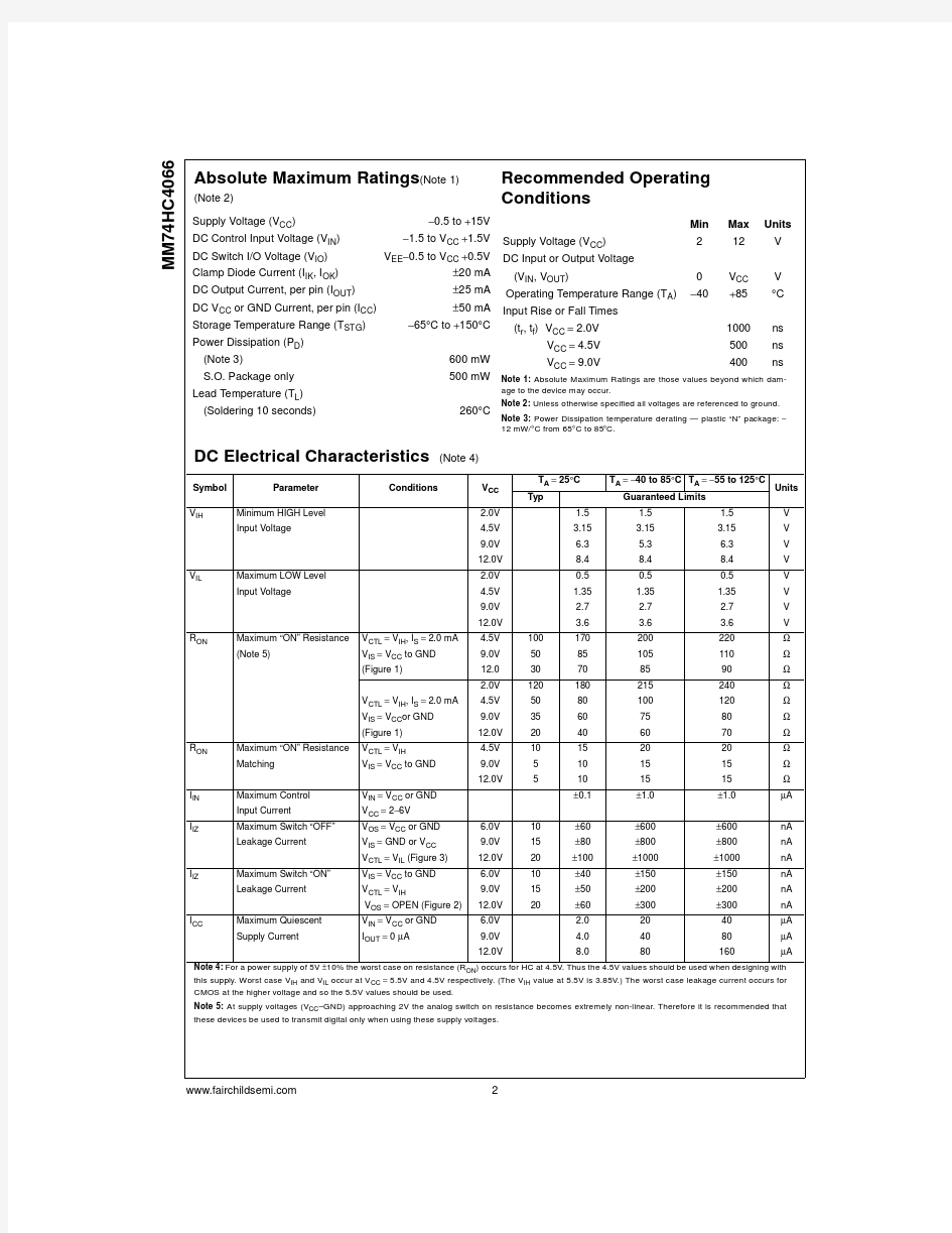
Absolute Maximum Ratings (Note 1)
(Note 2)
Recommended Operating Conditions
Note 1: Absolute Maximum Ratings are those values beyond which dam-age to the device may occur.
Note 2: Unless otherwise specified all voltages are referenced to ground.Note 3: Power Dissipation temperature derating — plastic “N” package: ?12 mW/°C from 65°C to 85°C.
DC Electrical Characteristics (Note 4)
Note 4: For a power supply of 5V ±10% the worst case on resistance (R ON ) occurs for HC at 4.5V. Thus the 4.5V values should be used when designing with this supply. Worst case V IH and V IL occur at V CC = 5.5V and 4.5V respectively. (The V IH value at 5.5V is 3.85V.) The worst case leakage current occurs for CMOS at the higher voltage and so the 5.5V values should be used.
Note 5: At supply voltages (V CC –GND) approaching 2V the analog switch on resistance becomes extremely non-linear. Therefore it is recommended that these devices be used to transmit digital only when using these supply voltages.
Supply Voltage (V CC )
?0.5 to +15V DC Control Input Voltage (V IN )?1.5 to V CC +1.5V DC Switch I/O Voltage (V IO )V EE ?0.5 to V CC +0.5V
Clamp Diode Current (I IK , I OK )±20 mA DC Output Current, per pin (I OUT )±25 mA DC V CC or GND Current, per pin (I CC )±50 mA
Storage Temperature Range (T STG )?65°C to +150°C
Power Dissipation (P D )(Note 3)
600 mW S.O. Package only 500 mW Lead T emperature (T L )(Soldering 10 seconds)
260°C Min
Max Units Supply Voltage (V CC )2
12
V
DC Input or Output Voltage (V IN , V OUT )
0V CC V Operating Temperature Range (T A )?40
+85
°C
Input Rise or Fall Times (t r , t f ) V CC = 2.0V
1000ns V CC = 4.5V 500ns V CC = 9.0V
400
ns
Symbol Parameter
Conditions
V CC T A = 25°C T A = ?40 to 85°C T A = ?55 to 125°C Units Typ
Guaranteed Limits
V IH
Minimum HIGH Level 2.0V 1.5 1.5 1.5V Input Voltage
4.5V 3.15 3.15 3.15V 9.0V 6.3
5.3
6.3V 12.0V
8.48.48.4V V IL
Maximum LOW Level 2.0V 0.50.50.5V Input Voltage
4.5V 1.35 1.35 1.35V 9.0V 2.7 2.7 2.7V 12.0V
3.6 3.6 3.6V R ON
Maximum “ON” Resistance V CTL = V IH , I S = 2.0 mA 4.5V 100170200220?(Note 5)
V IS = V CC to GND 9.0V 5085105110?(Figure 1)
12.030708590?2.0V 120180215240?V CTL = V IH , I S = 2.0 mA 4.5V 5080100120?V IS = V CC or GND 9.0V 35607580?(Figure 1)
12.0V 20406070?R ON
Maximum “ON” Resistance V CTL = V IH 4.5V 10152020?Matching
V IS = V CC to GND 9.0V 5101515?12.0V
5
101515?I IN Maximum Control V IN = V CC or GND ±0.1
±1.0
±1.0
μA
Input Current
V CC = 2?6V I IZ
Maximum Switch “OFF”V OS = V CC or GND 6.0V 10±60±600±600nA Leakage Current
V IS = GND or V CC 9.0V 15±80±800±800nA V CTL = V IL (Figure 3)12.0V 20±100±1000±1000nA I IZ
Maximum Switch “ON”V IS = V CC to GND 6.0V 10±40±150±150nA Leakage Current
V CTL = V IH
9.0V 15±50±200±200nA V OS = OPEN (Figure 2)12.0V 20
±60±300±300nA I CC
Maximum Quiescent V IN = V CC or GND 6.0V 2.02040μA Supply Current
I OUT = 0 μA
9.0V 4.04080μA 12.0V
8.0
80
160
μA
https://www.doczj.com/doc/7a5269655.html,
MM74HC4066
AC Electrical Characteristics
V CC = 2.0V ?6.0V V EE = 0V ?12V, C L = 50 pF (unless otherwise specified)Note 6: Adjust 0 dBm for F = 1 kHz (Null R L /R ON Attenuation).Note 7: V IS is centered at V CC /2.Note 8: Adjust input for 0 dBm.
Symbol
Parameter
Conditions
V CC T A = 25°C T A = ?40 to 85°C T A = ?55 to 125°C
Units Typ Guaranteed Limits
t PHL , t PLH Maximum Propagation
2.0V 25503075ns Delay Switch In to Out
4.5V 5101315ns 9.0V 481012ns 12.0V
371113ns t PZL , t PZH Maximum Switch Turn
R L = 1 k ?
2.0V 30100125150ns “ON” Delay
4.5V 12202530ns 9.0V 6121518ns 12.0V
5101315ns t PHZ , t PLZ Maximum Switch Turn
R L = 1 k ?
2.0V 60168210252ns “OFF” Delay
4.5V 25364554ns 9.0V 20324048ns 12.0V
1530
38
45
f MAX
Minimum Frequency R L = 600?
4.5V 40MHz Response (Figure 7)V IS = 2 V PP at (V CC /2)9.0V
100
MHz
20 log (V O /V I ) = ?3 dB (Note 6) (Note 7)Crosstalk Between R L = 600?, F = 1 MHz any Two Switches (Note 7) (Note 8) 4.5V ?52dB (Figure 8)
9.0V ?50dB Peak Control to Switch R L = 600?, F = 1 MHz 4.5V 100mV Feedthrough Noise (Figure 9)C L = 50 pF
9.0V
250
mV
Switch OFF Signal R L = 600?, F = 1 MHz Feedthrough V (CT)V IL
Isolation (Note 7) (Note 8) 4.5V ?42dB (Figure 10)
9.0V
?44
dB
THD
Total Harmonic R L = 10 k ?, C L = 50 pF ,Distortion F = 1 kHz (Figure 11)
V IS = 4 V PP 4.5V .013%V IS = 8 V PP
9.0V
.008%C IN Maximum Control 510
10
10
pF Input Capacitance C IN Maximum Switch 20
pF Input Capacitance C IN Maximum Feedthrough V CTL = GND 0.5pF Capacitance C PD
Power Dissipation 15
pF
Capacitance
https://www.doczj.com/doc/7a5269655.html, 4
M M 74H C 4066
AC Test Circuits and Switching Time Waveforms
FIGURE 1. “ON” Resistance
FIGURE 2. “ON” Channel Leakage Current
FIGURE 3. “OFF” Channel Leakage Current
FIGURE 4. t PHL , t PLH Propagation Delay Time Signal Input to Signal Output
FIGURE 5. t PZL , t PLZ Propagation Delay Time Control to Signal Output
FIGURE 6. t PZH , t PHZ Propagation Delay Time Control to Signal Output
5
https://www.doczj.com/doc/7a5269655.html,
MM74HC4066
AC Test Circuits and Switching Time Waveforms (Continued)
FIGURE 7. Frequency Response
FIGURE 8. Crosstalk: Control Input to Signal Output
FIGURE 9. Crosstalk Between Any Two Switches
FIGURE 10. Switch OFF Signal Feedthrough Isolation
FIGURE 11. Sinewave Distortion
https://www.doczj.com/doc/7a5269655.html, 6
M M 74H C 4066
Typical Performance Characteristics
Typical “ON” Resistance
Typical Crosstalk Between
Any Two Switches
Typical Frequency Response
Special Considerations
In certain applications the external load-resistor current may include both V CC and signal line components. T o avoid drawing V CC current when switch current flows into
the analog switch input pins, the voltage drop across the switch must not exceed 0.6V (calculated from the ON resis-tance).
https://www.doczj.com/doc/7a5269655.html, MM74HC4066
Physical Dimensions inches (millimeters) unless otherwise noted
14-Lead Small Outline Integrated Circuit (SOIC), JEDEC MS-120, 0.150” Narrow
Package Number M14A
https://www.doczj.com/doc/7a5269655.html, 8
M M 74H C 4066
Physical Dimensions
inches (millimeters) unless otherwise noted (Continued)
14-Lead Small Outline Package (SOP), EIAJ TYPE II, 5.3mm Wide
Package Number M14D
https://www.doczj.com/doc/7a5269655.html, MM74HC4066
Physical Dimensions inches (millimeters) unless otherwise noted (Continued)
14-Lead Thin Shrink Small Outline Package (TSSOP), JEDEC MO-153, 4.4mm Wide
Package Number MTC14
https://www.doczj.com/doc/7a5269655.html,
10
M M 74H C 4066 Q u a d A n a l o g S w i t c h
Physical Dimensions inches (millimeters) unless otherwise noted (Continued)
14-Lead Plastic Dual-In-Line Package (PDIP), JEDEC MS-001, 0.300” Wide
Package Number N14A
Fairchild does not assume any responsibility for use of any circuitry described, no circuit patent licenses are implied and Fairchild reserves the right at any time without notice to change said circuitry and specifications.LIFE SUPPORT POLICY
FAIRCHILD’S PRODUCTS ARE NOT AUTHORIZED FOR USE AS CRITICAL COMPONENTS IN LIFE SUPPORT DEVICES OR SYSTEMS WITHOUT THE EXPRESS WRITTEN APPROVAL OF THE PRESIDENT OF FAIRCHILD SEMICONDUCTOR CORPORATION. As used herein:1.Life support devices or systems are devices or systems which, (a) are intended for surgical implant into the body, or (b) support or sustain life, and (c) whose failure to perform when properly used in accordance with instructions for use provided in the labeling, can be rea-sonably expected to result in a significant injury to the user. 2. A critical component in any component of a life support device or system whose failure to perform can be rea-sonably expected to cause the failure of the life support device or system, or to affect its safety or effectiveness.
https://www.doczj.com/doc/7a5269655.html,