
HD74LS48
BCD-to-Seven-Segment Decoder / Driver (Internal Pull-up outputs)
REJ03D0411–0300
Rev.3.00 Jul.22.2005
HD74LS48 features active high outputs for driving lamp buffers. This circuit has full ripple blanking input / output controls and a lamp test input. Display patterns for BCD input counts above 9 are unique symbols to authenticate input conditions. This circuit incorporates automatic leading and / or trailing-edge zero-blanking control (RBI and RBO). Lamp test (LT) of these types may be performed at any time when the BI / RBO node is at a high level. It contains an overriding blanking input (BI) which can be used to control the lamp intensity be pulsing or to inhibit the outputs. Inputs and outputs are entirely compatible for use with TTL or DTL logic outputs.
Features
? Ordering Information
Part Name
Package Type
Package Code (Previous Code) Package
Abbreviation
Taping Abbreviation (Quantity)
HD74LS48P DILP-16 pin PRDP0016AE-B (DP-16FV)
P —
Pin Arrangement
V CC GND
B
C Lamp
Test BI/RBO
RBI D
A f g b a c d e
15161234567148
9
10111213Outputs
Inputs
Inputs
B C D A
RBI BI/RBO LT f g d e
c b a
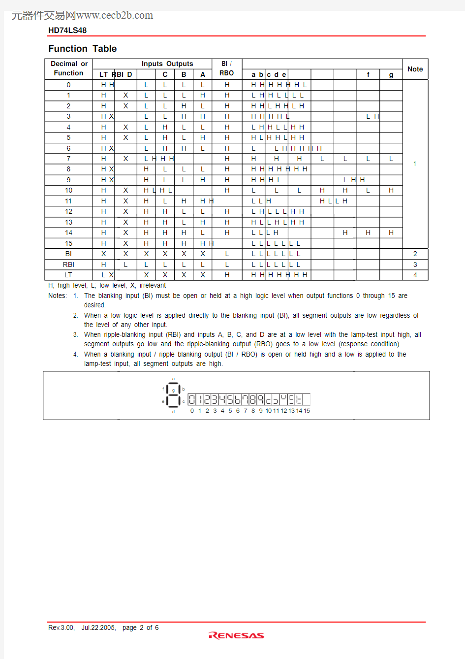
Function Table
Inputs Outputs
Decimal or Function
LT RBI D C B A BI / RBO
a b c d e f g Note
0 H H L L L L H H H H H H H L 1 H X L L L H H L H H L L L L
2 H X L L H L H H H L H H L H
3 H X L L H H H H H H H L L H
4 H X L H L L H L H H L L H H
5 H X L H L H H H L H H L H H
6 H X L H H L H L L H H H H H
7 H X L H H H H H H H L L L L
8 H X H L L L H H H H H H H H 9 H X H L L H H H H H L L H H 10 H X H L H L H L L L H H L H 11 H X H L H H H L L H H L L H 12 H X H H L L H L H L L L H H 13 H X H H L H H H L L H L H H 14 H X H H H L H L L L H H H H 15 H X H H H H H L L L L L L L 1
BI X X X X X X L L L L L L L L 2 RBI H L L L L L L L L L L L L L 3 LT
L X X X X X H H H H H H H H 4
H; high level, L; low level, X, irrelevant
Notes: 1. The blanking input (BI) must be open or held at a high logic level when output functions 0 through 15 are
desired.
2. When a low logic level is applied directly to the blanking input (BI), all segment outputs are low regardless of
the level of any other input.
3. When ripple-blanking input (RBI) and inputs A, B, C, and D are at a low level with the lamp-test input high, all
segment outputs go low and the ripple-blanking output (RBO) goes to a low level (response condition).
4. When a blanking input / ripple blanking output (BI / RBO) is open or held high and a low is applied to the
lamp-test input, all segment outputs are high.
a 5432106789101112131415
b d c
f e
g
Block Diagram
D
Blanking Input or
Ripple Blanking
Output (BI/RBO)
Lamp Test (LT)
Ripple Blanking (RBI)
Absolute Maximum Ratings
Item Symbol
Unit
Ratings
Supply voltage V CC 7 V Input voltage VI N 7 V Power dissipation P T 400 mW Storage temperature Tstg –65 to +150 °C
Note: Voltage value, unless otherwise noted, are with respect to network ground terminal.
Recommended Operating Conditions
Max
Unit
Min
Item Symbol
Typ
Supply voltage V CC 4.75 5.00 5.25 V
I OH (a to g) — — –100 μA
Output current
I OH (BI/RBO) — — –50 μA
I OL (a to g) — — 6 mA
Output current
I OL (BI/RBO) — — 3.2 mA
Operating temperature Topr -20 25 75 °C
Electrical Characteristics
(Ta = –20 to +75 °C)
Item Symbol min. typ.* max. Unit Condition
V IH 2.0 — — V
Input voltage
V IL —
— 0.8 V a to g 2.4 — — V I OH = –100 μA BI / RBO V OH
2.4 — — V I OH = –50 μA V CC = 4.75 V,
V IH = 2 V, V IL = 0.8 V — — 0.4 I OL = 2 mA
a to g — — 0.5 V
I OL = 6 mA — — 0.4 I OL = 1.6 mA
Output voltage
BI / RBO
V OL
— — 0.5 V
I OL = 3.2 mA
V CC = 4.75 V,
V IH = 2 V, V IL = 0.8 V Output current** a to g
I O –1.3 — — mA V CC = 4.75 V, V O = 0.85 V, I IH — — 20 μA V CC = 5.25 V, V I = 2.7 V
except BI
/ RBO
— — –0.4 mA V CC = 5.25 V, V I = 0.4 V
BI / RBO I IL
— — –1.2 mA V CC = 5.25 V, V I = 0.4 V Input current
except BI / RBO
I I — — 0.1 mA V CC = 5.25 V, V I = 7 V Short-circuit
output current BI / RBO
I OS –0.3 — –2 mA V CC = 5.25 V Supply current***
I CC — 25 38 mA V CC = 5.25 V
Input clamp voltage V IK — — –1.5 V V CC = 4.75 V, I IN = –18 mA Notes: * V CC = 5 V, Ta = 25°C ** Input condition as for V OH *** I CC is measured with all outputs open and inputs at 4.5 V.
Switching Characteristics
(V CC = 5 V, Ta = 25°C)
Item Symbol Input min. typ. max. Unit Condition
t PHL — — 100
Turn-on time t PLH A — — 100 ns C L = 15 pF, R L = 4 k ?
t PHL — — 100
Turn-off time t PLH RBI — — 100
ns C L = 15 pF, R L = 6 k ?
Testing Method
Test Circuit
Waveform
t PLH
t PHL
t PHL
t PLH
10%
90%1.3 V
1.3 V
1.3 V
1.3 V
1.3 V
1.3 V
10%
90%In phase output
Out of phase output
t TLH
t THL
Testing Table
Inputs Outputs
Item
RBI D C B A a b c d e f g 4.5 V GND GND GND IN OUT — — OUT OUT OUT — 4.5 V GND GND 4.5 V IN — — OUT — OUT — — 4.5 V
GND
4.5 V
4.5 V
IN
OUT
OUT
—
OUT
OUT
OUT
OUT
t PLH t PHL IN GND GND GND GND OUT OUT OUT OUT OUT OUT —
Package Dimensions
1
p
1
e b A L
A
e
c
θ
( Ni/Pd/Au plating )
https://www.doczj.com/doc/6b16297789.html, RENESAS SALES OFFICES
Refer to "https://www.doczj.com/doc/6b16297789.html,/en/network" for the latest and detailed information.
Renesas Technology America, Inc.
450 Holger Way, San Jose, CA 95134-1368, U.S.A
Tel: <1> (408) 382-7500, Fax: <1> (408) 382-7501
Renesas Technology Europe Limited
Dukes Meadow, Millboard Road, Bourne End, Buckinghamshire, SL8 5FH, U.K.
Tel: <44> (1628) 585-100, Fax: <44> (1628) 585-900
Renesas Technology Hong Kong Ltd.
7th Floor, North Tower, World Finance Centre, Harbour City, 1 Canton Road, Tsimshatsui, Kowloon, Hong Kong
Tel: <852> 2265-6688, Fax: <852> 2730-6071
Renesas Technology Taiwan Co., Ltd.
10th Floor, No.99, Fushing North Road, Taipei, Taiwan
Tel: <886> (2) 2715-2888, Fax: <886> (2) 2713-2999
Renesas Technology (Shanghai) Co., Ltd.
Unit2607 Ruijing Building, No.205 Maoming Road (S), Shanghai 200020, China
Tel: <86> (21) 6472-1001, Fax: <86> (21) 6415-2952
Renesas Technology Singapore Pte. Ltd.
1 Harbour Front Avenue, #06-10, Keppel Bay Tower, Singapore 098632
Tel: <65> 6213-0200, Fax: <65> 6278-8001
Renesas Technology Korea Co., Ltd.
Kukje Center Bldg. 18th Fl., 191, 2-ka, Hangang-ro, Yongsan-ku, Seoul 140-702, Korea
Tel: <82> 2-796-3115, Fax: <82> 2-796-2145
Renesas Technology Malaysia Sdn. Bhd.
Unit 906, Block B, Menara Amcorp, Amcorp Trade Centre, No.18, Jalan Persiaran Barat, 46050 Petaling Jaya, Selangor Darul Ehsan, Malaysia
Tel: <603> 7955-9390, Fax: <603> 7955-9510