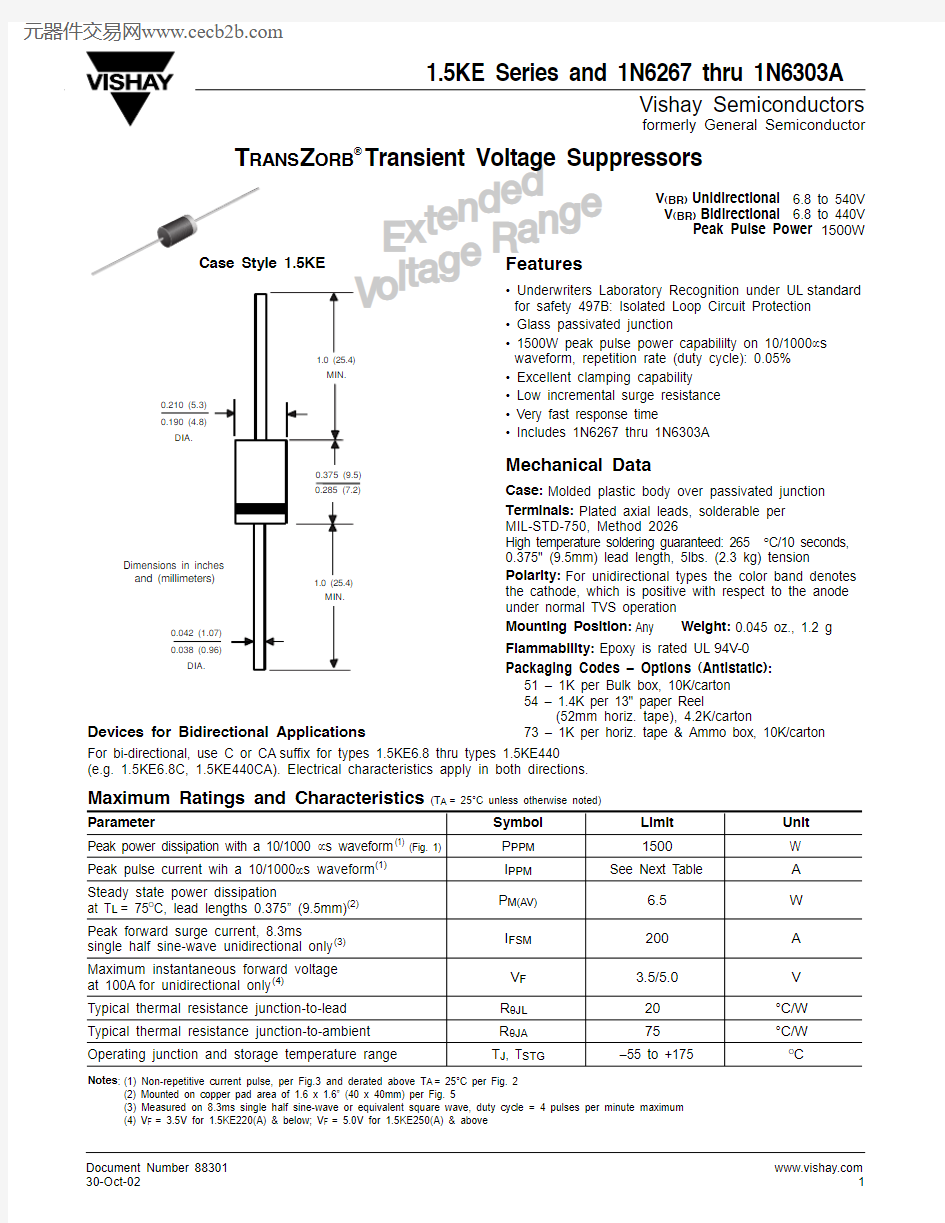
Devices for Bidirectional Applications
For bi-directional, use C or CA suffix for types 1.5KE6.8 thru types 1.5KE440 (e.g. 1.5KE6.8C, 1.5KE440CA). Electrical characteristics apply in both directions.
Maximum Ratings and Characteristics
(T A = 25°C unless otherwise noted)
Parameter
Symbol Limit Unit Peak power dissipation with a 10/1000μs waveform (1) (Fig. 1)P PPM 1500W Peak pulse current wih a 10/1000μs waveform (1)I PPM See Next Table
A Steady state power dissipation
P M(AV) 6.5W at T L = 75O C, lead lengths 0.375” (9.5mm)(2)Peak forward surge current, 8.3ms
I FSM 200A single half sine-wave unidirectional only (3)Maximum instantaneous forward voltage V F 3.5/5.0V at 100A for unidirectional only (4)
Typical thermal resistance junction-to-lead R θJL 20°C/W Typical thermal resistance junction-to-ambient R θJA 75°C/W
Operating junction and storage temperature range
T J , T STG
–55 to +175
O
C
Notes :(1) Non-repetitive current pulse, per Fig.3 and derated above T A = 25°C per Fig. 2
(2) Mounted on copper pad area of 1.6 x 1.6” (40 x 40mm) per Fig. 5
(3) Measured on 8.3ms single half sine-wave or equivalent square wave, duty cycle = 4 pulses per minute maximum (4) V F = 3.5V for 1.5KE220(A) & below; V F = 5.0V for 1.5KE250(A) & above
51 – 1K per Bulk box, 10K/carton 54 – 1.4K per 13" paper Reel
(52mm horiz. tape), 4.2K/carton
73 – 1K per horiz. tape & Ammo box, 10K/carton
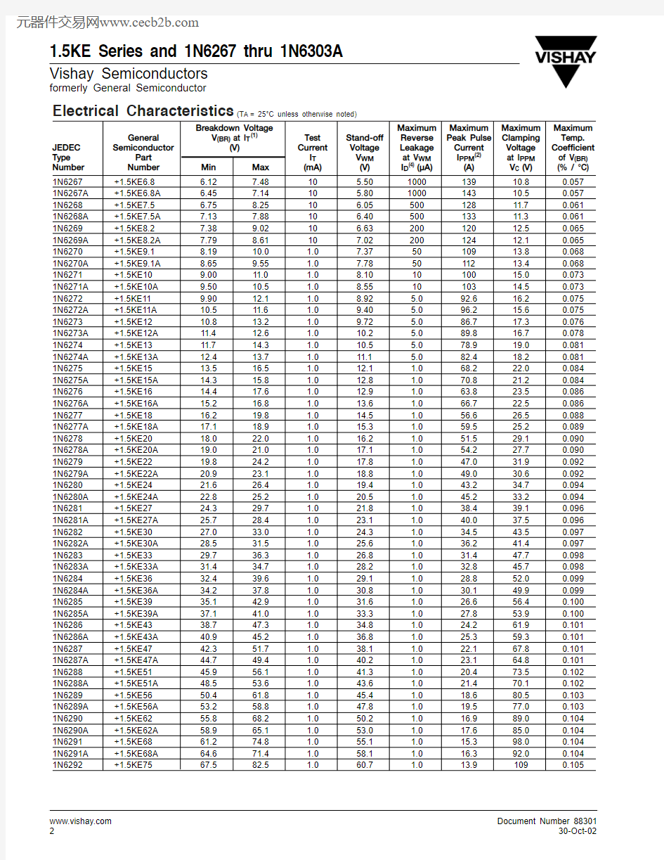
Electrical Characteristics(T A= 25°C unless otherwise noted)
Breakdown Voltage Maximum Maximum Maximum Maximum General V(BR)at I T(1)Test Stand-off Reverse Peak Pulse Clamping Temp. JEDEC Semiconductor(V)Current Voltage Leakage Current Voltage Coefficient Type Part I T V WM at V WM I PPM(2)at I PPM of V(BR) Number Number Min Max(mA)(V)I D(4) (μA)(A)V C (V)(% / °C) 1N6267+1.5KE6.8 6.127.4810 5.50100013910.80.057
1N6267A+1.5KE6.8A 6.457.1410 5.80100014310.50.057
1N6268+1.5KE7.5 6.758.2510 6.0550012811.70.061
1N6268A+1.5KE7.5A7.137.8810 6.4050013311.30.061
1N6269+1.5KE8.27.389.0210 6.6320012012.50.065
1N6269A+1.5KE8.2A7.798.61107.022*******.10.065
1N6270+1.5KE9.18.1910.0 1.07.375010913.80.068
1N6270A+1.5KE9.1A8.659.55 1.07.785011213.40.068
1N6271+1.5KE109.0011.0 1.08.101010015.00.073
1N6271A+1.5KE10A9.5010.5 1.08.551010314.50.073
1N6272+1.5KE119.9012.1 1.08.92 5.092.616.20.075
1N6272A+1.5KE11A10.511.6 1.09.40 5.096.215.60.075
1N6273+1.5KE1210.813.2 1.09.72 5.086.717.30.076
1N6273A+1.5KE12A11.412.6 1.010.2 5.089.816.70.078
1N6274+1.5KE1311.714.3 1.010.5 5.078.919.00.081
1N6274A+1.5KE13A12.413.7 1.011.1 5.082.418.20.081
1N6275+1.5KE1513.516.5 1.012.1 1.068.222.00.084
1N6275A+1.5KE15A14.315.8 1.012.8 1.070.821.20.084
1N6276+1.5KE1614.417.6 1.012.9 1.063.823.50.086
1N6276A+1.5KE16A15.216.8 1.013.6 1.066.722.50.086
1N6277+1.5KE1816.219.8 1.014.5 1.056.626.50.088
1N6277A+1.5KE18A17.118.9 1.015.3 1.059.525.20.089
1N6278+1.5KE2018.022.0 1.016.2 1.051.529.10.090
1N6278A+1.5KE20A19.021.0 1.017.1 1.054.227.70.090
1N6279+1.5KE2219.824.2 1.017.8 1.047.031.90.092
1N6279A+1.5KE22A20.923.1 1.018.8 1.049.030.60.092
1N6280+1.5KE2421.626.4 1.019.4 1.043.234.70.094
1N6280A+1.5KE24A22.825.2 1.020.5 1.045.233.20.094
1N6281+1.5KE2724.329.7 1.021.8 1.038.439.10.096
1N6281A+1.5KE27A25.728.4 1.023.1 1.040.037.50.096
1N6282+1.5KE3027.033.0 1.024.3 1.034.543.50.097
1N6282A+1.5KE30A28.531.5 1.025.6 1.036.241.40.097
1N6283+1.5KE3329.736.3 1.026.8 1.031.447.70.098
1N6283A+1.5KE33A31.434.7 1.028.2 1.032.845.70.098
1N6284+1.5KE3632.439.6 1.029.1 1.028.852.00.099
1N6284A+1.5KE36A34.237.8 1.030.8 1.030.149.90.099
1N6285+1.5KE3935.142.9 1.031.6 1.026.656.40.100
1N6285A+1.5KE39A37.141.0 1.033.3 1.027.853.90.100
1N6286+1.5KE4338.747.3 1.034.8 1.024.261.90.101
1N6286A+1.5KE43A40.945.2 1.036.8 1.025.359.30.101
1N6287+1.5KE4742.351.7 1.038.1 1.022.167.80.101
1N6287A+1.5KE47A44.749.4 1.040.2 1.023.164.80.101
1N6288+1.5KE5145.956.1 1.041.3 1.020.473.50.102
1N6288A+1.5KE51A48.553.6 1.043.6 1.021.470.10.102
1N6289+1.5KE5650.461.8 1.045.4 1.018.680.50.103
1N6289A+1.5KE56A53.258.8 1.047.8 1.019.577.00.103
1N6290+1.5KE6255.868.2 1.050.2 1.016.989.00.104
1N6290A+1.5KE62A58.965.1 1.053.0 1.017.685.00.104
1N6291+1.5KE6861.274.8 1.055.1 1.015.398.00.104
1N6291A+1.5KE68A64.671.4 1.058.1 1.016.392.00.104
1N6292+1.5KE7567.582.5 1.060.7 1.013.91090.105
Electrical Characteristics (Cont’d)(T A= 25°C unless otherwise noted)
Breakdown Voltage Maximum Maximum Maximum Maximum General V(BR)at I T(1)Test Stand-off Reverse Peak Pulse Clamping Temp. JEDEC Semiconductor(V)Current Voltage Leakage Current Voltage Coefficient Type Part I T V WM at V WM I PPM(2)at I PPM of V(BR) Number Number Min Max(mA)(V)I D(4) (μA)(A)V C (V)(% / °C) 1N6292A+1.5KE75A71.378.8 1.064.1 1.014.61040.105
1N6293+1.5KE8273.890.2 1.066.4 1.012.71180.105
1N6293A+1.5KE82A77.986.1 1.070.1 1.013.31130.105
1N6294+1.5KE9181.9100.0 1.073.7 1.011.51310.106
1N6294A+1.5KE91A86.595.5 1.077.8 1.012.01250.106
1N6295+1.5KE10090.0110 1.081.0 1.010.41440.106
1N6295A+1.5KE100A95.0105 1.085.5 1.010.91370.106
1N6296+1.5KE11099.0121 1.089.2 1.09.51580.107
1N6296A+1.5KE 110A105116 1.094.0 1.09.91520.107
1N6297+1.5KE120108132 1.097.2 1.08.71730.107
1N6297A+1.5KE120A114126 1.0102 1.09.11650.107
1N6298+1.5KE130117143 1.0105 1.08.01870.107
1N6298A+1.5KE130A124137 1.0111 1.08.41790.107
1N6299+1.5KE150136165 1.0121 1.07.02150.108
1N6299A+1.5KE150A143158 1.0128 1.07.22070.106
1N6300+1.5KE160144176 1.0130 1.0 6.52300.106
1N6300A+1.5KE160A152168 1.0136 1.0 6.82190.108
1N6301+1.5KE170153187 1.0138 1.0 6.12440.108
1N6301A+1.5KE170A162179 1.0145 1.0 6.42340.108
1N6302 1.5KE180162198 1.0146 1.0 5.82580.108
1N6302A 1.5KE180A171189 1.0154 1.0 6.12460.108
1N6303 1.5KE200180220 1.0162 1.0 5.22870.108
1N6303A 1.5KE200A*190210 1.0171 1.0 5.52740.108
1.5KE220198242 1.0175 1.0 4.43440.108
1.5KE220A*209231 1.0185 1.0 4.63280.108
1.5KE250225275 1.0202 1.0 4.23600.110
1.5KE250A237263 1.0214 1.0 4.43440.110
1.5KE300270330 1.0243 1.0 3.54300.110
1.5KE300A285315 1.0256 1.0 3.64140.110
1.5KE350315385 1.0284 1.0 3.05040.110
1.5KE350A333368 1.0300 1.0 3.14820.110
1.5KE400360440 1.0324 1.0
2.65740.110
1.5KE400A380420 1.0342 1.0
2.75480.110
1.5KE440396484 1.0356 1.0
2.46310.110
1.5KE440A418462 1.0376 1.0
2.56020.110
1.5KE480432528 1.0389 1.0
2.196860.110
1.5KE480A456504 1.0408 1.0
2.286580.110
1.5KE510459561 1.0413 1.0
2.067290.110
1.5KE510A485535 1.0434 1.0
2.156980.110
1.5KE540486594 1.0437 1.0 1.947720.110
1.5KE540A513567 1.0459 1.0
2.037400.110 Notes:(1) Pulse test: t p ≤50ms
(2) Surge current waveform per Fig. 3 and derate per Fig. 2
(3) All terms and symbols are consistent with ANSI/IEEE CA62.35
(4) For bidirectional types with V R10 volts and less the I D limit is doubled
* Bidirectional versions are UL approved under component across the line protection, ULV1414 file number E108274 (1.5KE200CA, 1.5KE220CA) + Underwriters Laboratory Recognition for the classification of protectors (QVGQ2) under the UL standard for safety 497B and file number E136766 for both uni-directional and bi-directional devices
Application
? This series of Silicon Transient Suppressors is used in applications where large voltage transients can permanently damage voltage-sensitive components.? The TVS diode can be used in applications where induced lightning on rural or remote transmission lines presents a hazard to electronic circuitry
(ref: R.E.A. specification P.E. 60).
? This Transient Voltage Suppressor diode has a pulse power rating of 1500 watts for one millisecond. The response time of TVS diode clamping action is effectively instantaneous (1 x 10⁻⁹seconds bidirectional); therefore, they can protect integrated circuits, MOS devices, hybrids, and other voltage sensitive semiconductors and components. TVS diodes can also be used in series or parallel to increase the peak power ratings.
50
100
150
200
025
50
75
100
25
75
125
175
5
10
100
500
10
100
1,000
10,000
110100
10
100
200
25
50
75
100
125
150
175
200
01.02.03.05.04.06.08.07.0P e a k P u l s e P o w e r (P P P ) o r C u r r e n t (I P P )D e r a t i n g i n P e r c e n t a g e , %
T A — Ambient Temperature (°C)
Fig. 2 – Pulse Derating Curve
Fig. 4 - Typical Junction Capacitance
Fig. 6 - Maximum Non-repetitive Peak Forward
Surge Current Unidirectional Only
C J , C a p a c i t a n c e , p F
V (BR), Breakdown Voltage (V)
P
M (A V ), S t e a d y S t a t e P o w e r D i s s i p a t i o n (W )
Fig. 5 – Steady State Power
Derating Curve
T L — Lead Temperature (°C)
P e a k F o r w a r d S u r g e C u r r e n t
(A )
Number of Cycles at 60 H Z
I P P M — P e a k P
u l s e C u r r e n t , % I R S M
Fig. 3 – Pulse Waveform
2.0
t — Time (ms)
P P P M — P e a k P u l s e P o w e r (k W )
Fig. 1 – Peak Pulse Power Rating Curve
0.1
1
10
100
0.1μs 1.0μs 10μs t d — Pulse Width (sec.)100μs 1.0ms 10ms
Ratings and
Characteristic Curves (T A = 25°C unless otherwise noted)
Ratings and
Characteristic Curves (T A = 25°C unless otherwise noted)
0.1
0.21.0
2.010
201000.5
1
2.0
102050
0.1
0.21.0
2.010
201000.5
1
2.0
102050
Fig. 7 – Incremental Clamping Voltage
Curve (Unidirectional)
?V C , I n c r e m e n t a l C l a m p i n g V o l t a g e
?V C , I n c r e m e n t a l C l a m p i n g V o l t a g e
I PP , Peak Pulse Current (A)
Fig. 8 – Incremental Clamping Voltage
Curve (Unidirectional)
I PP , Peak Pulse Current (A)
0.4
0.8
1.2
1.6
2.0
0.1
110
100
Fig. 11 – Instantaneous Forward Voltage
Characteristics Curve
Fig. 13 – Typical Reverse Leakage
Characteristics
I n s t a n t a n e o u s F o r w a r d C u r r e n t (A )
Instantaneous Forward Voltage (V)
T r a n s i e n t T h e r m a l I m p e d a n c e (°C /W )
10
100
1
0.10.001
t p – Pulse Duration (sec)
0.01
0.1
1
10
100
1000
Fig. 12 – Typical Transient
Thermal Impedance
600
100
200
300
400
500
0.01
0.1
1.0
100
10
1000
R e v e r s e L e a k a g e C u r r e n t (μA )
Breakdown Voltage (V)
Ratings and
Characteristic Curves (T A = 25°C unless otherwise noted)