https://www.doczj.com/doc/6612370807.html,
FEATURES
DESCRIPTION/ORDERING INFORMATION
1 2 3 48 7 6 5
GND TRIG
OUT RESET V
CC
DISCH
THRES
CONT
3212019
910111213
4
5
6
7
8
18
17
16
15
14
NC
DISCH
NC
THRES
NC
NC
TRIG
NC
OUT
NC
N
C
G
N
D
N
C
C
O
N
T
N
C
V
C
C
N
C
N
C
R
E
S
E
T
N
C
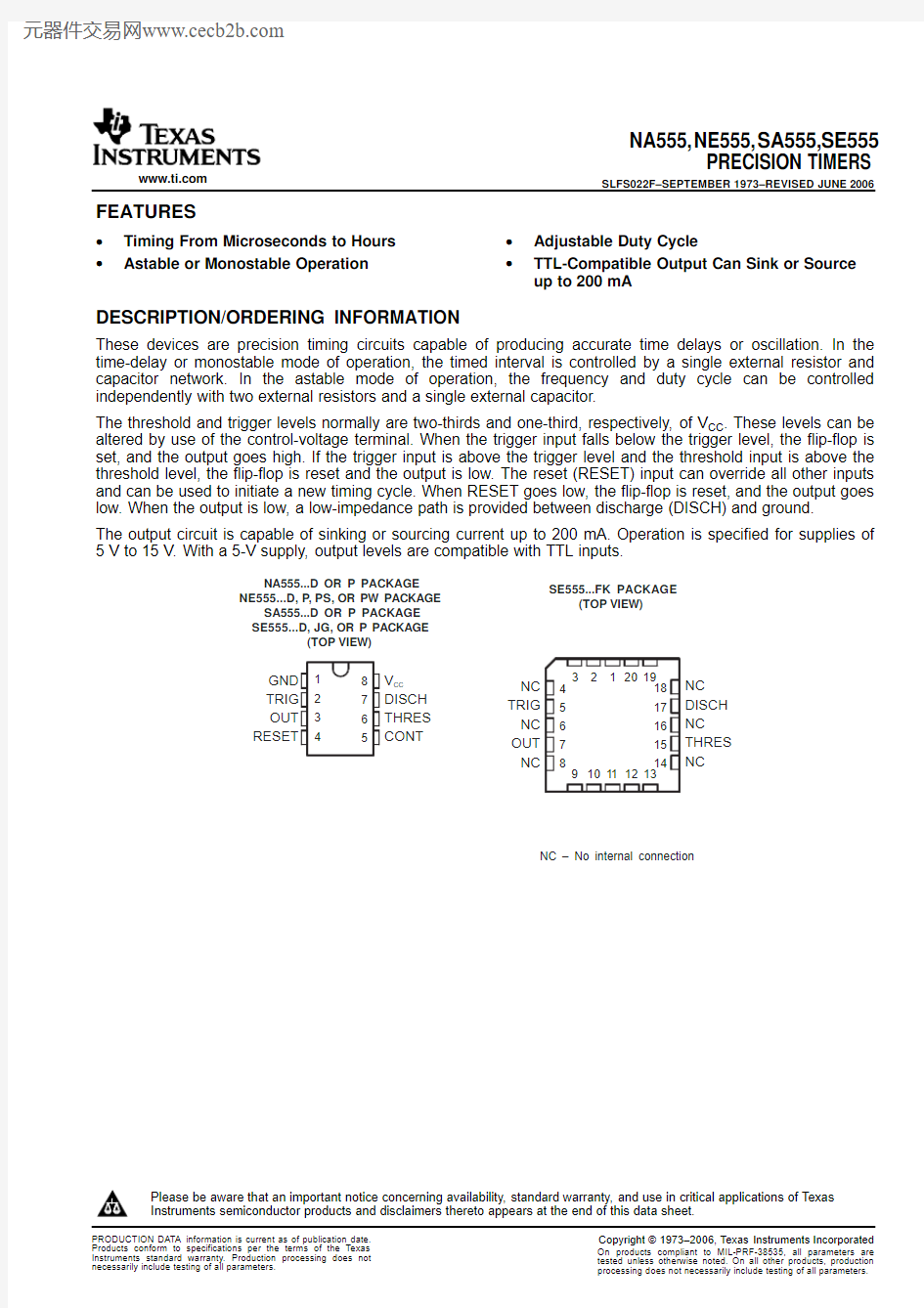
NC – No internal connection
NA555...D OR P PACKAGE
NE555...D,P,PS,OR PW PACKAGE SA555...D OR P PACKAGE
SE555...D,JG,OR P PACKAGE
(TOP VIEW)SE555...FK PACKAGE
(TOP VIEW)
NA555,NE555,SA555,SE555
PRECISION TIMERS SLFS022F–SEPTEMBER1973–REVISED JUNE2006
?Timing From Microseconds to Hours?Adjustable Duty Cycle
?Astable or Monostable Operation?TTL-Compatible Output Can Sink or Source
up to200mA
These devices are precision timing circuits capable of producing accurate time delays or oscillation.In the time-delay or monostable mode of operation,the timed interval is controlled by a single external resistor and capacitor network.In the astable mode of operation,the frequency and duty cycle can be controlled independently with two external resistors and a single external capacitor.
The threshold and trigger levels normally are two-thirds and one-third,respectively,of V CC.These levels can be altered by use of the control-voltage terminal.When the trigger input falls below the trigger level,the flip-flop is set,and the output goes high.If the trigger input is above the trigger level and the threshold input is above the threshold level,the flip-flop is reset and the output is low.The reset(RESET)input can override all other inputs and can be used to initiate a new timing cycle.When RESET goes low,the flip-flop is reset,and the output goes low.When the output is low,a low-impedance path is provided between discharge(DISCH)and ground.
The output circuit is capable of sinking or sourcing current up to200mA.Operation is specified for supplies of 5V to15V.With a5-V supply,output levels are compatible with TTL inputs.
Please be aware that an important notice concerning availability,standard warranty,and use in critical applications of Texas
Instruments semiconductor products and disclaimers thereto appears at the end of this data sheet.
https://www.doczj.com/doc/6612370807.html,
NA555,NE555,SA555,SE555PRECISION TIMERS
SLFS022F–SEPTEMBER 1973–REVISED JUNE 2006
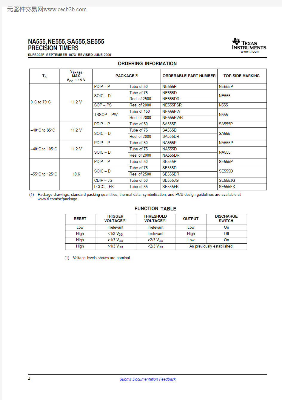
ORDERING INFORMATION
V THRES T A
MAX PACKAGE (1)
ORDERABLE PART NUMBER TOP-SIDE MARKING V CC =15V
PDIP –P Tube of 50NE555P NE555P Tube of 75NE555D SOIC –D
NE555Reel of 2500NE555DR 0°C to 70°C
11.2V
SOP –PS Reel of 2000NE555PSR N555Tube of 150NE555PW TSSOP –PW N555Reel of 2000NE555PWR PDIP –P
Tube of 50SA555P SA555P –40°C to 85°C
11.2V
Tube of 75SA555D SOIC –D SA555Reel of 2000SA555DR PDIP –P
Tube of 50NA555P NA555P –40°C to 105°C
11.2V
Tube of 75NA555D SOIC –D NA555Reel of 2000NA555DR PDIP –P
Tube of 50SE555P SE555P Tube of 75SE555D SOIC –D SE555D –55°C to 125°C
10.6
Reel of 2500SE555DR CDIP –JG Tube of 50SE555JG SE555JG LCCC –FK
Tube of 55
SE555FK
SE555FK
(1)
Package drawings,standard packing quantities,thermal data,symbolization,and PCB design guidelines are available at https://www.doczj.com/doc/6612370807.html,/sc/package.
FUNCTION TABLE
TRIGGER THRESHOLD DISCHARGE RESET OUTPUT VOLTAGE (1)VOLTAGE (1)SWITCH
Low Irrelevant Irrelevant Low On High <1/3V DD Irrelevant High Off High >1/3V DD >2/3V DD Low
On
High
>1/3V DD
<2/3V DD
As previously established
(1)
Voltage levels shown are nominal.
https://www.doczj.com/doc/6612370807.html,
TRIG
THRES
OUT
DISCH
Pin numbers shown are for the D, JG, P , PS, and PW packages.NOTE A:RESET can override TRIG, which can override THRES.
NA555,NE555,SA555,SE555
PRECISION TIMERS
SLFS022F–SEPTEMBER 1973–REVISED JUNE 2006
FUNCTIONAL BLOCK DIAGRAM
https://www.doczj.com/doc/6612370807.html,
Absolute Maximum Ratings (1)
Recommended Operating Conditions
NA555,NE555,SA555,SE555PRECISION TIMERS
SLFS022F–SEPTEMBER 1973–REVISED JUNE 2006
over operating free-air temperature range (unless otherwise noted)
MIN
MAX UNIT V CC Supply voltage (2)18V V I Input voltage CONT,RESET,THRES,TRIG
V CC V I O
Output current
±225mA
D package
97P package 85θJA
Package thermal impedance (3)(4)
°C/W PS package 95PW package
149FK package 5.61θJC Package thermal impedance (5)(6)°C/W JG package
14.5T J
Operating virtual junction temperature 150°C Case temperature for 60s
FK package 260°C Lead temperature 1,6mm (1/16in)from case for 60s
JG package
300°C T stg Storage temperature range
–65
150
°C (1)Stresses beyond those listed under "absolute maximum ratings"may cause permanent damage to the device.These are stress ratings only,and functional operation of the device at these or any other conditions beyond those indicated under "recommended operating conditions"is not implied.Exposure to absolute-maximum-rated conditions for extended periods may affect device reliability.(2)All voltage values are with respect to GND.
(3)Maximum power dissipation is a function of T J (max),θJA ,and T A .The maximum allowable power dissipation at any allowable ambient temperature is P D =(T J (max)-T A )/θJA.Operating at the absolute maximum T J of 150°C can affect reliability.(4)The package thermal impedance is calculated in accordance with JESD 51-7.
(5)Maximum power dissipation is a function of T J (max),θJC ,and T C .The maximum allowable power dissipation at any allowable case temperature is P D =(T J (max)-T C )/θJC .Operating at the absolute maximum T J of 150°C can affect reliability.(6)
The package thermal impedance is calculated in accordance with MIL-STD-883.
over operating free-air temperature range (unless otherwise noted)
MIN
MAX UNIT NA555,NE555,SA555 4.516V CC Supply voltage V SE555
4.5
18V I Input voltage CONT,RESET,THRES,and TRIG
V CC V I O
Output current
±200mA
NA555
–40105NE555070T A
Operating free-air temperature
°C SA555–4085SE555
–55
125
https://www.doczj.com/doc/6612370807.html,
Electrical Characteristics
NA555,NE555,SA555,SE555
PRECISION TIMERS SLFS022F–SEPTEMBER1973–REVISED JUNE2006
V CC =5V to15V,T
A
=25°C(unless otherwise noted)
NA555
SE555NE555
PARAMETER TEST CONDITIONS UNIT
SA555
MIN TYP MAX MIN TYP MAX V CC=15V9.41010.68.81011.2
THRES voltage level V V CC=5V 2.7 3.34 2.4 3.3 4.2
THRES current(1)3025030250nA
4.85
5.2 4.55 5.6
V CC=15V
T A=–55°C to125°C36
TRIG voltage level V
1.45 1.67 1.9 1.1 1.67
2.2
V CC=5V
T A=–55°C to125°C 1.9
TRIG current TRIG at0V0.50.90.52μA
0.30.710.30.71 RESET voltage level V T A=–55°C to125°C 1.1
RESET at V CC0.10.40.10.4 RESET current mA RESET at0V–0.4–1–0.4–1.5
DISCH switch off-state
2010020100nA current
9.61010.491011
V CC=15V
T A=–55°C to125°C9.610.4
CONT voltage
V (open circuit) 2.9 3.3 3.8 2.6 3.34
V CC=5V
T A=–55°C to125°C 2.9 3.8
0.10.150.10.25
V CC=15V,I OL=10mA
T A=–55°C to125°C0.2
0.40.50.40.75
V CC=15V,I OL=50mA
T A=–55°C to125°C1
2 2.22 2.5
V CC=15V,I OL=100mA
Low-level output voltage T A=–55°C to125°C 2.7V
V CC=15V,I OL=200mA 2.5 2.5
V CC=5V,I OL=3.5mA T A=–55°C to125°C0.35
0.10.20.10.35
V CC=5V,I OL=5mA
T A=–55°C to125°C0.8
V CC=5V,I OL=8mA0.150.250.150.4
1313.312.7513.3
V CC=15V,I OL=–100mA
T A=–55°C to125°C12
High-level output voltage V CC=15V,I OH=–200mA12.512.5V
3 3.3 2.75 3.3
V CC=15V,I OL=–100mA
T A=–55°C to125°C2
V CC=15V10121015
Output low,No load
V CC=5V3536 Supply current mA
V CC=15V910913
Output high,No load
V CC=5V2425
(1)This parameter influences the maximum value of the timing resistors R A and R B in the circuit of Figure12.For example,
when V CC=5V,the maximum value is R=R A+R B≈3.4M?,and for V CC=15V,the maximum value is10M?.
https://www.doczj.com/doc/6612370807.html,
Operating Characteristics
NA555,NE555,SA555,SE555PRECISION TIMERS
SLFS022F–SEPTEMBER 1973–REVISED JUNE 2006
V CC =5V to 15V,T A =25°C (unless otherwise noted)
NA555SE555NE555TEST
PARAMETER
UNIT
SA555CONDITIONS (1)
MIN
TYP MAX MIN
TYP MAX
Each timer,monostable (3)T A =25°C
0.5 1.5(4)
13
Initial error of timing %interval (2)
Each timer,astable (5) 1.5 2.25Each timer,monostable (3)T A =MIN to MAX 30100(4)50Temperature coefficient of ppm/timing interval
°C Each timer,
astable (5)
90150Each timer,monostable (3)
T A =25°C 0.050.2(4)0.10.5Supply-voltage sensitivity of %/V timing interval Each timer,astable (5)
0.150.3C L =15pF,Output-pulse rise time 100200(4)100300ns T A =25°C C L =15pF,Output-pulse fall time 100
200(4)100
300ns T A =25°C (1)For conditions shown as MIN or MAX,use the appropriate value specified under recommended operating conditions.
(2)Timing interval error is defined as the difference between the measured value and the average value of a random sample from each process run.
(3)Values specified are for a device in a monostable circuit similar to Figure 9,with the following component values:R A =2k ?to 100k ?,C =0.1μF.
(4)On products compliant to MIL-PRF-38535,this parameter is not production tested.
(5)
Values specified are for a device in an astable circuit similar to Figure 12,with the following component values:R A =1k ?to 100k ?,C =0.1μF.
https://www.doczj.com/doc/6612370807.html,
TYPICAL CHARACTERISTICS
I OL ? Low-Level Output Current ? mA
LOW-LEVEL OUTPUT VOLTAGE
vs
LOW-LEVEL OUTPUT CURRENT
? L o w -L e v e l O u t p u t V o l t a g e ? V
V O L
LOW-LEVEL OUTPUT VOLTAGE
vs
LOW-LEVEL OUTPUT CURRENT
? L o w -L e v e l O u t p u t V o l t a g e ? V
V O L I OL ? Low-Level Output Current ? mA
0.020.22
LOW-LEVEL OUTPUT VOLTAGE
vs
LOW-LEVEL OUTPUT CURRENT
? L o w -L e v e l O u t p u t V o l t a g e
? V
V O L I OL ? Low-Level Output Current ? mA 10.60.20
1.41.8
2.0
0.41.60.81.2? I OH ? High-Level Output Current ? mA
V C C V O H ? V o l t a g e D r o p ? V
)(DROP BETWEEN SUPPLY VOLTAGE AND OUTPUT
vs
HIGH-LEVEL OUTPUT CURRENT
NA555,NE555,SA555,SE555
PRECISION TIMERS
SLFS022F–SEPTEMBER 1973–REVISED JUNE 2006
Data for temperatures below 0°C and above 70°C are applicable for SE555circuits only.Figure 1.Figure 2.
Figure 3.Figure 4.
https://www.doczj.com/doc/6612370807.html,
5
6
7
8
9
10
11
? S u p p l y C u r r e n t ? m A
SUPPLY CURRENT
vs
SUPPLY VOLTAGE
12
13
14
15
C C I V CC ? Supply Voltage ? V
1
0.995
0.990
0.985
5
10
1.005
1.010
NORMALIZED OUTPUT PULSE DURATION
(MONOSTABLE OPERATION)
vs
SUPPLY VOLTAGE
1.015
15
20
C C
V P u l s e D u r a t i o n
R e l a t i v e t o V a l u e a t = 10 V V CC ? Supply Voltage ? V
?75
?25
25
NORMALIZED OUTPUT PULSE DURATION
(MONOSTABLE OPERATION)
vs
FREE-AIR TEMPERATURE
75
125
T A ? Free-Air Temperature ? °C
?50
50
100P u l s e D u r a t i o n R e l a t i v e t o V a l u e a t T A = 255C
? P r o p a g a t i o n D e l a y T i m e ? n s
PROPAGATION DELAY TIME
vs
LOWEST VOLTAGE LEVEL OF TRIGGER PULSE
Lowest Voltage Level of Trigger Pulse
t P D 0
0.1 x V CC
0.2 x V CC
0.3 x V CC
0.4 x V CC
NA555,NE555,SA555,SE555PRECISION TIMERS
SLFS022F–SEPTEMBER 1973–REVISED JUNE 2006
TYPICAL CHARACTERISTICS (continued)
Data for temperatures below 0°C and above 70°C are applicable for SE555circuits only.
Figure 5.Figure 6.
Figure 7.Figure 8.
https://www.doczj.com/doc/6612370807.html,
APPLICATION INFORMATION
Monostable Operation
V CC
(5 V to 15 V)
Output
Input
Pin numbers shown are for the D, JG, P , PS, and PW packages.
NA555,NE555,SA555,SE555
PRECISION TIMERS
SLFS022F–SEPTEMBER 1973–REVISED JUNE 2006
For monostable operation,any of these timers can be connected as shown in Figure 9.If the output is low,application of a negative-going pulse to the trigger (TRIG)sets the flip-flop (Q goes low),drives the output high,and turns off Q1.Capacitor C then is charged through R A until the voltage across the capacitor reaches the threshold voltage of the threshold (THRES)input.If TRIG has returned to a high level,the output of the threshold comparator resets the flip-flop (Q goes high),drives the output low,and discharges C through Q1.
Figure 9.Circuit for Monostable Operation
Monostable operation is initiated when TRIG voltage falls below the trigger threshold.Once initiated,the sequence ends only if TRIG is high at the end of the timing interval.Because of the threshold level and saturation voltage of Q1,the output pulse duration is approximately t w =1.1R A C.Figure 11is a plot of the time constant for various values of R A and C.The threshold levels and charge rates both are directly proportional to the supply voltage,V CC .The timing interval is,therefore,independent of the supply voltage,so long as the supply voltage is constant during the time interval.
Applying a negative-going trigger pulse simultaneously to RESET and TRIG during the timing interval discharges C and reinitiates the cycle,commencing on the positive edge of the reset pulse.The output is held low as long as the reset pulse is low.To prevent false triggering,when RESET is not used,it should be connected to V CC .
https://www.doczj.com/doc/6612370807.html,
? O u t p u t P u l s e D u r a t i o n ? s
C ? Capacitance ? μF
10
1
10?1
10?2
10?3
10?4
10?5
t w V o l t a g e ? 2 V /d i v
Time ? 0.1 ms/div
Astable Operation
V o l t a g e ? 1 V /d i v
Time ? 0.5 ms/div
t
t
R R Output
L V CC
NOTE A:Decoupling CONT voltage to ground with a capacitor can
improve operation. This should be evaluated for individual applications.
Pin numbers shown are for the D, JG, P , PS, and PW packages.
NA555,NE555,SA555,SE555PRECISION TIMERS
SLFS022F–SEPTEMBER 1973–REVISED JUNE 2006
APPLICATION INFORMATION (continued)
Figure 10.Typical Monostable Waveforms Figure 11.Output Pulse Duration vs Capacitance
As shown in Figure 12,adding a second resistor,R B ,to the circuit of Figure 9and connecting the trigger input to the threshold input causes the timer to self-trigger and run as a multivibrator.The capacitor C charges through R A and R B and then discharges through R B only.Therefore,the duty cycle is controlled by the values of R A and R B .
This astable connection results in capacitor C charging and discharging between the threshold-voltage level (≈0.67×V CC )and the trigger-voltage level (≈0.33×V CC ).As in the monostable circuit,charge and discharge times (and,therefore,the frequency and duty cycle)are independent of the supply voltage.
Figure 12.Circuit for Astable Operation Figure 13.Typical Astable Waveforms
https://www.doczj.com/doc/6612370807.html,
t
H
+0.693(R A )R B)
C
t L +0.693(R B)C Other useful relationships are shown below.
period +t H )t L +0.693(R A )2R B
)C
frequency [
1.44(R A )2R B )C Output driver duty cycle +
t
L t H )t L +R
B R A )2R B Output waveform duty cycle
+t L t H +R B R A )R B
Low-to-high ratio +t H t H )t L +1–R B R A )2R B
f ? F r e e -R u n n i n
g F r e q u e n c y ? H z
C ? Capacitance ? μF
100
10
1
0.1
0.01
0.001
Missing-Pulse
Detector
Time ? 0.1 ms/div
V o l t a g e ? 2 V /d i v
Pin numbers shown are shown for the D, JG, P , PS, and PW packages.
NA555,NE555,SA555,SE555
PRECISION TIMERS
SLFS022F–SEPTEMBER 1973–REVISED JUNE 2006
APPLICATION INFORMATION (continued)
Figure 13shows typical waveforms generated during astable operation.The output high-level duration t H and low-level duration t L can be calculated as follows:
Figure 14.Free-Running Frequency
The circuit shown in Figure 15can be used to detect a missing pulse or abnormally long spacing between consecutive pulses in a train of pulses.The timing interval of the monostable circuit is retriggered continuously by the input pulse train as long as the pulse spacing is less than the timing interval.A longer pulse spacing,missing pulse,or terminated pulse train permits the timing interval to be completed,thereby generating an output pulse as shown in Figure 16.
Figure 15.Circuit for Missing-Pulse Detector
Figure https://www.doczj.com/doc/6612370807.html,pleted Timing Waveforms for
Missing-Pulse Detector
https://www.doczj.com/doc/6612370807.html,
Frequency Divider
V o l t a g e ? 2 V /d i v
Time ? 0.1 ms/div
NA555,NE555,SA555,SE555PRECISION TIMERS
SLFS022F–SEPTEMBER 1973–REVISED JUNE 2006
APPLICATION INFORMATION (continued)
By adjusting the length of the timing cycle,the basic circuit of Figure 9can be made to operate as a frequency divider.Figure 17shows a divide-by-three circuit that makes use of the fact that retriggering cannot occur during the timing cycle.
Figure 17.Divide-by-Three Circuit Waveforms
https://www.doczj.com/doc/6612370807.html,
Pulse-Width Modulation
C
A
V (5 V to 15 V)
Output
Modulation
Input
(see Note A)
Clock Input
NOTE A:The modulating signal can be direct or capacitively coupled
to CONT . For direct coupling, the effects of modulation source voltage and impedance on the bias of the timer should be considered.
Pin numbers shown are for the D, JG, P , PS, and PW packages.
V o l t a g e ? 2 V /d i v
Time ? 0.5 ms/div
NA555,NE555,SA555,SE555
PRECISION TIMERS
SLFS022F–SEPTEMBER 1973–REVISED JUNE 2006
APPLICATION INFORMATION (continued)
The operation of the timer can be modified by modulating the internal threshold and trigger voltages,which is accomplished by applying an external voltage (or current)to CONT.Figure 18shows a circuit for pulse-width modulation.A continuous input pulse train triggers the monostable circuit,and a control signal modulates the threshold voltage.Figure 19shows the resulting output pulse-width modulation.While a sine-wave modulation signal is shown,any wave shape could be used.
Figure 18.Circuit for Pulse-Width Modulation Figure 19.Pulse-Width-Modulation Waveforms
https://www.doczj.com/doc/6612370807.html,
Pulse-Position Modulation
V o l t a g e ? 2 V /d i v
Time ? 0.1 ms/div
NOTE A:The modulating signal can be direct or capacitively coupled
to CONT . For direct coupling, the effects of modulation source voltage and impedance on the bias of the timer should be considered.
Pin numbers shown are for the D, JG, P , PS, and PW packages.
Output
NA555,NE555,SA555,SE555PRECISION TIMERS
SLFS022F–SEPTEMBER 1973–REVISED JUNE 2006
APPLICATION INFORMATION (continued)
As shown in Figure 20,any of these timers can be used as a pulse-position modulator.This application modulates the threshold voltage and,thereby,the time delay,of a free-running oscillator.Figure 21shows a triangular-wave modulation signal for such a circuit;however,any wave shape could be used.
Figure 20.Circuit for Pulse-Position Modulation Figure 21.Pulse-Position-Modulation Waveforms
https://www.doczj.com/doc/6612370807.html,
Sequential Timer
C B = 4.7 μF R B = 100 k ?
Pin numbers shown are for the D, JG, P , PS, and PW packages.NOTE A:S closes momentarily at t = 0.
V o l t a g e ? 5 V /d i v
t ? Time ? 1 s/div
NA555,NE555,SA555,SE555
PRECISION TIMERS
SLFS022F–SEPTEMBER 1973–REVISED JUNE 2006
APPLICATION INFORMATION (continued)
Many applications,such as computers,require signals for initializing conditions during start-up.Other applications,such as test equipment,require activation of test signals in sequence.These timing circuits can be connected to provide such sequential control.The timers can be used in various combinations of astable or monostable circuit connections,with or without modulation,for extremely flexible waveform control.Figure 22shows a sequencer circuit with possible applications in many systems,and Figure 23shows the output waveforms.
Figure 22.Sequential Timer Circuit
Figure 23.Sequential Timer Waveforms
PACKAGING INFORMATION
Orderable
Device Status (1)Package Type Package Drawing Pins Package Qty Eco Plan (2)
Lead/Ball Finish MSL Peak Temp (3)JM38510/10901BPA
ACTIVE CDIP JG 81TBD A42SNPB N /A for Pkg Type NA555D ACTIVE SOIC D 875Green (RoHS &no Sb/Br)CU NIPDAU Level-1-260C-UNLIM NA555DG4ACTIVE SOIC D 875
Green (RoHS &no Sb/Br)
CU NIPDAU Level-1-260C-UNLIM NA555DR ACTIVE SOIC D 82500Green (RoHS &
no Sb/Br)CU NIPDAU Level-1-260C-UNLIM NA555DRG4ACTIVE SOIC D 82500Green (RoHS &
no Sb/Br)CU NIPDAU Level-1-260C-UNLIM NA555P ACTIVE PDIP P 850Pb-Free (RoHS)CU NIPDAU N /A for Pkg Type NA555PE4ACTIVE PDIP P 850Pb-Free (RoHS)CU NIPDAU N /A for Pkg Type NE555D ACTIVE SOIC D 875Green (RoHS &no Sb/Br)CU NIPDAU Level-1-260C-UNLIM NE555DE4ACTIVE SOIC D 875Green (RoHS &no Sb/Br)CU NIPDAU Level-1-260C-UNLIM NE555DG4ACTIVE SOIC D 875
Green (RoHS &no Sb/Br)
CU NIPDAU Level-1-260C-UNLIM NE555DR ACTIVE SOIC D 82500Green (RoHS &
no Sb/Br)CU NIPDAU Level-1-260C-UNLIM NE555DRE4ACTIVE SOIC D 82500Green (RoHS &
no Sb/Br)CU NIPDAU Level-1-260C-UNLIM NE555DRG4ACTIVE SOIC D 82500Green (RoHS &
no Sb/Br)CU NIPDAU Level-1-260C-UNLIM NE555P ACTIVE PDIP P 850Pb-Free (RoHS)CU NIPDAU N /A for Pkg Type NE555PE4ACTIVE PDIP P 850
Pb-Free (RoHS)CU NIPDAU N /A for Pkg Type NE555PSLE OBSOLETE SO PS 8TBD
Call TI Call TI
NE555PSR ACTIVE SO PS 82000Green (RoHS &
no Sb/Br)CU NIPDAU Level-1-260C-UNLIM NE555PSRE4ACTIVE SO PS 82000Green (RoHS &
no Sb/Br)CU NIPDAU Level-1-260C-UNLIM NE555PW ACTIVE TSSOP PW 8150Green (RoHS &no Sb/Br)CU NIPDAU Level-1-260C-UNLIM NE555PWE4ACTIVE TSSOP PW 8150
Green (RoHS &no Sb/Br)
CU NIPDAU Level-1-260C-UNLIM NE555PWR ACTIVE TSSOP PW 82000Green (RoHS &
no Sb/Br)CU NIPDAU Level-1-260C-UNLIM NE555PWRE4ACTIVE TSSOP
PW
82000Green (RoHS &
no Sb/Br)
CU NIPDAU Level-1-260C-UNLIM NE555Y OBSOLETE 0TBD Call TI Call TI
SA555D ACTIVE SOIC D 875Green (RoHS &no Sb/Br)CU NIPDAU Level-1-260C-UNLIM SA555DE4ACTIVE SOIC D 875Green (RoHS &no Sb/Br)CU NIPDAU Level-1-260C-UNLIM SA555DG4
ACTIVE
SOIC
D
8
75Green (RoHS &no Sb/Br)
CU NIPDAU
Level-1-260C-UNLIM
https://www.doczj.com/doc/6612370807.html,
31-Jul-2006
Orderable Device
Status (1)Package Type Package Drawing
Pins Package Qty Eco Plan (2)
Lead/Ball Finish MSL Peak Temp (3)SA555DR ACTIVE SOIC D 82500Green (RoHS &
no Sb/Br)CU NIPDAU Level-1-260C-UNLIM SA555DRE4ACTIVE SOIC D 82500Green (RoHS &
no Sb/Br)CU NIPDAU Level-1-260C-UNLIM SA555DRG4ACTIVE SOIC D 82500Green (RoHS &
no Sb/Br)CU NIPDAU Level-1-260C-UNLIM SA555P ACTIVE PDIP P 850Pb-Free (RoHS)CU NIPDAU N /A for Pkg Type SA555PE4ACTIVE PDIP P 850Pb-Free (RoHS)CU NIPDAU N /A for Pkg Type SE555D ACTIVE SOIC D 875TBD CU NIPDAU Level-1-220C-UNLIM SE555DR ACTIVE SOIC D 82500TBD CU NIPDAU Level-1-220C-UNLIM SE555FKB ACTIVE LCCC FK 201TBD POST-PLATE N /A for Pkg Type
SE555JG ACTIVE CDIP JG 81TBD A42SNPB N /A for Pkg Type SE555JGB ACTIVE CDIP JG 81
TBD A42SNPB N /A for Pkg Type SE555N OBSOLETE PDIP N 8TBD Call TI Call TI
SE555P
ACTIVE
PDIP
P
8
50
Pb-Free (RoHS)
CU NIPDAU
N /A for Pkg Type
(1)
The marketing status values are defined as follows:ACTIVE:Product device recommended for new designs.
LIFEBUY:TI has announced that the device will be discontinued,and a lifetime-buy period is in effect.
NRND:Not recommended for new designs.Device is in production to support existing customers,but TI does not recommend using this part in a new design.
PREVIEW:Device has been announced but is not in production.Samples may or may not be available.OBSOLETE:TI has discontinued the production of the device.
(2)
Eco Plan -The planned eco-friendly classification:Pb-Free (RoHS),Pb-Free (RoHS Exempt),or Green (RoHS &no Sb/Br)-please check https://www.doczj.com/doc/6612370807.html,/productcontent for the latest availability information and additional product content details.TBD:The Pb-Free/Green conversion plan has not been defined.
Pb-Free (RoHS):TI's terms "Lead-Free"or "Pb-Free"
mean semiconductor products that are compatible with the current RoHS requirements for all 6substances,including the requirement that lead not exceed 0.1%by weight in homogeneous materials.Where designed to be soldered at high temperatures,TI Pb-Free products are suitable for use in specified lead-free processes.
Pb-Free (RoHS Exempt):This component has a RoHS exemption for either 1)lead-based flip-chip solder bumps used between the die and package,or 2)lead-based die adhesive used between the die and leadframe.The component is otherwise considered Pb-Free (RoHS compatible)as defined above.
Green (RoHS &no Sb/Br):TI defines "Green"to mean Pb-Free (RoHS compatible),and free of Bromine (Br)and Antimony (Sb)based flame retardants (Br or Sb do not exceed 0.1%by weight in homogeneous material)
(3)
MSL,Peak Temp.--The Moisture Sensitivity Level rating according to the JEDEC industry standard classifications,and peak solder temperature.
Important Information and Disclaimer:The information provided on this page represents TI's knowledge and belief as of the date that it is provided.TI bases its knowledge and belief on information provided by third parties,and makes no representation or warranty as to the accuracy of such information.Efforts are underway to better integrate information from third parties.TI has taken and continues to take reasonable steps to provide representative and accurate information but may not have conducted destructive testing or chemical analysis on incoming materials and chemicals.TI and TI suppliers consider certain information to be proprietary,and thus CAS numbers and other limited information may not be available for release.
In no event shall TI's liability arising out of such information exceed the total purchase price of the TI part(s)at issue in this document sold by TI to Customer on an annual basis.
https://www.doczj.com/doc/6612370807.html,
31-Jul-2006