Advance Product Information
This document contains information for a new product.
Cirrus Logic reserves the right to modify this product without notice.
Copyright ? Cirrus Logic, Inc. 2006
(All Rights Reserved)
CS5467
Four-channel Power/Energy IC
Features
?Energy Data Linearity: ±0.1% of Reading over 1000:1 Dynamic Range ?On-chip Functions:
-Instantaneous Voltage, Current, and Power
-I RMS and V RMS , Active, Reactive, and Apparent Power
-Current Fault and Voltage Sag Detect
-System Calibrations / Phase Compensation -Temperature Sensor
-Energy-to-pulse Conversion
-Positive-only Accumulation Mode
?Meets Accuracy Spec for IEC, ANSI, & JIS ?Low Power Consumption
?GND-referenced Signals with Single Supply ?On-chip, 2.5V Reference ?Power Supply Monitor
?Simple Three-wire Digital Serial Interface ?“Auto-boot” Mode from Serial E 2PROM.?Power Supply Configurations
VA+ = +5V; AGND = 0V; VD+ = +3.3V to +5V
Description
The CS5467 is an integrated power measure-ment device which combines four ?Σanalog-to-digital converters, power calculation engine, energy-to-frequency converter, and a serial interface on a single chip. It is designed to accurately measure instantaneous current and voltage and calculate V RMS , I RMS , instantaneous power, active power, apparent power, and reac-tive power for high-performance power measurement applications.
The CS5467 is optimized to interface to shunt re-sistors or current transformers for current measurement, and to resistive dividers or poten-tial transformers for voltage measurement.The CS5467 also features system-level calibra-tion, a temperature sensor, voltage sag & current fault detection, and phase compensation.
ORDERING INFORMATION:
See Page 45.
MAR ‘06
CS5467
TABLE OF CONTENTS
1. Overview . . . . . . . . . . . . . . . . . . . . . . . . . . . . . . . . . . . . . . . . . . . . . . . . . . . . . . . . . . 5
2. Pin Description . . . . . . . . . . . . . . . . . . . . . . . . . . . . . . . . . . . . . . . . . . . . . . . . . . . . . 6
3. Characteristics & Specifications . . . . . . . . . . . . . . . . . . . . . . . . . . . . . . . . . . . . . . . 7
Recommended Operating Conditions . . . . . . . . . . . . . . . . . . . . . . . . . . . . . . . . . 7
Analog Characteristics . . . . . . . . . . . . . . . . . . . . . . . . . . . . . . . . . . . . . . . . . . . . . 7
Voltage Reference . . . . . . . . . . . . . . . . . . . . . . . . . . . . . . . . . . . . . . . . . . . . . . . . 9
Digital Characteristics . . . . . . . . . . . . . . . . . . . . . . . . . . . . . . . . . . . . . . . . . . . . . 9
Switching Characteristics . . . . . . . . . . . . . . . . . . . . . . . . . . . . . . . . . . . . . . . . . . 11
Absolute Maximum Ratings . . . . . . . . . . . . . . . . . . . . . . . . . . . . . . . . . . . . . . . . 13
4. Theory of Operation . . . . . . . . . . . . . . . . . . . . . . . . . . . . . . . . . . . . . . . . . . . . . . . 14
4.1 Digital Filters . . . . . . . . . . . . . . . . . . . . . . . . . . . . . . . . . . . . . . . . . . . . . . . . 14
4.2 Voltage and Current Measurements . . . . . . . . . . . . . . . . . . . . . . . . . . . . . . 15
4.3 Power Measurements . . . . . . . . . . . . . . . . . . . . . . . . . . . . . . . . . . . . . . . . . 15
4.4 Linearity Performance . . . . . . . . . . . . . . . . . . . . . . . . . . . . . . . . . . . . . . . . . 16
5. Functional Description . . . . . . . . . . . . . . . . . . . . . . . . . . . . . . . . . . . . . . . . . . . . . . 17
5.1 Analog Inputs . . . . . . . . . . . . . . . . . . . . . . . . . . . . . . . . . . . . . . . . . . . . . . . . 17
5.1.1 Voltage Channel Input . . . . . . . . . . . . . . . . . . . . . . . . . . . . . . . . . . . 17
5.1.2 Current Channel Inputs . . . . . . . . . . . . . . . . . . . . . . . . . . . . . . . . . . . 17
5.2 IIR Filters . . . . . . . . . . . . . . . . . . . . . . . . . . . . . . . . . . . . . . . . . . . . . . . . . . . 17
5.3 High-pass Filters . . . . . . . . . . . . . . . . . . . . . . . . . . . . . . . . . . . . . . . . . . . . . 17
5.4 Performing Measurements . . . . . . . . . . . . . . . . . . . . . . . . . . . . . . . . . . . . . 17
5.5 Energy Pulse Output . . . . . . . . . . . . . . . . . . . . . . . . . . . . . . . . . . . . . . . . . . 18
5.5.1 Active Energy . . . . . . . . . . . . . . . . . . . . . . . . . . . . . . . . . . . . . . . . . . 18
5.5.2 Apparent Energy Mode . . . . . . . . . . . . . . . . . . . . . . . . . . . . . . . . . . . 19
5.5.3 Reactive Energy Mode . . . . . . . . . . . . . . . . . . . . . . . . . . . . . . . . . . . 19
5.5.4 Voltage Channel Sign Mode . . . . . . . . . . . . . . . . . . . . . . . . . . . . . . . 20
5.5.5 PFMON Output Mode . . . . . . . . . . . . . . . . . . . . . . . . . . . . . . . . . . . . 20
5.6 Sag and Fault Detect Feature . . . . . . . . . . . . . . . . . . . . . . . . . . . . . . . . . . . 20
5.7 On-chip Temperature Sensor . . . . . . . . . . . . . . . . . . . . . . . . . . . . . . . . . . . 20
5.8 Voltage Reference . . . . . . . . . . . . . . . . . . . . . . . . . . . . . . . . . . . . . . . . . . . . 21
5.9 System Initialization . . . . . . . . . . . . . . . . . . . . . . . . . . . . . . . . . . . . . . . . . . . 21
5.10 Power-down States . . . . . . . . . . . . . . . . . . . . . . . . . . . . . . . . . . . . . . . . . . 21
5.11 Oscillator Characteristics . . . . . . . . . . . . . . . . . . . . . . . . . . . . . . . . . . . . . . 21
5.12 Event Handler . . . . . . . . . . . . . . . . . . . . . . . . . . . . . . . . . . . . . . . . . . . . . . 21
5.12.1 Typical Interrupt Handler . . . . . . . . . . . . . . . . . . . . . . . . . . . . . . . . . 22
5.13 Serial Port Overview . . . . . . . . . . . . . . . . . . . . . . . . . . . . . . . . . . . . . . . . . 22
5.13.1 Serial Port Interface . . . . . . . . . . . . . . . . . . . . . . . . . . . . . . . . . . . . 22
5.14 Register Paging . . . . . . . . . . . . . . . . . . . . . . . . . . . . . . . . . . . . . . . . . . . . . 23
5.15 Commands . . . . . . . . . . . . . . . . . . . . . . . . . . . . . . . . . . . . . . . . . . . . . . . . 24
6. Register Description . . . . . . . . . . . . . . . . . . . . . . . . . . . . . . . . . . . . . . . . . . . . . . . 28
6.1 Page 0 Registers . . . . . . . . . . . . . . . . . . . . . . . . . . . . . . . . . . . . . . . . . . . . . 28
6.2 Page 1 Registers . . . . . . . . . . . . . . . . . . . . . . . . . . . . . . . . . . . . . . . . . . . . . 34
CS5467
6.3 Page 2 Registers . . . . . . . . . . . . . . . . . . . . . . . . . . . . . . . . . . . . . . . . . . . . . 38
7. System Calibration . . . . . . . . . . . . . . . . . . . . . . . . . . . . . . . . . . . . . . . . . . . . . . . . . 39
7.1 Channel Offset and Gain Calibration . . . . . . . . . . . . . . . . . . . . . . . . . . . . . . 39
7.1.1 Calibration Sequence . . . . . . . . . . . . . . . . . . . . . . . . . . . . . . . . . . . . 39
7.1.1.1 Duration of Calibration Sequence . . . . . . . . . . . . . . . . . . . . . 39
7.1.2 Offset Calibration Sequence . . . . . . . . . . . . . . . . . . . . . . . . . . . . . . . 39
7.1.2.1 DC Offset Calibration Sequence . . . . . . . . . . . . . . . . . . . . . . 39
7.1.2.2 AC Offset Calibration Sequence . . . . . . . . . . . . . . . . . . . . . . 40
7.1.3 Gain Calibration Sequence . . . . . . . . . . . . . . . . . . . . . . . . . . . . . . . . 40
7.1.3.1 AC Gain Calibration Sequence . . . . . . . . . . . . . . . . . . . . . . . 40
7.1.3.2 DC Gain Calibration Sequence . . . . . . . . . . . . . . . . . . . . . . . 41
7.1.4 Order of Calibration Sequences . . . . . . . . . . . . . . . . . . . . . . . . . . . . 41
7.2 Phase Compensation . . . . . . . . . . . . . . . . . . . . . . . . . . . . . . . . . . . . . . . . . 41
7.3 Active Power Offset . . . . . . . . . . . . . . . . . . . . . . . . . . . . . . . . . . . . . . . . . . 41
8. Auto-boot Mode Using E2PROM . . . . . . . . . . . . . . . . . . . . . . . . . . . . . . . . . . . . . . 42
8.1 Auto-boot Configuration . . . . . . . . . . . . . . . . . . . . . . . . . . . . . . . . . . . . . . . . 42
8.2 Auto-boot Data for E2PROM . . . . . . . . . . . . . . . . . . . . . . . . . . . . . . . . . . . . 42
8.3 Which E2PROMs Can Be Used? . . . . . . . . . . . . . . . . . . . . . . . . . . . . . . . . . 42
9. Basic Application Circuits . . . . . . . . . . . . . . . . . . . . . . . . . . . . . . . . . . . . . . . . . . . 43
10. Package Dimensions . . . . . . . . . . . . . . . . . . . . . . . . . . . . . . . . . . . . . . . . . . . . . . 44
11. Ordering Information . . . . . . . . . . . . . . . . . . . . . . . . . . . . . . . . . . . . . . . . . . . . . 45
12. Environmental, Manufacturing, & Handling Information . . . . . . . . . . . . . . . . . 45
13. Revision History . . . . . . . . . . . . . . . . . . . . . . . . . . . . . . . . . . . . . . . . . . . . . . . . . 46
CS5467
LIST OF FIGURES Figure 1. CS5464 Read and Write Timing Diagrams (12)
Figure 2. Timing Diagram for E1, E2, and E3 (13)
Figure 3. Data Measurement Flow Diagram (14)
Figure 4. Data Measurement Flow Diagram (14)
Figure 5. Power Calculation Flow (15)
Figure 6. Active and Reactive energy pulse outputs (19)
Figure 7. Apparent energy pulse outputs (19)
Figure 8. Voltage Channel Sign Pulse outputs (20)
Figure 9. PFMON output to pin E3 (20)
Figure 10. Sag and Fault Detect (20)
Figure 11. Oscillator Connection (21)
Figure 12. CS5467 Memory Map (23)
Figure 13. Calibration Data Flow (39)
Figure 14. System Calibration of Offset (39)
Figure 15. System Calibration of Gain (40)
Figure 16. Example of AC Gain Calibration (40)
Figure 17. Example of AC Gain Calibration (40)
Figure 18. Typical Interface of E2PROM to CS5467 (42)
Figure 19. Typical Connection Diagram (Single-phase, 3-wire – Direct Connect to Power Line) (43)
LIST OF TABLES Table 1. Current Channel PGA Setting . . . . . . . . . . . . . . . . . . . . . . . . . . . . . . . . . . . . . . . . . . . 17
Table 2. E2 Pin Configuration . . . . . . . . . . . . . . . . . . . . . . . . . . . . . . . . . . . . . . . . . . . . . . . . . . 18
18
Table 4. Interrupt Configuration . . . . . . . . . . . . . . . . . . . . . . . . . . . . . . . . . . . . . . . . . . . . . . . . 22
CS5467
1.OVERVIEW
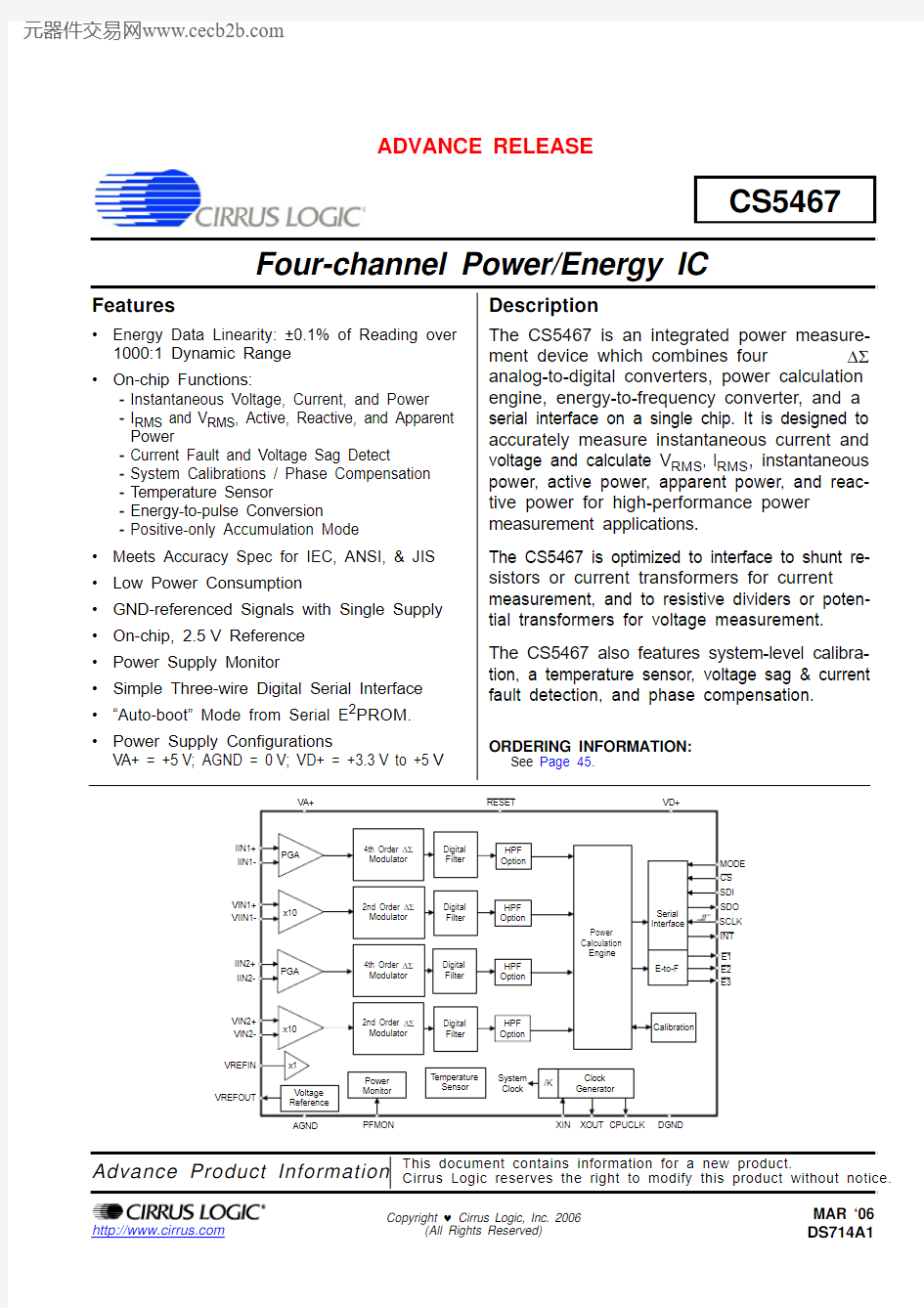
The CS5467 is a CMOS monolithic power measurement device with a computation engine and an ener-gy-to-frequency pulse output. The CS5467 combines four ?Σ analog-to-digital converters (ADCs), system calibration, and a computation engine on a single chip.
The CS5467 is designed for power measurement applications and is optimized to interface to a cur-rent-sense resistor or transformer for current measurement, and to a resistive divider or potential trans-former for voltage measurement. The current channels provide programmable gains to accommodate various input levels from a multitude of sensing elements. With a single +5V supply on VA+/AGND, the CS5467’s four input channels can accommodate common mode plus signal levels between (AGND-0.25V) and VA+.
The CS5467 also is equipped with a computation engine that calculates instantaneous power, I RMS, V RMS, apparent power, active (real) power, reactive power, and power factor. Additional features of the CS5467 include line frequency monitoring, current and voltage sag detection, zero-cross detection, pos-itive-only accumulation mode, and three programmable pulse output pins. To facilitate communication to a microprocessor, the CS5467 includes a simple three-wire serial interface which is SPI? and Microw-ire? compatible. The CS5467 provides three outputs for energy registration. Pins E1, E2, and E3 are de-signed to interface to a microprocessor.
CS5467
2. PIN DESCRIPTION
Clock Generator
Crystal Out Crystal In 1,28
XOUT, XIN - The output and input of an inverting amplifier. Oscillation occurs when connected to
a crystal, providing an on-chip system clock. Alternatively, an external clock can be supplied to
the XIN pin to provide the system clock for the device.
CPU Clock Output2CPUCLK - Output of on-chip oscillator which can drive one standard CMOS load.
Control Pins and Serial Data I/O
Serial Clock Input5SCLK - A Schmitt Trigger input pin. Clocks data from the SDI pin into the receive buffer and out of
the transmit buffer onto the SDO pin when CS is low.
Serial Data Output6SDO -Serial port data output pin.SDO is forced into a high impedance state when CS is high. Chip Select7CS - Low, activates the serial port interface.
Mode Select8MODE - High, enables the “auto-boot” mode. The mode pin is pull-down by an internal resistor.
Energy Output 22, 25,
26E3, E1, E2 - Active low pulses with an output frequency proportional to energy.
Reset23RESET - A Schmitt Trigger input pin. Low activates Reset, all internal registers (some of which
drive output pins) are set to their default states.
Interrupt24INT - Low, indicates that an enabled event has occurred.
Serial Data Input27SDI - Serial port data input pin. Data will be input at a rate determined by SCLK.
Analog Inputs/Outputs
Differential Voltage Inputs
9,10
13, 14VIN1+, VIN1-, VIN2+, VIN2- - Differential analog input pins for the voltage channel.
Differential Current Inputs 19,20,
15,16IIN+, IIN-, IIN2+, IIN2- - Differential analog input pins for the current channel.
Voltage Reference Output11VREFOUT - The on-chip voltage reference output. The voltage reference has a nominal magni-
tude of 2.5V and is referenced to the AGND pin on the converter.
Voltage Reference Input12VREFIN - The input to this pin establishes the voltage reference for the on-chip modulator. Power Supply Connections
Positive Digital Supply3VD+ - The positive digital supply.
Digital Ground4DGND - Digital Ground.
Positive Analog Supply18VA+ - The positive analog supply.
Analog Ground17AGND - Analog ground.
Power Fail Monitor 21PFMON - The power fail monitor pin monitors the analog supply. If PFMON’s voltage threshold is
tripped, a Low-Supply Detect (LSD) event is set in the status register.
CS5467
3.CHARACTERISTICS & SPECIFICATIONS
RECOMMENDED OPERATING CONDITIONS
ANALOG CHARACTERISTICS
?Min / Max characteristics and specifications are guaranteed over all Recommended Operating Conditions.?Typical characteristics and specifications are measured at nominal supply voltages and TA = 25°C.?VA+ = VD+ = 5V ±5%; AGND = DGND = 0V; VREFIN = +2.5V. All voltages with respect to 0V.?
MCLK = 4.096MHz.
Notes: 1.Applies when the HPF option is enabled.
2.Applies when the line frequency is equal to the product of the Output Word Rate (OWR) and the value
of epsilon (ε).
Parameter
Symbol Min Typ Max
Unit Positive Digital Power Supply VD+ 3.135 5.0 5.25V Positive Analog Power Supply VA+ 4.75 5.0 5.25V Voltage Reference
VREFIN - 2.5-V Specified Temperature Range
T A -40-+85
°C
Parameter
Symbol Min Typ Max Unit
Accuracy Active Power
All Gain Ranges
(Note 1)
Input Range 0.1% - 100%P Active -±0.1-%Average Reactive Power
All Gain Ranges
(Note 1 and 2)
Input Range 0.1% - 100%Q Avg -±0.2-%Power Factor
All Gain Ranges
(Note 1 and 2)
Input Range 1.0% - 100%Input Range 0.1% - 1.0%PF
--±0.2±0.27--%%Current RMS
All Gain Ranges
(Note 1)
Input Range 1.0% - 100%Input Range 0.1% - 1.0%I RMS --±0.1±0.17--%%%Voltage RMS
All Gain Ranges
(Note 1)
Input Range 5% - 100%
V RMS -±0.1-%Analog Inputs (All Channels)Common Mode Rejection (DC,50,60Hz)
CMRR
80--dB Common Mode + Signal
-0.25-VA+V Analog Inputs (Current Channels)Differential Input Range
(Gain = 10)[(IIN+) - (IIN-)]
(Gain = 50)IIN --500100--mV P-P mV P-P Total Harmonic Distortion
(Gain = 50)THD 8094-dB Crosstalk with Voltage Channel at Full Scale (50, 60Hz)
--115-dB Input Capacitance
IC -27-pF Effective Input Impedance EII
30--k ?Noise (Referred to Input)
(Gain = 10)(Gain = 50)
N I ----22.54.5μV rms μV rms Offset Drift (Without the High Pass Filter)OD - 4.0-
μV/°C Gain Error
(Note 3)
GE
-
±0.4
%
CS5467
ANALOG CHARACTERISTICS (Continued)
Notes: 3.Applies before system calibration.
4.All outputs unloaded. All inputs CMOS level.
5.Measurement method for PSRR: VREFIN tied to VREFOUT, VA+ = VD+ = 5V, a 150mV
(zero-to-peak) (60Hz) sinewave is imposed onto the +5V DC supply voltage at VA+ and VD+ pins. The “+” and “-” input pins of both input channels are shorted to AGND. The CS5464 is then commanded to continuous conversion acquisition mode, and digital output data is collected for the channel under test. The (zero-to-peak) value of the digital sinusoidal output signal is determined, and this value is converted into the (zero-to-peak) value of the sinusoidal voltage (measured in mV) that would need to be applied at the channel’s inputs, in order to cause the same digital sinusoidal output. This voltage is then defined as Veq. PSRR is (in dB):
6.When voltage level on PFMON is sagging, and LSD bit = 0, the voltage at which LSD is set to 1.
7.If the LSD bit has been set to 1 (because PFMON voltage fell below PMLO), this is the voltage level on
PFMON at which the LSD bit can be permanently reset back to 0.
Parameter
Symbol Min
Typ Max Unit Analog Inputs (Voltage Channel)Differential Input Range
[(VIN+) - (VIN-)]
VIN - 500-mV P-P Total Harmonic Distortion
THD 6575-dB Crosstalk with Current Channel at Full Scale (50, 60Hz)--70-dB Input Capacitance All Gain Ranges IC - 2.0-pF Effective Input Impedance EII 2--M ?Noise (Referred to Input)
N V --140μV rms Offset Drift (Without the High Pass Filter)OD -16.0-
μV/°C Gain Error
(Note 3)
GE -±3.0%Temperature Channel Temperature Accuracy T
-±5-°C Power Supplies
Power Supply Currents (Active State)
I A+
I D+ (VA+ = VD+ = 5V)I D+ (VA+ = 5V, VD+ = 3.3V)
PSCA PSCD PSCD --- 1.32.91.7---mA mA mA Power Consumption
Active State (VA+ = VD+ = 5V)(Note 4)
Active State (VA+ = 5V, VD+ = 3.3V)
Stand-by State Sleep State
PC
----33207103623--mW mW mW uW Power Supply Rejection Ratio (50, 60Hz)
(Note 5)
Voltage Channel
Current Channel (Gain =50x)Current Channel (Gain =10x)
PSRR 486860557565---dB dB dB PFMON Low-voltage Trigger Threshold (Note 6)PMLO 2.3 2.45-V PFMON High-voltage Power-on Trip Point (Note 7)
PMHI
- 2.55
2.7
V
PSRR 20150
V eq
---------log ?=
CS5467
VOLTAGE REFERENCE
Notes:8.The voltage at VREFOUT is measured across the temperature range. From these measurements the
9.Specified at maximum recommended output of 1μA, source or sink.
DIGITAL CHARACTERISTICS
?
Min / Max characteristics and specifications are guaranteed over all Recommended Operating Conditions.?Typical characteristics and specifications are measured at nominal supply voltages and TA = 25°C.?VA+ = VD+ = 5V ±5%; AGND = DGND = 0V. All voltages with respect to 0V.?
MCLK = 4.096MHz.
Parameter
Symbol Min Typ Max Unit Reference Output Output Voltage
VREFOUT +2.4+2.5+2.6V Temperature Coefficient (Note 8)TC VREF -2560ppm/°C Load Regulation (Note 9)
?V R
-6
10
mV
Reference Input Input Voltage Range VREFIN
+2.4+2.5+2.6V Input Capacitance -4-pF Input CVF Current
-100
-nA
Parameter
Symbol Min Typ
Max Unit Master Clock Characteristics Master Clock Frequency Internal Gate Oscillator (Note 11)
MCLK
2.5 4.09620MHz Master Clock Duty Cycle 40-60%CPUCLK Duty Cycle (Note 12 and 13)
40-60%Filter Characteristics Phase Compensation Range (Voltage Channel, 60Hz)
-2.8-+2.8°Input Sampling Rate
DCLK = MCLK/K -DCLK/8-Hz Digital Filter Output Word Rate (Both Channels)
OWR
-DCLK/1024
-Hz High-pass Filter Corner Frequency
-3dB
-0.5-Hz Full-scale DC Calibration Range (Referred to Input)(Note 14)FSCR 25
-100
%F.S.Channel-to-channel Time-shift Error (Note 15) 1.0
μs
Input/Output Characteristics High-level Input Voltage
All Pins Except XIN and SCLK and RESET
XIN
SCLK and RESET
V IH
0.6 VD+(VD+) - 0.50.8 VD+
------V V V Low-level Input Voltage (VD =5V)
All Pins Except XIN and SCLK and RESET
XIN
SCLK and RESET
V IL
---
---0.81.50.2 VD+
V V V
CS5467
Notes:10.All measurements performed under static conditions.
11.If a crystal is used, XIN frequency must remain between 2.5MHz -5.0MHz. If an external oscillator is
used, XIN frequency range is 2.5MHz -20MHz, but K must be set so that MCLK is between 2.5MHz -5.0MHz.12.If external MCLK is used, the duty cycle must be between 45% and 55% to maintain this specification.13.The frequency of CPUCLK is equal to MCLK.
14.The minimum FSCR is limited by the maximum allowed gain register value. The maximum FSCR is
limited by the full-scale signal applied to the channel input.15.Configuration Register bits PC[6:0] are set to “0000000”.
16.
The MODE pin is pulled low by an internal resistor.
Low-level Input Voltage (VD =3.3V)
All Pins Except XIN and SCLK and RESET
XIN
SCLK and RESET
V IL ------0.480.30.2 VD+
V V V High-level Output Voltage I out = +5mA
V OH (VD+) - 1.0
--V Low-level Output Voltage
I out =-5mA (VD =+5V)I out =-2.5mA (VD =+3.3V)
V OL ----0.40.4V V Input Leakage Current (Note 16)
I in -±1±10μA 3-state Leakage Current I OZ --±10μA Digital Output Pin Capacitance
C out
-
5
-pF
Parameter
Symbol Min Typ Max Unit
CS5467
SWITCHING CHARACTERISTICS
?Min / Max characteristics and specifications are guaranteed over all Recommended Operating Conditions.?Typical characteristics and specifications are measured at nominal supply voltages and TA = 25°C.?VA+ = 5V ±5% VD+ = 3.3V ±5% or 5V ±5%; AGND = DGND = 0V. All voltages with respect to 0V.?
Logic Levels: Logic 0 = 0V, Logic 1 = VD+.
Notes:17.Specified using 10% and 90% points on waveform of interest. Output loaded with 50pF.
18.Oscillator start-up time varies with crystal parameters. This specification does not apply when using an
external clock source.
Parameter
Symbol Min Typ Max Unit Rise Times (Note 17)Any Digital Output
t rise ---50 1.0-μs ns Fall Times (Note 17)Any Digital Output
t fall
---50 1.0-μs ns Start-up
Oscillator Start-up Time XTAL = 4.096MHz (Note 18)
t ost -60-ms Serial Port Timing Serial Clock Frequency SCLK --2MHz Serial Clock Pulse Width High Pulse Width Low
t 1t 2200200
--
--
ns ns
SDI Timing
CS Falling to SCLK Rising
t 350--ns Data Set-up Time Prior to SCLK Rising t 450--ns Data Hold Time After SCLK Rising t 5100--ns SDO Timing
CS Falling to SDO Driving
t 6-2050ns SCLK Falling to New Data Bit (hold time)t 7-2050ns CS Rising to SDO Hi-Z t 8-
2050
ns Auto-Boot Timing Serial Clock
Pulse Width Low Pulse Width High t 9t 1088
MCLK MCLK MODE setup time to RESET Rising t 1150ns RESET rising to CS falling t 1248MCLK
CS falling to SCLK rising t 13100
8MCLK SCLK falling to CS rising
t 1416
MCLK CS rising to driving MODE low (to end auto-boot sequence)t 1550ns SDO guaranteed setup time to SCLK rising
t 16
100
ns
CS5467
Figure 1. CS5464 Read and Write Timing Diagrams
CS5467
SWITCHING CHARACTERISTICS (Continued)
Notes:19.Pulse output timing is specified at MCLK =4.096MHz, E2MODE =0, and E3MODE[1:0]=0. Refer to
5.5 Energy Pulse Output on page 18 for more information on pulse output pins.20.Timing is proportional to the frequency of MCLK.
ABSOLUTE MAXIMUM RATINGS
WARNING:Operation at or beyond these limits may result in permanent damage to the device.
Normal operation is not guaranteed at these extremes .
Notes:21.VA+ and AGND must satisfy [(VA+) - (AGND)] ≤ + 6.0V.
22.VD+ and AGND must satisfy [(VD+) - (AGND)] ≤ + 6.0V.
23.Applies to all pins including continuous over-voltage conditions at the analog input pins.24.Transient current of up to 100mA will not cause SCR latch-up.25.Maximum DC input current for a power supply pin is ±50mA.
26.Total power dissipation, including all input currents and output currents.
Parameter
Symbol Min Typ Max Unit E1, E2, and E3 Timing (Note 19 and 20)
Period t period 250--μs Pulse Width
t pw 244--μs Rising Edge to Falling Edge
t 36--μs E2 Setup to E1 and/or E3 Falling Edge t 4 1.5--μs E1 Falling Edge to E3 Falling Edge
t 5
248
-
-
μs
Parameter
Symbol Min Typ Max Unit DC Power Supplies
(Notes 21 and 22)Positive Digital Positive Analog VD+VA+-0.3-0.3--+6.0+6.0V V Input Current, Any Pin Except Supplies (Notes 23, 24, 25)
I IN --±10mA Output Current, Any Pin Except VREFOUT I OUT
--100mA Power Dissipation (Note 26)P D --500mW Analog Input Voltage All Analog Pins V INA - 0.3-(VA+) + 0.3V Digital Input Voltage
All Digital Pins
V IND -0.3-(VD+) + 0.3
V Ambient Operating Temperature T A -40-85°C Storage Temperature
T stg
-65
-
150
°C
Figure 2. Timing Diagram for E1, E2, and E3
CS5467
4.THEORY OF OPERATION
The CS5467 is a four-channel analog-to-digital convert-er (ADC) followed by a computation engine that per-forms power calculations and energy-to-pulse conversion. The data flow for the voltage and current channel measurement and the power calculation algo-rithms are depicted in Figures 3, 4, and 5.
The CS5467 analog inputs are structured with two Cur-rent channels and two Voltage channels, and are opti-mized to simplify interfacing to various sensing elements. As shown in Figures 3 and 4, the current and voltage channels are fully independent.
The voltage-sensing elements introduces a voltage waveform on the two voltage channel inputs VIN± and VIN2±, which is subject to a gain of 10x. A second-order delta-sigma modulator samples the amplified signal for digitization.
Simultaneously, the current-sensing elements introduce a voltage waveform on the two current channel inputs IIN± and IIN2±, which is subject to the two selectable gains of the programmable gain amplifier (PGA). The amplified signals are sampled by a fourth-order delta-sigma modulator for digitization. The converters sample at a rate of MCLK/8. The over-sampling pro-vides a wide dynamic range and simplified anti-alias fil-ter design.
4.1 Digital Filters
The decimating digital filters on the four channels are Sinc3 filters followed by 3rd-order IIR filters. The sin-gle-bit data is passed to the low-pass decimation filter and output at a fixed word rate. The output word is passed to an IIR filter to compensate for the magnitude roll off of the low-pass filtering operation.
An optional digital high-pass filter (HPF in Figures 3 and 4) removes any DC component from the selected signal path. By removing the DC component from the voltage and/or the current channel, any DC content will also be removed from the calculated active power as well. With both HPFs enabled the DC component will be removed
Figure 3. Data Measurement Flow Diagram
Figure 4. Data Measurement Flow Diagram
CS5467
from the calculated V RMS and I RMS , as well as the ap-parent power.
When the optional HPF in either channel is disabled, an all-pass filter (APF) in the complementary channel is im-plemented. The APF has an amplitude response that is flat within the channel bandwidth and is used for match-ing phase in systems where only one channel’s HPF is engaged.
4.2 Voltage and Current Measurements
The digital filter output word is subject to a DC-offset ad-justment and a gain calibration (See Section 7. System Calibration on page 39). The calibrated measurement is available by reading the instantaneous voltage and cur-rent registers.
The Root Mean Square (RMS in Figure 5) calculations are performed on N instantaneous voltage and current samples, V n and I n , respectively (where N is the cycle count), using the formula:
and likewise for V RMS , using V n . I RMS and V RMS are ac-cessible by register reads, which are updated once ev-ery cycle count (referred to as a computational cycle).
4.3 Power Measurements
The instantaneous voltage and current samples are multiplied to obtain the instantaneous power (see Fig-ure 3 and 4). The product is then averaged over N con-versions to compute active power. The average active power measured on channels 1 and 2 is used to drive energy pulse output E1. Energy output E2 is config-urable and can provide an energy sign or a pulse output that is proportional to the average apparent power mea-sured on channels 1 and 2. Energy output E3 provides a pulse output that is proportional to the average reac-tive power or the average apparent power measured on channels 1 and 2. Output E3 can also be set to indicate the PFMON comparator output or to indicate the sign of the voltage applied to the voltage channel.
The apparent power (S, S2) is the combination of the active power and reactive power, without reference to an impedance phase angle, and is calculated by the CS5467 using the following formula:
Power Factor (PF, PF2) is the active power (P Active ,P2Active ) divided by the apparent power (S, S2)
The sign of the power factor is determined by the active power.
I RMS I n
n 0=N 1
–∑
N
--------------------=
Figure 5. Power Calculation Flow
S V RMS I RMS
×=PF P Active
S
------------------=
CS5467
The CS5467 calculates the reactive power (Q Trig ,Q2Trig ) utilizing trigonometric identities, using the formu-la
The average reactive power calculation (Q Avg , Q2Avg ) is
generated by averaging the voltage and multiplying that value by the current measurement with a 90° phase dif-ference between the two. The 90° phase shift is realized by applying an IIR digital filter in the voltage channel to obtain quadrature voltage (see Figure 3 and 4). This fil-ter will give exactly -90° phase shift across all frequen-cies, and utilizes epsilon (ε) to achieve unity gain at the line frequency.
The instantaneous quadrature voltage (V Q , V2Q ) and current (I, I2) samples are multiplied to obtain the in-stantaneous quadrature power (Q, Q2). The product is then averaged over N conversions, utilizing the formula
The peak current (I peak , I2peak ) and peak voltage (V peak ,V2peak ) are the instantaneous current and voltage, re-spectively, with the greatest magnitude detected during the previous computation cycle. Active, apparent, reac-tive, and fundamental power are updated every compu-tation cycle.
4.4 Linearity Performance
The linearity of the V RMS , I RMS , active, reactive, and power-factor power measurements (before calibration)will be within ±0.1% of reading over the ranges speci-fied, with respect to the input voltage levels required to cause full-scale readings in the I RMS and V RMS regis-ters. Refer to Accuracy Specifications on page 7.Until the CS5467 is calibrated, the accuracy of the CS5467 (with respect to a reference line-voltage and line-current level on the power mains) is not guaranteed
Q Trig S 2
P Active
2–
=
Q Avg
Q n
n 1
=N
∑N
------------------------=
CS5467
5.FUNCTIONAL DESCRIPTION
5.1 Analog Inputs
The CS5467 is equipped with four fully differential input channels. The inputs VIN ±, VIN2±, IIN ±, and IIN2± are designated as the voltage, voltage 2, current, and cur-rent 2 channel inputs, respectively. The full-scale differ-ential input voltage for the current and voltage channel is ±250mV P .
5.1.1 Voltage Channel Input
The output of the line voltage resistive divider or trans-former is connected to the VIN+ (VIN2+) and VIN-(VIN2-) input pins of the CS5467. The voltage channels are equipped with a 10x fixed-gain amplifier. The full-scale signal level that can be applied to the voltage channel is ±250mV. If the input signal is a sine wave,the maximum RMS voltage at a gain 10x is:
which is approximately 70.7% of maximum peak volt-age. The voltage channel is also equipped with a Volt-age Gain Register , allowing for an additional programmable gain of up to 4x.
5.1.2 Current Channel Inputs
The output of the current-sense resistor or transformer is connected to the IIN+ (IIN2+) and IIN- (IIN2-) input pins of the CS5467. To accommodate different cur-rent-sensing elements, the current channel incorpo-rates a programmable gain amplifier (PGA) with two programmable input gains. Configuration Register bit Igain (I2gain) defines the two gain selections and corre-sponding maximum input signal level.
For example, if Igain=0 (I2gain=0), current channel 1(2)PGA gain is set to 10x. If the input signals are pure si-nusoids with zero phase shift, the maximum peak differ-ential signal on the current or voltage channel is ±250mV P . The input signal levels are approximately 70.7% of maximum peak voltage and produce a full-scale energy pulse registration equal to 50% of ab-solute maximum energy registration. This will be dis-cussed further in See Section 5.5 Energy Pulse Output on page 18.
The Current Gain Register also facilitates an additional programmable gain of up to 4x. If an additional gain is applied to the voltage and/or current channel, the maxi-mum input range should be adjusted accordingly.
5.2 IIR Filters
The current and voltage channels are equipped with a 3rd-order IIR filter, that is used to compensate for the magnitude roll off of the low-pass decimation filter.
5.3 High-pass Filters
By removing the offset from either channel, no error component will be generated at DC when computing the active power. By removing the offset from both chan-nels, no error component will be generated at DC when computing V RMS , I RMS , and apparent power. Operation-al Mode Register bits VHPF, VHPF2, IHPF and IHPF2activate the HPF in the voltage and current channel, re-spectively. When a high-pass filter is active in only one channel, an all-pass filter (APF) is applied to the com-panion channel. The APF has an amplitude response that is flat within the channel bandwidth and is used for matching phase in systems where only one HPF is en-gaged.
5.4 Performing Measurements
The CS5467 performs measurements of instantaneous voltage (V n ) and current (I n ), and calculates instanta-neous power (P n ) at an output word rate (OWR) of
where K is the value of the clock divider selected in the Configuration Register by bits K[3:0]. Note that a value of K[3:0]=0000 results in a clock divider setting of 16,rather than zero.
The RMS voltage (V RMS , V2RMS ), RMS current (I RMS ,I2RMS ), and active power (P active , P2active ) are comput-ed using N instantaneous samples of V n , I n , and P n re-spectively, where N is the value in the Cycle Count Register and is referred to as a “computation cycle ”. The apparent power (S, S2) is the product of V RMS and I RMS .A computation cycle is derived from the master clock (MCLK), with frequency: Under default conditions and
with K =1, N =4000, and MCLK =4.096MHz – the OWR =4000 and the Computation Cycle = 1Hz.
Igain, I2gain
Maximum Input
Gain
0±250mV 10x 1
±50mV
50x
Table 1. Current Channel PGA Setting
250mV P
2
--------------------176.78mV
RMS
?OWR MCLK K ?()
1024
----------------------------= Computation Cycle OWR
N
---------------=
CS5467
All measurements are available as a percentage of full scale. The format for signed registers is a two’s comple-ment, normalized value between -1 and +1. The format for unsigned registers is a normalized value between 0 and 1. A register value of
represents the maximum possible value.
At each instantaneous measurement, the CRDY bit will be set in the Status Register, and the INT pin will be-come active if the CRDY bit is unmasked in the Mask Register. At the end of each computation cycle, the DRDY bit will be set in the Status Register, and the INT pin will become active if the DRDY bit is unmasked in the Mask Register. When these bits are asserted, they must be cleared before they can be asserted again.
If the Cycle Count Register (N) is set to 1, all output cal-culations are instantaneous, and DRDY, like CRDY, will indicate when instantaneous measurements are fin-ished. Some calculations are inhibited when the cycle count is less than 2.
Epsilon (ε) is the ratio of the input line frequency (f i) to the sample frequency (f s) of the ADC.
where f s=MCLK/(K x 1024). With MCLK=4.096MHz and clock divider K=1, f s=4000Hz. For the two most-common line frequencies, 50Hz and 60Hz
and
respectively. Epsilon is used to set the gain of the 90°phase shift (IIR) filter for the average reactive power cal-culation.
5.5 Energy Pulse Output
The CS5467 provides three output pins for energy reg-istration. By default, E1 is used to register average ac-tive energy measured on channels 1 and 2, E3 is used to register average reactive energy measured on chan-nels 1 and 2, and E2 indicates the sign of both active and reactive energy. (See Figure 2. Timing Diagram for E1, E2, and E3 on page 13.) The E1 pulse output is designed to indicate the average active energy measured on channels 1 and 2. The E2 pin can be used to register average apparent energy measured on channels 1 and 2 or to indicate the sign of energy. Table2 defines the pulse output mode, which is controlled by bit E2MODE in the Operational Mode Reg-ister.
The E3 pin can be set to register average reactive ener-gy measured on channels 1 and 2 (default), PFMON, voltage channel sign, or average apparent energy mea-sured on channels 1 and 2. Table3 defines the pulse output format, which is controlled by bits E3MODE[1:0] in the Operational Mode Register.
The pulse output frequencies of E1, E2, and E3 are di-rectly proportional to the power calculated from the input signals. The value contained in the PulseRateE Regis-ter is the ratio of the frequency of energy-output pulses to the number of samples, at full scale, which defines the average frequency for the output pulses. The pulse width, t pw in Figure 2, is an integer multiple of MCLK cy-cles approximately equal to:
If MCLK=4.096MHz and K=1 then t pw?0.25ms. 5.5.1 Active Energy
The E1 pin produces active-low pulses with an output frequency proportional to the average active power measured on channels 1 and 2. The E2 pin is the ener-gy direction indicator. Positive energy is represented by E1 pin falling while the E2 is high. Negative energy is represented by the E1 pin falling while the E2 is low. The E1 and E2 switching characteristics are specified in Figure 2. Timing Diagram for E1, E2, and E3 on page 13.
223
1
–
()
223
-----------------------0.99999988
=
εf i f s?=
ε50Hz4000Hz
?0.0125 ==
ε60Hz4000Hz
?0.015 ==
E2MODE E2 Output Mode
0Sign of Energy
1Apparent Energy
Table 2. E2 Pin Configuration
E3MODE1E3MODE0E3 OutPut Mode 00Reactive Energy
01PFMON
10Voltage Channel Sign 11Apparent Energy Table 3. E3 Pin Configuration
t pw sec
()
1
( MCLK/K ) / 1024
------------------------------------
?
CS5467
Figure 6 illustrates the pulse output format with positive active energy and negative reactive energy.
The pulse output frequency of E1 is directly proportional to the active power calculated from the input signals. To calculate the output frequency of E1, the following trans-fer function can be utilized:
With MCLK =4.096MHz, PF = 1, and default settings,the pulses will have an average frequency equal to the frequency specified by PulseRateE when the input sig-nals applied to the voltage and current channels cause full-scale readings in the instantaneous voltage and cur-rent registers. The maximum pulse frequency from the E1 pin is (MCLK/K)/2048.
5.5.2 Apparent Energy Mode
Pin E2 outputs apparent energy pulses when the Oper-ational Mode Register bit E2MODE =1. Pin E3 outputs apparent energy pulses when the Operational Mode Register bits E3MODE[1:0]=3 (11b). Figure 7 illus-trates the pulse output format with apparent energy on E2 (E2MODE =1 and E3MODE[1:0]=0)
The pulse output frequency of E2 (and/or E3) is directly proportional to the apparent power calculated from the input signals. Since apparent power is without reference to an impedance phase angle, the following transfer function can be utilized to calculate the output frequency on E2 (and/or E3).
With MCLK =4.096MHz and default settings, the puls-es will have an average frequency equal to the frequen-cy specified by PulseRateE when the input signals applied to the voltage and current channels cause full-scale readings in the instantaneous voltage and cur-rent registers. The maximum pulse frequency from the E2 (and/or E3) pin is (MCLK/K)/2048. The E2 (and/or E3) pin outputs apparent energy, but has no energy di-rection indicator.
5.5.3 Reactive Energy Mode
Reactive energy pulses are output on pin E3 by setting bit E3MODE[1:0]=0 (default) in the Operational Mode Register . Positive reactive energy is registered by E3falling when E2 is high. Negative reactive energy is reg-istered by E3 falling when E2 is low. Figure 6 on page 19 illustrates the pulse output format with negative reactive energy output on pin E3 and the sign of the en-ergy on E2. The E3 and E2 pulse output switching char-acteristics are specified in Figure 2 on page 13.The pulse output frequency of E3 is directly proportional to the reactive power calculated from the input signals.To calculate the output frequency on E3, the following transfer function can be utilized:With MCLK =4.096MHz, PF = 0 and default settings,the pulses will have an average frequency equal to the frequency specified by PulseRateE when the input sig-nals applied to the voltage and current channels cause full-scale readings in the instantaneous voltage and cur-
Figure 6. Active and Reactive energy pulse outputs
where
FREQ P = Average frequency of active energy E1 pulses [Hz]VIN(2) = rms voltage across VIN(2)+ and VIN(2)- [V]V(2)gain = Voltage channel gain
IIN(2) = rms voltage across IIN(2)+ and IIN(2)- [V]I(2)gain = Current channel gain PF(2) = Power Factor
PulseRate = PulseRateE x (MCLK/K)/2048 [Hz]VREFIN = Voltage at VREFIN pin [V]
FREQ P P Active P2Active +()2?[]PulseRate
×=P 2()Active
VIN 2()V 2()gain ×IIN 2()×I 2()gain ×PF 2()×VREFIN
2
----------------------------------------------------------------------------------------------------------------------------------
-=
Figure 7. Apparent energy pulse outputs
where
FREQ S = Average frequency of apparent energy E2 and/or E3 pulses [Hz]VIN(2) = rms voltage across VIN(2)+ and VIN(2)- [V]V(2)gain = Voltage channel gain
IIN(2) = rms voltage across IIN(2)+ and IIN(2)- [V]I(2)gain = Current channel gain
PulseRate = PulseRateE x (MCLK/K)/2048 [Hz]VREFIN = Voltage at VREFIN pin [V]
FREQ
S
S S2+()2?[]PulseRate
×=S 2()
VIN 2()V 2()gain ×IIN 2()×I 2()gain ×VREFIN
2
----------------------------------------------------------------------------------------------------------=
where
FREQ Q = Average frequency of reactive energy E3 pulses [Hz]VIN(2) = rms voltage across VIN(2)+ and VIN(2)- [V]V(2)gain = Voltage channel gain
IIN(2) = rms voltage across IIN(2)+ and IIN(2)- [V]I(2)gain = Current channel gain
PQ = PulseRate = PulseRateE x (MCLK/K)/2048 [Hz]VREFIN = Voltage at VREFIN pin [V]
FREQ Q Q Avg Q2Avg +()2?[]PulseRate
×=Q 2()Avg
VIN 2()V 2()gain ×IIN 2()×I 2()gain ×PQ 2()×VREFIN
2
------------------------------------------------------------------------------------------------------------------------------------=
1PF 2
–
CS5467
rent registers. The maximum pulse frequency from the E1 pin is (MCLK/K)/2048.
5.5.4 Voltage Channel Sign Mode
Setting bits E3MODE[1:0]=2 (10b) in the Operational Mode Register outputs the sign of the voltage channel on pin E3. Figure 8 illustrates the output format with volt-age channel sign on E3
Output pin E3 is high when the line voltage is positive and pin E3 is low when the line voltage is negative. 5.5.5 PFMON Output Mode
Setting bit E3MODE[1:0]=1 (01b) in the Operational Mode Register outputs the state of the PFMON compar-ator on pin E3. Figure 9 illustrates the output format with PFMON on E3
When PFMON is greater than the threshold, pin E3 is high and when PFMON is less than the threshold pin E3 is low.
5.6 Sag and Fault Detect Feature
Status bit VSAG (V2SAG) and IFAULT (I2FAULT) in the Status Register, indicates a sag occurred in the power line voltage (voltage 2) and current (current 2), respec-tively. For a sag condition to be identified, the absolute value of the instantaneous voltage or current must be less than the sag level for more than half of the sag du-ration (see Figure 10).
To activate voltage sag detection, a voltage sag level must be specified in the Voltage Sag Level Register (VSAG level, V2SAG level), and a voltage sag duration must be specified in the Voltage Sag Duration Register (VSAG duration, V2SAG duration). To activate current fault detection, a current sag level must be specified in the Current Fault Level Register (ISAG level, I2SAG level), and a current sag duration must be specified in the Current Fault Duration Register (ISAG duration, I2SAG duration). The voltage and current sag levels are specified as the average of the absolute instantaneous voltage and cur-rent, respectively. Voltage and current sag duration is
5.7 On-chip Temperature Sensor
The on-chip temperature sensor is designed to assist in
characterizing the measurement element over a desired
temperature range. Once a temperature characteriza-
tion is performed, the temperature sensor can be uti-
lized to assist in compensating for temperature drift.
Temperature measurements are performed when a one
is written to the Temperature Measurement (T meas) reg-
ister and stored in the Temperature Register. The Tem-
perature Register (T) default is Celsius scale (°C). The
Temperature Gain Register (T gain) and Temperature
Offset Register (T off) are constant values allowing for
temperature scale conversions.
The temperature update rate is a function of the number
of ADC samples. With MCLK=4.096MHz and K=1
the update rate is:
The Cycle Count Register (N) must be set to a value
greater than one. Status bit TUP in the Status Register,
indicates when the Temperature Register is updated.
The Temperature Offset Register sets the zero-degree
measurement. To improve temperature measurement
accuracy, the zero-degree offset may need to be adjust-
ed after the CS5467 is initialized. Temperature-offset
calibration is achieved by adjusting the Temperature
Offset Register (T off) by the differential temperature
(?T) measured from a calibrated digital thermometer
and the CS5467 temperature sensor. A one-degree ad-
justment to the Temperature Register (T) is achieved by Figure 8. Voltage Channel Sign Pulse outputs
2240 samples
MCLK K
?
()1024
?
---------------------------------------0.56 sec
=