BC237, BC237B, BC237C, BC239C
Amplifier Transistors
NPN Silicon
Features
?Pb?Free Packages are Available*
MAXIMUM RATINGS
Rating Symbol Value Unit
Collector?Emitter Voltage
BC237
BC239V CEO
45
25
Vdc
Collector?Emitter Voltage
BC237
BC239V CES
50
30
Vdc
Collector?Emitter Voltage
BC237
BC239V EBO
6.0
5.0
Vdc
Collector Current ? Continuous I C100mAdc
Total Power Dissipation @ T A = 25°C Derate above T A = 25°C P D350
2.8
mW
mW/°C
Total Power Dissipation @ T A = 25°C Derate above T A = 25°C P D 1.0
8.0
W
mW/°C
Operating and Storage Temperature
Range
T J, T stg?55 to +150°C THERMAL CHARACTERISTICS
Characteristic Symbol Max Unit Thermal Resistance, Junction?to?Ambient R q JA357°C/W
Thermal Resistance, Junction?to?Case R q JC125°C/W Maximum ratings are those values beyond which device damage can occur. Maximum ratings applied to the device are individual stress limit values (not normal operating conditions) and are not valid simultaneously. If these limits are exceeded, device functional operation is not implied, damage may occur and reliability may be affected.
*For additional information on our Pb?Free strategy and soldering details, please download the ON Semiconductor Soldering and Mounting Techniques Reference Manual, SOLDERRM/D.
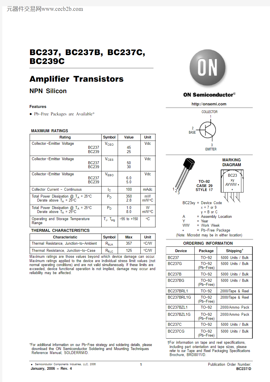
Device Package Shipping?
ORDERING INFORMATION
BC237TO?925000 Units / Bulk BC23xy=Device Code
x = 7 or 9
y = B or C
A=Assembly Location
Y=Year
WW=Work Week
G=Pb?Free Package
MARKING
DIAGRAM
TO?92
CASE 29
STYLE 17
12
BC237B TO?925000 Units / Bulk BC237G TO?92
(Pb?Free)
5000 Units / Bulk
BC237BG TO?92
(Pb?Free)
5000 Units / Bulk (Note: Microdot may be in either location)
https://www.doczj.com/doc/6f10065140.html,
BC23
xy
AYWW G
G
COLLECTOR
1
2
BASE
3
EMITTER
BC237BRL1TO?922000/Tape & Reel BC237BZL1TO?922000/Ammo Pack BC237BRL1G TO?92
(Pb?Free)
2000/Tape & Reel
BC237BZL1G TO?92
(Pb?Free)
2000/Ammo Pack BC237C TO?925000 Units / Bulk
BC237CG TO?92
(Pb?Free)
5000 Units / Bulk
?For information on tape and reel specifications, including part orientation and tape sizes, please refer to our T ape and Reel Packaging Specifications Brochure, BRD8011/D.
ELECTRICAL CHARACTERISTICS (T A = 25°C unless otherwise noted)
Characteristic Symbol Min Typ Max Unit OFF CHARACTERISTICS
Collector?Emitter Breakdown Voltage BC237
(I C = 2.0 mA, I B = 0)BC239V(BR)CEO45
25
?
?
?
?
V
Emitter?Base Breakdown Voltage BC237
(I E = 100 m A, I C = 0)BC239V(BR)EBO 6.0
5.0
?
?
?
?
V
Collector Cutoff Current
(V CE = 30 V, V BE = 0)BC239 (V CE = 50 V, V BE = 0)BC237 (V CE = 30 V, V BE = 0) T A = 125°C BC239 (V CE = 50 V, V BE = 0) T A = 125°C BC237I CES
?
?
?
?
0.2
0.2
0.2
0.2
15
15
4.0
4.0
nA
m A
ON CHARACTERISTICS
DC Current Gain
(I C = 10 m A, V CE = 5.0 V)BC237B
BC237C/239C
(I C = 2.0 mA, V CE = 5.0 V)BC237
BC237B
BC237C/239C
(I C = 100 mA, V CE = 5.0 V)BC237B
BC237C/239C h FE
?
?
120
200
380
?
?
150
270
?
290
500
180
300
?
?
800
460
800
?
?
?
Collector?Emitter On Voltage
(I C = 10 mA, I B = 0.5 mA)BC237/BC239
(I C = 100 mA, I B = 5.0 mA)BC237/BC239V CE(sat)
?
?
0.07
0.2
0.2
0.6
V
Base?Emitter Saturation Voltage
(I C = 10 mA, I B = 0.5 mA)
(I C = 100 mA, I B = 5.0 mA)V BE(sat)
?
?
0.6
?
0.83
1.05
V
Base?Emitter On Voltage
(I C = 100 m A, V CE = 5.0 V)
(I C = 2.0 mA, V CE = 5.0 V)
(I C = 100 mA, V CE = 5.0 V)V BE(on)
?
0.55
?
0.5
0.62
0.83
?
0.7
?
V
DYNAMIC CHARACTERISTICS
Current?Gain — Bandwidth Product
(I C = 0.5 mA, V CE = 3.0 V, f = 100 MHz)BC237
BC239
(I C = 10 mA, V CE = 5.0 V, f = 100 MHz)BC237
BC239f T
?
?
150
150
100
140
200
280
?
?
?
?
MHz
Collector?Base Capacitance
(V CB = 10 V, I C = 0, f = 1.0 MHz)
C obo?? 4.5pF
Emitter?Base Capacitance
(V EB = 0.5 V, I C = 0, f = 1.0 MHz)
C ibo?8.0?pF
Noise Figure
(I C = 0.2 mA, V CE = 5.0 V, R S = 2.0 k W, f = 1.0 kHz)BC239
(I C = 0.2 mA, V CE = 5.0 V, R S = 2.0 k W, f = 1.0 kHz, D f = 200 Hz)BC237
BC239NF
?
?
?
2.0
2.0
2.0
4.0
10
4.0
dB
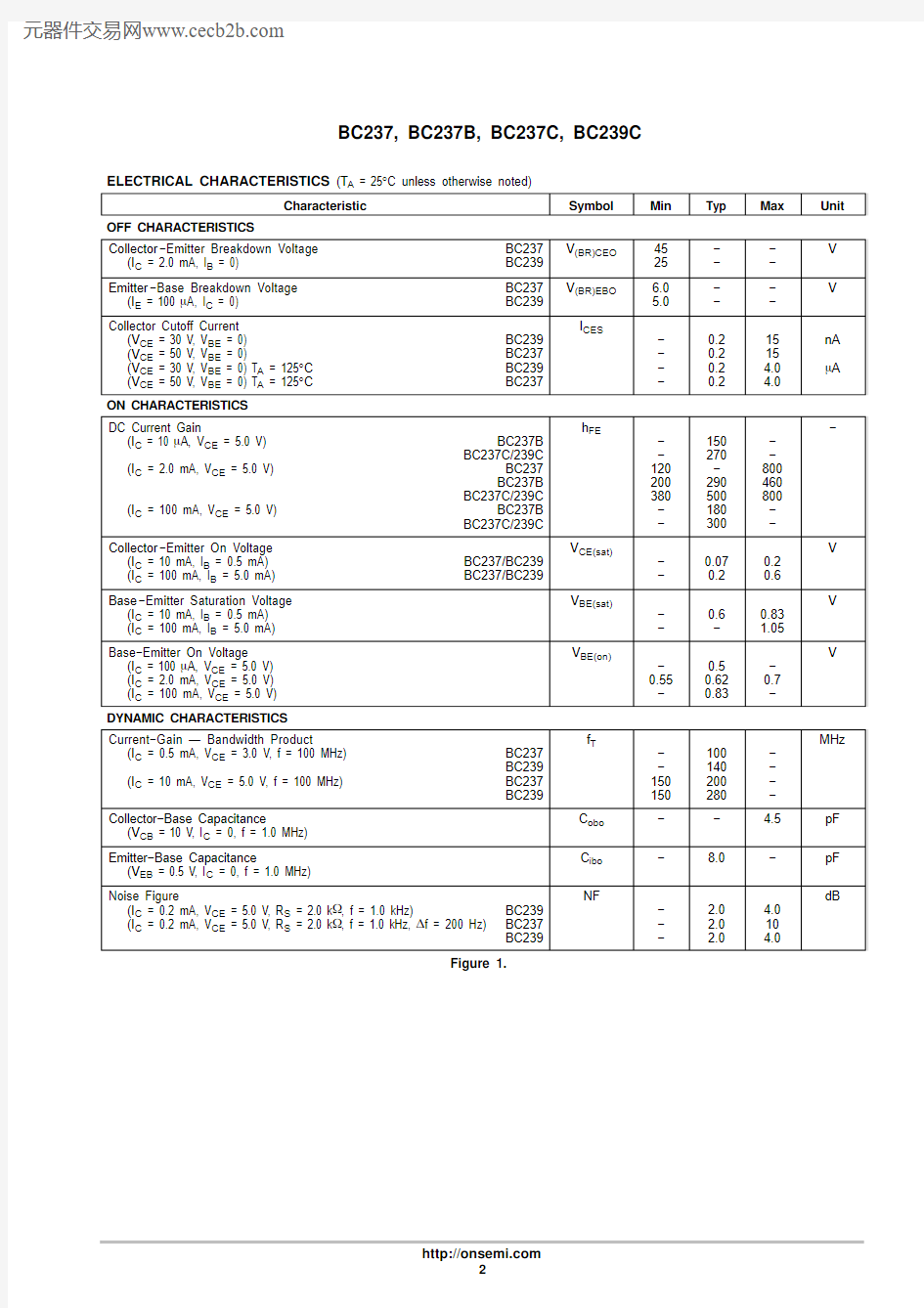
Figure 1.
2.01.51.00.20.30.40.60.8
I C , COLLECTOR CURRENT (mAdc)
Figure 1. Normalized DC Current Gain
h F E , N O R M A L I Z E D D C C U R R E N T G A I N
1.00.90.80.70.60.50.40.30.20.1
I C , COLLECTOR CURRENT (mAdc)
Figure 2. “Saturation” and “On” Voltages
V , V O L T A G E (V O L T S )
40020
30406080100200
300
I C
, COLLECTOR CURRENT (mAdc)
Figure 3. Current?Gain — Bandwidth Product f T , C U R R E N T ?G A I N ? B A N D W I D T H P R O D U C T (M H z )
C , C A P A C I T A N
C E (p F )
101.02.0
3.05.0
7.0V R , REVERSE VOLTAGE (VOLTS)
Figure 4. Capacitances
r b , B A S E S P R E A D I N G R E S I S T A N C E (O H M S )
170160150140130120I C , COLLECTOR CURRENT (mAdc)
Figure 5. Base Spreading Resistance
PACKAGE DIMENSIONS
NOTES:
1.DIMENSIONING AND TOLERANCING PER ANSI Y14.5M, 198
2.
2.CONTROLLING DIMENSION: INCH.
3.CONTOUR OF PACKAGE BEYOND DIMENSION R IS UNCONTROLLED.
4.LEAD DIMENSION IS UNCONTROLLED IN P AND BEYOND DIMENSION K MINIMUM.
PLANE
DIM
MIN MAX MIN MAX MILLIMETERS
INCHES A 0.1750.205 4.45 5.20B 0.1700.210 4.32 5.33C 0.1250.165 3.18 4.19D 0.0160.0210.4070.533G 0.0450.055 1.15 1.39H 0.0950.105 2.42 2.66J 0.0150.0200.390.50K 0.500???12.70???L 0.250??? 6.35???N 0.0800.105 2.04 2.66P ???0.100??? 2.54R 0.115??? 2.93???V
0.135???
3.43???
TO?92 (TO?226)CASE 29?11ISSUE AL
STYLE 17:
PIN 1.COLLECTOR
2.BASE
3.EMITTER
ON Semiconductor and are registered trademarks of Semiconductor Components Industries, LLC (SCILLC). SCILLC reserves the right to make changes without further notice to any products herein. SCILLC makes no warranty, representation or guarantee regarding the suitability of its products for any particular purpose, nor does SCILLC assume any liability arising out of the application or use of any product or circuit, and specifically disclaims any and all liability, including without limitation special, consequential or incidental damages.“Typical” parameters which may be provided in SCILLC data sheets and/or specifications can and do vary in different applications and actual performance may vary over time. All operating parameters, including “Typicals” must be validated for each customer application by customer’s technical experts. SCILLC does not convey any license under its patent rights nor the rights of others. SCILLC products are not designed, intended, or authorized for use as components in systems intended for surgical implant into the body, or other applications intended to support or sustain life, or for any other application in which the failure of the SCILLC product could create a situation where personal injury or death may occur. Should Buyer purchase or use SCILLC products for any such unintended or unauthorized application, Buyer shall indemnify and hold SCILLC and its officers, employees, subsidiaries, affiliates,and distributors harmless against all claims, costs, damages, and expenses, and reasonable attorney fees arising out of, directly or indirectly, any claim of personal injury or death associated with such unintended or unauthorized use, even if such claim alleges that SCILLC was negligent regarding the design or manufacture of the part. SCILLC is an Equal Opportunity/Affirmative Action Employer. This literature is subject to all applicable copyright laws and is not for resale in any manner.
PUBLICATION ORDERING INFORMATION