250mA Ultra Low Drop Out Regulator With High Slew Rate Double Recycling Folded Cascode Error
Amplifier
Sreehari Rao Patri1, Suresh Alapati 2, Surendra Chowdary3 , Krishna Prasad4
1,2,3Department of Electronics and Communication Engineering
1,2,3National Institute of Technology Warangal, Warangal-506004, Andhra Pradesh, India.
1patri@nitw.ac.in,2suresh_nitw@nitw.ac.in,3surendra0292@https://www.doczj.com/doc/637285056.html,,4krish@nitw.ac.in
Abstract—This paper presents a modified folded cascode error amplifier of low dropout (LDO) regulator and a compensation scheme to improve the transient response. The proposed error amplifier enhances its transconductance, gain, and slew rate by recycling the shunt current sources of conventional folded cascode amplifier without increasing area or power consumption. The design is implemented in a standard UMC 0.18μm CMOS process. The LDO regulator consumes a quiescent current of 34μAonly. Simulation results show that the overshoot/undershoot in the output voltage under the extreme load transients are 177.7mV/139mV for load current range of 0.5mA to 250mA with an output capacitor of 1pF. The LDO presented is useful for chip level power management suitable for SoC applications.
Keywords—high load current, low-dropout voltage regulator, double recycling folded cascode error amplifier, low-quiescent current.
I.I NTRODUCTION
Power management is indispensable for portable electronic devices and embedded systems. The portable applications demands for low voltage, low power, low standby current, less silicon area and pin count to make them possible to be implemented on system-on-chip (SoC) is increasing. It features a high level of integration and enables mobile applications devices to be cost-effective, thinner, and compact with better power efficiency [1].
Low drop out regulators (LDO) are an essential part of the power management system that provides constant voltage supply with improved power efficiency and fast transient response i.e. they should be capable of responding quickly to changes in load current. Power efficiency of LDO can be improved by reducing the quiescent current and drop out voltage. However, it unavoidably slows down the transient response of an LDO regulator. The performance determining parameters of LDO are greatly influenced by the positive and negative load dumps at the output of LDO. In past, several techniques are proposed for improving transient response time, transient voltage variations at the output and power efficiency in order to maintain a reliable supply voltage for SoC applications. In order to make the transition to fully integrated LDOs, the traditional structure is explored and modified in the error amplifier, the addition of some extra block ,or some combination of both to achieve the required performance[2]. Regarding the error amplifier, the error amplifier variations include: class AB structure[3], operational transconductance amplifier[4],and flipped voltage follower[5],while,the modifications for overall structure of LDO include: Active feedback compensation[6], hybrid cascode compensation[7], and dynamic Biasing[8].In [3], the well known class AB amplifier reduces the pass transistor gate parasitic capacitance charging time, thus, improving the transient response, while the very complex structure reduces error amplifier bandwidth for reaching good stability. In[4], two-stage cascode operational transconductance amplifier (OTA) as error amplifier is used and OTAs are the best components to drive the capacitive loads because of the fact that their output signal is a current controlled by a differential input signal. In [5] although proposed structure shows a good load and line regulations and quiescent power consumption is constant independent of load, but occupies a larger silicon area of 0.7mm2and not suitable for SoC. In [6], the adaptive output stage circuit is proposed to deliver extra four times of output current to the operational amplif er at medium to heavy loads to extend the bandwidth of the LDO and enhance the slew rate at the gate of the power transistor. In [7], cascode compensation used, achieved both high open loop gain and high unity gain frequency. However, the maximum current load supported was small due to the headroom limitation of the hybrid cascode technique. Moreover, the quiescent current of the circuit was a bit high. In [8], a dynamic-biased error amplifier and overshoot reduction circuitry along with a frequency compensation network is used that adaptively turned on or off power transistor, depending on the loading current condition.
According to the analysis of literature, it is summoned that the fast transient technique constitute important characteristic for providing a reliable supply voltage that includes: the system stability at full loads, small overshoot/undershoot output voltage, and good line/load regulation and small footprint on the silicon. In order to satisfy the demands, for the limited area and power consumption, the proposed LDO achieves the fast transient response characteristics and at the same time regulated power supply.
The organization of this paper is given as follows: Section II presents the proposed LDO description defining the overall performance. Section III introduces the proposed error
978-1-4799-4006-6/14/$31.00 ?2014 IEEE
amplifier. Section IV the LDO compens implementation while Section V present results, followed by conclusion in Section VI II.
P ROPOSED LDO D ESCRIP
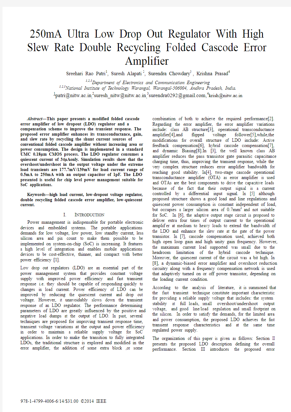
The LDO regulator constitutes error am transistor (Mpass), and feedback resistorsRf1Fig.1.
The error amplifier generates error signal th
transistor to regulate the output. Power tra large parasitic capacitance at its input due to drives large load current. The load current output leads to the spikes generations and r being: speed of the load variations, present at the output of LDO, loop ban phase margin. But, the dominating factor a slew rate at the gate of the pass transistor [3, 5
Fig.1. Proposed Low drop ou The voltage droop derived from capacitor c given as,
10
load
t I V t C Δ=
Δ Where
t V Δ is the transient voltage droop,current step,0C is the output load capacitanc taken by the loop to respond.
11
SR t t BW
Δ=
+ BW is the closed loop bandwidth of LDO, S t loop delay caused due to slew rate at the transistor. The drop in the transient response change is to be reduced as it has detrimental devices. So, the bandwidth of error amplifi and large slew rate for faster transient respon between slew rate and high power consum considered as well.
III. P ROPOSED E RROR A MPL
The conventional PMOS Folded Cascode unique benefits of lower flicker noise,
high sation and circuit ts the simulation .
PTION mplifier, a power
1, Rf2 as shown in hat drives the pass ansistor exhibits a its large area for it t variations at the responsible factors load capacitance ndwidth, and loop among them is the 5-7].
ut Regulator
current equation is
(1)
, load I is the load
ce, 1t Δ is the time
(2)
SR is the additional e gate of the pass e for a load current l effect on the load ier has to be large se, but the tradeoff mption has to be LIFIER e Amplifier with its
her non dominant
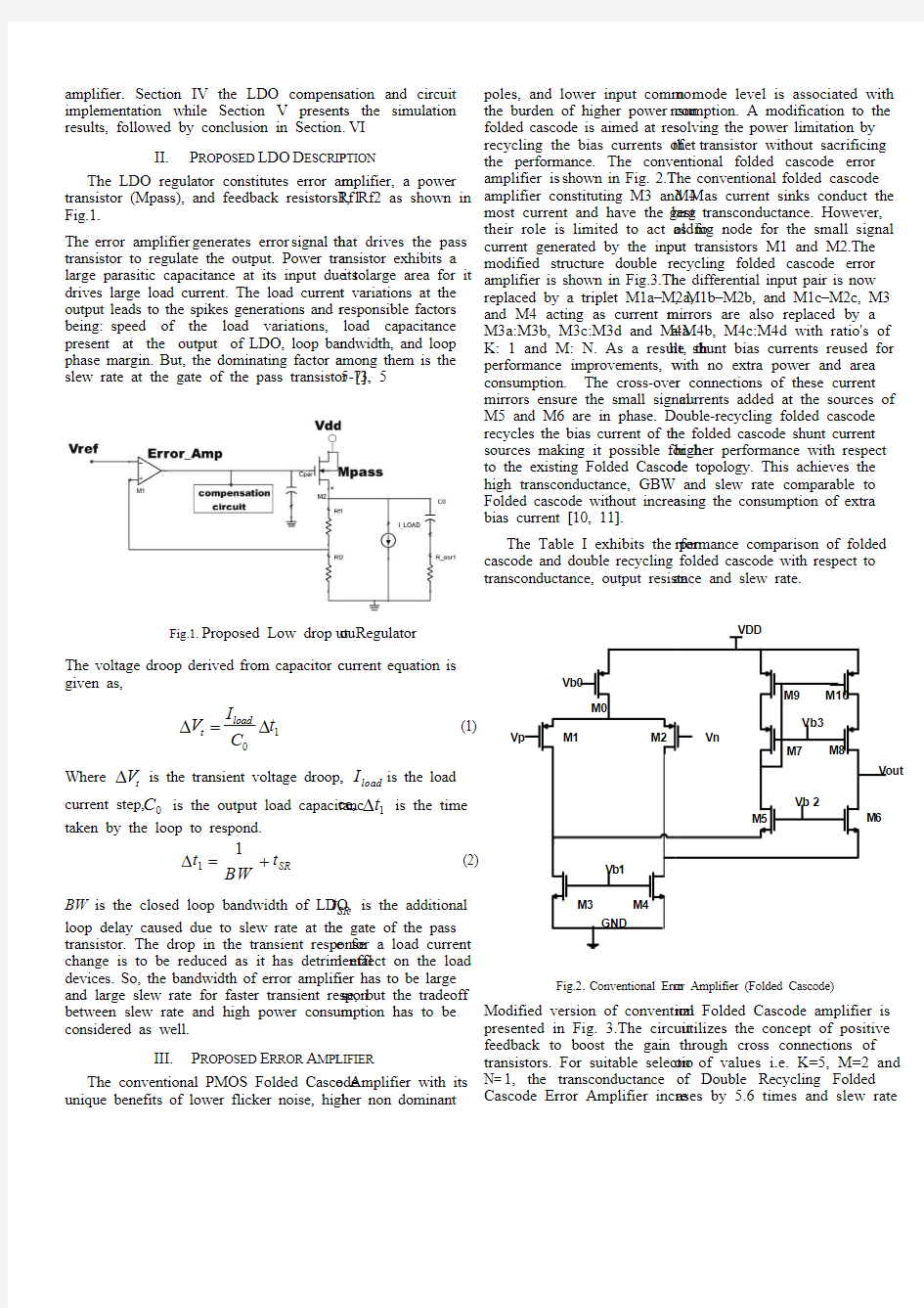
poles, and lower input commo the burden of higher power con folded cascode is aimed at res recycling the bias currents of t the performance. The conve amplifier is shown in Fig. 2.T amplifier constituting M3 and M most current and have the larg their role is limited to act as fo current generated by the inpu modified structure double re amplifier is shown in Fig.3.Th replaced by a triplet M1a–M2a,and M4 acting as current m M3a:M3b, M3c:M3d and M4a K: 1 and M: N. As a result, th performance improvements, w consumption. The cross-over mirrors ensure the small signal M5 and M6 are in phase. D recycles the bias current of th sources making it possible for h to the existing Folded Cascod high transconductance, GBW Folded cascode without increa bias current [10, 11].
The Table I exhibits the per
cascode and double recycling transconductance, output resista
Fig.2. Conventional Erro Modified version of convention presented in Fig. 3.The circuit feedback to boost the gain transistors. For suitable selectio N=1, the transconductance Cascode Error Amplifier incre n mode level is associated with
nsumption. A modification to the solving the power limitation by the transistor without sacrificing entional folded cascode error The conventional folded cascode M4 as current sinks conduct the gest transconductance. However, olding node for the small signal ut transistors M1 and M2.The ecycling folded cascode error he differential input pair is now , M1b–M2b, and M1c–M2c, M3 mirrors are also replaced by a a:M4b, M4c:M4d with ratio's of he shunt bias currents reused for with no extra power and area r connections of these current currents added at the sources of ouble-recycling folded cascode he folded cascode shunt current higher performance with respect de topology. This achieves the and slew rate comparable to asing the consumption of extra rformance comparison of folded folded cascode with respect to ance and slew rate.
or Amplifier (Folded Cascode)
nal Folded Cascode amplifier is
utilizes the concept of positive through cross connections of on of values i.e. K=5, M=2 and of Double Recycling Folded ases by 5.6 times and slew rate
by 3.75 times comparable to that of Folded Cascode Amplifier. The increased slew rate of error amplifier improves the transient response. The speed of LDO improves for the increase in the GBW [11].
IV.LDO COMPENSATION
The compensation of LDO for the low values of load capacitance of 1pF (capacitor less) is much critical. The basic miller capacitance used as that of conventional low drop regulator falls short of meeting the criteria of generating regulated output voltage for SoC as its value needs to be large and thus integration problems. An additional fast loop (differentiator) is employed as compensation circuit which solves the dual purpose of output transient detection to improve the transient response and internal ac compensation is shown in Fig .4.
TABLE I . COMPARISON OF THE PROPOSED CAPACITOR-LESS LDO
TOPOLOGY AGAINST THE STATE OF ART [11]
The compensation circuitry is composed of differentiator (C 1, R 1, and gm 21) and an additional transistor M 20 to boost the feedback gain and increase in effective capacitance value for compensation. For the change in the load current, induces a corresponding change in the output voltage which in turn generates a current through the
capacitor C 1.The current is then injected to pass transistor gate capacitance improves speed of charging thus assisting in regulating output voltage. The current through C 1 being bidirectional responds to both positive and negative deflections at the output [12].
Fig.3. Proposed error amplifier (Double Recycling folded cascode)
Fig.4. LDO Schematic
IV. SIMULATION RESULTS
The proposed LDO regulator is simulated in the UMC 180nm CMOS process using cadence tool.
A. Transient Response
Fig.5 and Fig.6 demonstrates the circuit transient response under load current changes from 0.5mA to 250mA for 1μs. The voltage undershoot is about 139mV. The output voltage returns to its regulated value within settling time of 1.147μs. The load transient response conf rms that the proposed regulator is stable for whole range of load currents.
Fig.5. Simulated Transient Response of LDO
Fig.6. Transient response for Load current (0.5 to 200mA).
Fig.7. Loop gain and phase response for different load current
B. Loop gain and phase response
Fig. 7 shows the frequency response of proposed LDO regulator at 0.5mA and 250mA of load current. It is shown that the unity gain frequency of the proposed LDO regulator is 2.432MHz and3.73MHz for 0.5mAand 200mA respectively. While the phase margin is 70.10and 680 correspondingly. So, the proposed LDO regulator is stable for large load current changes.
Table-II reports the simulation results comparison between proposed LDOs and recent works. The figure of merit FOM= (T R xI Q )/I MAX = ((C OUT x ?V OUT )/I MAX ) x (I Q /I MAX ) from Ref [22] is adapted here to compare the transient response of different LDOs in which ?V OUT is the maximum output voltage variation due to the load transient. Lower FOM signifies better transient response achieved by the LDO. The use of double recycling folded cascode error amplifier with high slew rate and low quiescent current resulted in better FOM of value 0.0778μs.
T ABLE II . C OMPARISON OF THE PROPOSED CAPACITOR -LESS LDO TOPOLOGY AGAINST THE STATE OF THE ART
[12] [13]
[16] [2] [14] [17] [18] [19] [20] [21] [3] [15] This
work
Year 2007 2007 2007 2010 2010 2010 2012 2012 2012 2012 2013 2014 2014 Tech.[μm] 0.35 0.35 0.18 0.35 0.35 0.35 0.13 0.18 0.35 0.065 0.11 0.18 0.18 V Drop [mV] 200 200 200 200 200 200 200 N-A 150 200 200 200 200 C OUT 0-100pf 1μf 100pf 100pf 0.5μf 100pf 20pf 100pf 100pf 100pf 40pf 100pf 1pf I Max [mA] 50 200 50 100 200 100 50 5 100 100 0.5-200 100 0.5-250 I Q [mA] 0.065 0.02 0.0012 0.02 0.06 0.02 0.037 0.12 0.007 0.0824 0.0415 0.0037 0.034 ?V OUT [mV] 90 54 490 97 60 100 56 170 236 68.8 385 277 139 Settling Time Ts[μs] 15 N.A 4.4 9 8 8 0.4 1.4 0.15 6 0.61 6 1.147 Current
efficiency[%] 99.87 99.99 99.99 99.98 99.97 99.98 99.92 97.65 99.99 99.91 99.98 99.99 99.98 FOM[ns]
234
270
23.5μ
19.4 μ
450
20μ
19.4μ
81.6μ
16.52μ
56.69μ
15.97μ
10.2μ
0.0778μ
VI.C ONCLUSION
This paper presented a stable LDO voltage regulator with a novel Double Recycling Folded Cascode Error Amplifier structure. It influenced the GBW and slew rate for improving the transient response and settling time.LDO is validated through simulation results exhibiting the output voltage spike of a value 177.7mV, when the output current changes from 250 to 0.5mA,139mV for the current change from 0.5 to 200mA and settling time was 1.147μs .The stability of system is ensured for different load currents of 0.5mA and 200mA.The use of low value of compensation capacitors (C1=500fF)saves chip-area and multiple proposed LDO regulators can be applied in chip-level power management.
This scheme solves the problems of limited bandwidth and slew rate in the conventional LDO by applying a simple and effective modification to the conventional LDO circuit using improved folded cascode error amplifier.
R EFERENCES
[1]H. Eul. ICs for mobile multimedia communications.. in Proc.
IEEE ISSCC Dig. Tech. Papers. Feb. 2006, pp. 21-39.
[2] E. N. Y. Ho and P. K. T. Mok, “A capacitor-less CMOS active
feedback low-dropout regulator with slew-rate enhancement for portable on-chip application,”IEEE Trans. Circuits Syst. II, Exp.
Briefs, vol. 57, no. 2,pp. 80–84, Feb. 2010.
[3]Young-Il Kim; Sang-sun Lee, "A Capacitor less LDO Regulator
With Fast Feedback Technique and Low-Quiescent Current Error Amplifier," Circuits and Systems II: Express Briefs, IEEE Transactions on , vol.60, no.6, pp.326,330, June 2013.
[4]Martinez-Garcia, H.; Grau-Saldes, A.; Bolea-Monte, Y.,
"Design of a 4.5-V, 450-mA low-dropout voltage linear regulator based on a cascoded OTA," Industrial Electronics Society, IECON 2013 - 39th annual Conference of the IEEE , vol., no., pp.2244,2249, 10-13 Nov. 2013.
[5]Hinojo, J. M., et al. "Internally compensated LDO regulator
based on the cascoded FVF." Microelectronics Journal (2014).
[6]Qu, Xi, Ze-kun Zhou, and Bo Zhang. "A fully on-chip 1-μW
capacitor-free low-dropout regulator with adaptive output stage." Analog Integrated Circuits and Signal Processing 78.2 (2014): 353-360.
[7]Aminzadeh, H.; Serdijn, W., "Low-dropout regulators: Hybrid-
cascode compensation to improve stability in nano-scale CMOS technologies," Circuits and Systems (ISCAS), 2011 IEEE International Symposium on , vol., no., pp.2293,2296, 15-18 May 2011.
[8]Chong, SauSiong, and Pak Kwong Chan. "A 0.9-/spl mu/A
Quiescent Current Output-Capacitor less LDO Regulator With Adaptive Power Transistors in 65-nm CMOS." Circuits and Systems I: Regular Papers, IEEE Transactions on 60.4 (2013): 1072-1081. [9]P. Y. Or and K. N. Leung, “An output-capacitorless low-dropout
regulator with direct voltage-spike detection,”IEEE J. Solid-State Circuits, vol. 45,no. 2, pp. 458–466, Feb. 2010.
[10]Assaad, R., & Silva-Martinez, J. (2009). ‘The recycling folded
cascode: A general enhancement of the folded cascade amplifier’.IEEE Journal of Solid-State Circuits, 44(9), 2535–2542.
[11]Yan, Z., Mak, P.-I., and Martins, R.P. (2012), ‘Double
Recycling Technique for Folded-cascode OTA’,Analog Integrated Circuits and Signal Processing, 71, 137–141. [12]R. J. Milliken , J. Silva-Martinez and E. Sanchez-Sinencio "Full
on-chip CMOS low-dropout voltage regulator", IEEE Trans.
Circuits Syst. I, Reg. Papers, vol. 54, no. 9, pp.1879 -1890 2007
[13]Al-Shyoukh, Mohammad, Hoi Lee, and Raul Perez. "A
transient-enhanced low-quiescent current low-dropout regulator with buffer impedance attenuation."Solid-State Circuits, IEEE Journal of 42.8 (2007): 1732-1742.
[14]Yeong-Tsair Lin; Chi-Cheng Wu; Mei-Chu Jen; Dong-Shiuh
Wu; Zhe-Wei Wu, "A Low Dropout regulator using current buffer compensation technique," Solid-State and Integrated Circuit Technology (ICSICT), 2010 10th IEEE International Conference on , vol., no., pp.144,146, 1-4 Nov. 2010
[15]Fathipour, Rasoul, et al. "High slew rate current mode
transconductance error amplifier for low quiescent current output-capacitorless CMOS LDO regulator."Integration, the VLSI Journal 47.2 (2014): 204-212.
[16]T.Y. Man, P.K.T. Mok, M. Chan A high slew-rate push-pull
output amplifier for low-quiescent current low-dropout regulators with transient-response improvement IEEE Trans.
Circuits Syst. Express Briefs, 54 (9) (2007), pp. 755–759. [17]E.N.Y. Ho, P.K.T. Mok, A capacitor-less CMOS active
feedback low-dropout regulator with slew-rate enhancement for portable on-chip applications, IEEETrans. Circuits Syst. Express Briefs 57 (2) (2010) 80–84.
[18]E. N. Y. Ho and P. K. T. Mok, “Wide-loading-range fully
integrated LDR with a power-supply ripple injection filter,”IEEE Trans. Circuits Syst. II,Exp. Briefs, vol. 59, no. 6, pp. 356–360, Jun. 2012.
[19]J. H. Wang, C. H. Tsai, and S. W. Lai, “A low-dropout regulator
with tail current control for DPWM clock correction,”IEEE Trans. Circuits Syst.II, Exp. Briefs, vol. 59, no. 1, pp. 45–49, Jan. 2012.
[20]X. Ming, Q. Li, Z. Zhou, and B. Zhang, “An ultrafast adaptively
biased capacitorless LDO with dynamic charging control,”IEEE Trans. Circuits Syst. II, Exp. Briefs, vol. 59, no. 1, pp. 40–44, Jan. 2012.
[21]S. S. Chong and P. K. Chan, “A 0.9-A quiescent current output
capacitorless LDO regulator with adaptive power transistors in 65-nm CMOS,”IEEE Trans. Circuits Syst. I, Reg. Papers, vol.
60, no. 4,pp. 1072–1081, Apr. 2013.
[22]P. Hazucha and B. A. Bloechel, “Area-efficient linear regulator
with ultrafast load regulation,”IEEE J. Solid-State Circuits, vol.
40, no. 4, pp. 933–940, Apr. 2005.