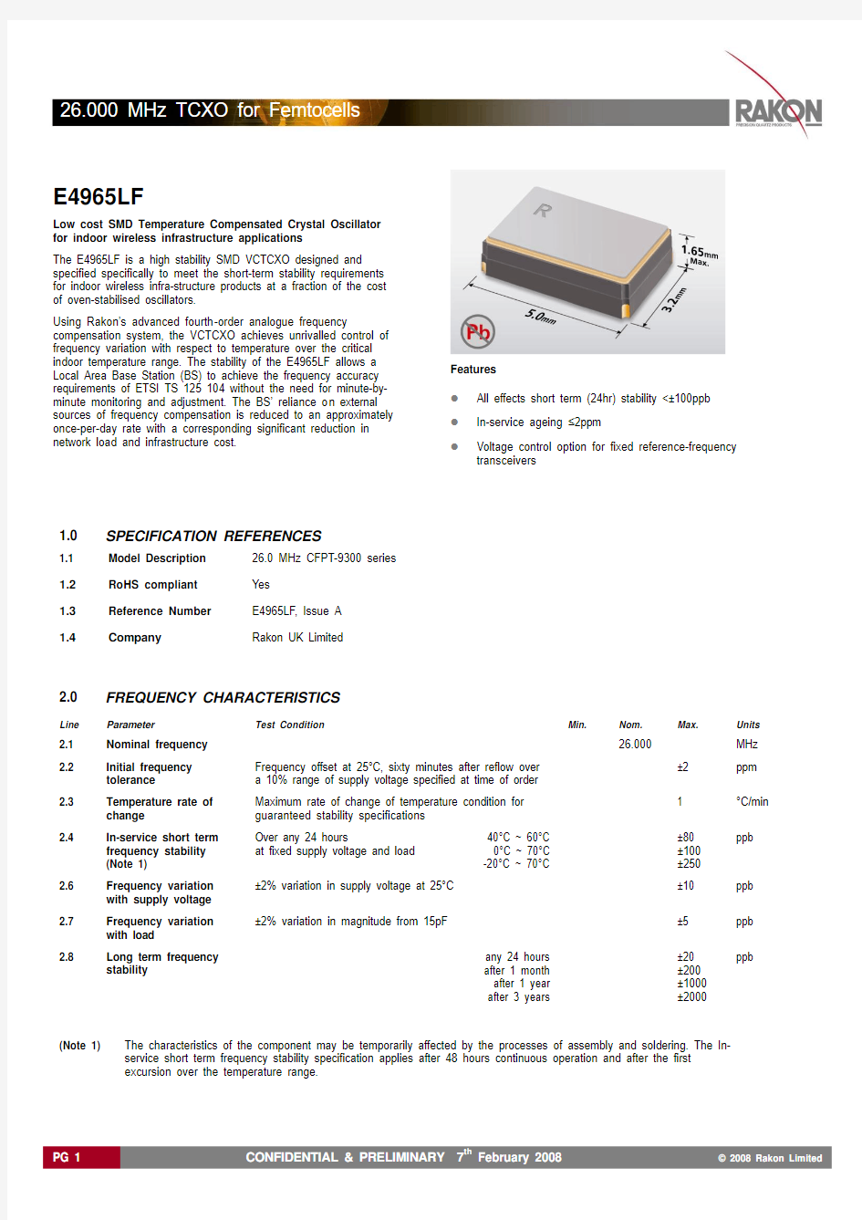
E4965LF
Low cost SMD Temperature Compensated Crystal Oscillator for indoor wireless infrastructure applications
The E4965LF is a high stability SMD VCTCXO designed and specified specifically to meet the short-term stability requirements for indoor wireless infra-structure products at a fraction of the cost of oven-stabilised oscillators.
Using Rakon’s advanced fourth -order analogue frequency
compensation system, the VCTCXO achieves unrivalled control of frequency variation with respect to temperature over the critical indoor temperature range. The stability of the E4965LF allows a Local Area Base Station (BS) to achieve the frequency accuracy requirements of ETSI TS 125 104 without the need for minute-by-minute monitoring and adjustment. The BS’ reliance o n external sources of frequency compensation is reduced to an approximately once-per-day rate with a corresponding significant reduction in network load and infrastructure cost.
Features
? All effects short term (24hr) stability <±100ppb ? In-service ageing ≤2ppm
?
Voltage control option for fixed reference-frequency transceivers
1.0
SPECIFICATION REFERENCES
1.1 Model Description 26.0 MHz CFPT-9300 series 1.2 RoHS compliant Yes
1.3 Reference Number E4965LF, Issue A 1.4 Company
Rakon UK Limited
2.0
FREQUENCY CHARACTERISTICS
Line
Parameter
Test Condition
Min.
Nom.
Max.
Units
2.1 Nominal frequency
26.000 MHz 2.2 Initial frequency tolerance
Frequency offset at 25°C, sixty minutes after reflow over a 10% range of supply voltage specified at time of order ±2 ppm 2.3 Temperature rate of change
Maximum rate of change of temperature condition for guaranteed stability specifications 1 °C/min 2.4
In-service short term frequency stability (Note 1)
Over any 24 hours
40°C ~ 60°C at fixed supply voltage and load 0°C ~ 70°C
-20°C ~ 70°C
±80 ±100 ±250 ppb
2.6 Frequency variation with supply voltage ±2% variation in supply voltage at 25°C ±10 ppb 2.7 Frequency variation with load
±2% variation in magnitude from 15pF ±5 ppb 2.8
Long term frequency stability
any 24 hours after 1 month after 1 year
after 3 years
±20 ±200 ±1000 ±2000
ppb
(Note 1)
The characteristics of the component may be temporarily affected by the processes of assembly and soldering. The In-service short term frequency stability specification applies after 48 hours continuous operation and after the first excursion over the temperature range.
3.0 POWER SUPPLY
Line Parameter Test Condition Min. Max. Units
3.1 Supply voltage 3.14 3.46 V
3.2 Supply current 3.3V, load 10k?//10pF 3.0 mA
4.0 OSCILLATOR OUTPUT
Line Parameter Description/Test Condition Min. Max. Units
4.1 Output waveform DC coupled Clipped Sinewave
4.2 Output voltage level 0.8 Vpp
4.3 Output load resistance 10k ?
4.4 Output load
10 pF
capacitance
5.0 SSB PHASE NOISE
Line Parameter Test Condition Min. Max. Units
5.1 SSB PSD At 1Hz frequency offset from carrier -58 dBc/Hz
5.2 SSB PSD At 10Hz frequency offset from carrier -87 dBc/Hz
5.3 SSB PSD At 100Hz frequency offset from carrier -109 dBc/Hz
5.4 SSB PSD At 1kHz frequency offset from carrier -122 dBc/Hz
5.5 SSB PSD At 10kHz frequency offset from carrier -132 dBc/Hz
6.0 JITTER
Line Parameter Test Condition Min. Max. Units
6.1 Jitter Frequency offset from carrier 10Hz to 1MHz 1.7 psec
7.0 VOLTAGE CONTROL
Line Parameter Test Condition Min. Max. Units
7.1 Tuning range ±5 ±10 ppm
7.2 Control voltage Vcc = 3.3V 0.5 2.5 V
7.3 Input resistance 100k Ω
8.0 ENVIRONMENTAL
Line Parameter Test Condition Min. Max. Units
8.1 Storage temperature -40 85 °C
8.2 Shock IEC 60068-2-27, test Ea: 1500gn acceleration for 0.5ms duration, Half-sine pulse, three shocks in
each direction along three mutually perpendicular axes.
8.3 Humidity 85% for 48 hours at 85°C, non-condensing
Outline:
Pin Function
1 Control Voltage, Vc
2 Ground
3 Output
4 Supply Voltage, Vs
Note: for correct operation a 10nF supply de-
coupling capacitor should be placed next to the
device, see recommended PCB pattern. If an AC
coupled output is required a 10nF should be
placed in series with output pad 3.
Marking:
Manufacturers ID (R)
Manufacturing identifier (X XX)
Pad 1 / Static Sensitivity Identifier ( )
Abbreviated Part Number (4965)
Device date code (YW)
Notes: 1) Sample marking may vary.
2) Parts may be marked 'CMAC' (a trademark used under licence) instead of 'R' for a limited time.
Rakon Limited (Rest of world) One Pacific Rise, Mt Wellington Auckland 1006, New Zealand Phone: +64 (9) 573 5554 Fax: +64 (9) 573 5559 Email: sales@https://www.doczj.com/doc/643283902.html,
Rakon America (North, Central America) Chicago, IL, USA
Email: sales@https://www.doczj.com/doc/643283902.html, Rakon Europe (Europe, Middle East, Africa) Crewkerne, Somerset, UK
Email: info@https://www.doczj.com/doc/643283902.html,
Rakon Asia (China, Taiwan, Korea, SE Asia)
Taipei, Taiwan, ROC
Email: sales@https://www.doczj.com/doc/643283902.html,
Email: sales@https://www.doczj.com/doc/643283902.html,
Copyright ? Rakon Limited 2008