General Description
The MAX1036–MAX1039 low-power, 8-bit, multichannel,analog-to-digital converters (ADCs) feature internal track/hold (T/H), voltage reference, clock, and an I 2C-compatible 2-wire serial interface. These devices operate from a single supply and require only 350μA at the maximum sampling rate of 188ksps. Auto-Shutdown? powers down the devices between conver-sions reducing supply current to less than 1μA at low throughput rates. The MAX1036/MAX1037 have four ana-log input channels each, while the MAX1038/MAX1039have twelve analog input channels. The analog inputs are software configurable for unipolar or bipolar and single-ended or pseudo-differential operation.
The full-scale analog input range is determined by the internal reference or by an externally applied reference voltage ranging from 1V to V DD . The MAX1037/MAX1039 feature a 2.048V internal reference and the MAX1036/MAX1038 feature a 4.096V internal reference.The MAX1036/MAX1037 are available in 8-pin SOT23packages. The MAX1038/MAX1039 are available in 16-pin QSOP packages. The MAX1036–MAX1039 are guar-anteed over the extended industrial temperature range (-40°C to +85°C). Refer to MAX1136–MAX1139 for 10-bit devices and to the MAX1236–MAX1239 for 12-bit devices.
Applications
Hand-Held Portable Applications Medical Instruments
Battery-Powered Test Equipment Solar-Powered Remote Systems Received-Signal-Strength Indicators System Supervision
Features
o High-Speed I 2C-Compatible Serial Interface
400kHz Fast Mode
1.7MHz High-Speed Mode o Single Supply
2.7V to
3.6V (MAX1037/MAX1039)
4.5V to
5.5V (MAX1036/MAX1038)o Internal Reference
2.048V (MAX1037/MAX1039)4.096V (MAX1036/MAX1038)o External Reference: 1V to V DD o Internal Clock
o 4-Channel Single-Ended or 2-Channel Pseudo-Differential (MAX1036/MAX1037)o 12-Channel Single-Ended or 6-Channel Pseudo-Differential (MAX1038/MAX1039)o Internal FIFO with Channel-Scan Mode o Low Power
350μA at 188ksps 110μA at 75ksps 8μA at 10ksps
1μA in Power-Down Mode
o Software Configurable Unipolar/Bipolar o Small Packages
8-Pin SOT23 (MAX1036/MAX1037)16-Pin QSOP (MAX1038/MAX1039)
MAX1036–MAX1039
2.7V to 5.5V , Low-Power, 4-/12-Channel
2-Wire Serial 8-Bit ADCs
________________________________________________________________Maxim Integrated Products 1
Ordering Information
19-2442; Rev 1; 10/02
For pricing, delivery, and ordering information,please contact Maxim/Dallas Direct!at 1-888-629-4642, or visit Maxim’s website at https://www.doczj.com/doc/612686727.html,.
AutoShutdown is a trademark of Maxim Integrated Products, Inc.
Pin Configura tions a nd Typica l Opera ting Circuit a ppea r at end of data sheet.
M A X 1036–M A X 1039
2.7V to 5.5V , Low-Power, 4-/12-Channel 2-Wire Serial 8-Bit ADCs
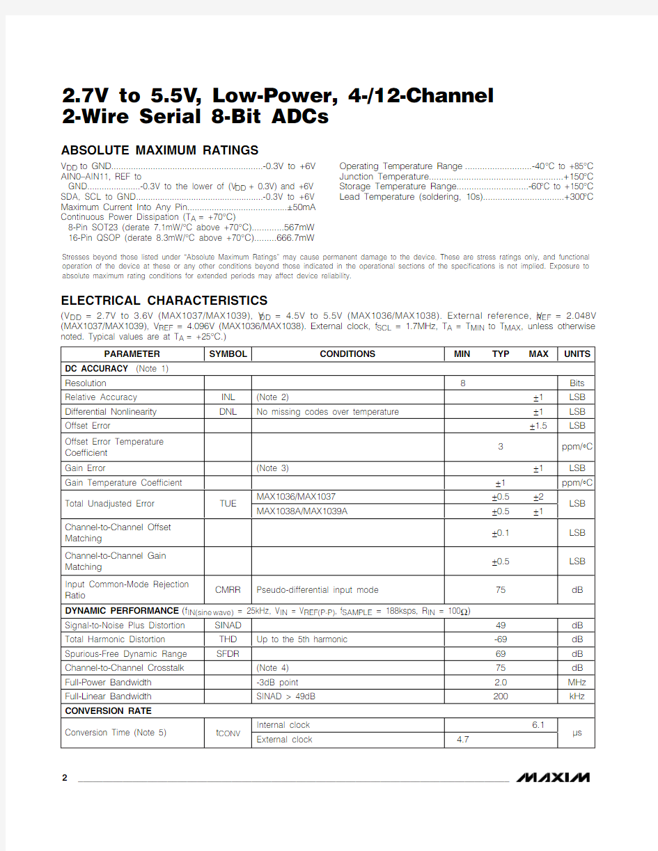
ABSOLUTE MAXIMUM RATINGS
ELECTRICAL CHARACTERISTICS
(V DD = 2.7V to 3.6V (MAX1037/MAX1039), V DD = 4.5V to 5.5V (MAX1036/MAX1038). External reference, V REF = 2.048V (MAX1037/MAX1039), V REF = 4.096V (MAX1036/MAX1038). External clock, f SCL = 1.7MHz, T A = T MIN to T MAX , unless otherwise noted. Typical values are at T A = +25°C.)
Stresses beyond those listed under “Absolute Maximum Ratings” may cause permanent damage to the device. These are stress ratings only, and functional operation of the device at these or any other conditions beyond those indicated in the operational sections of the specifications is not implied. Exposure to absolute maximum rating conditions for extended periods may affect device reliability.
V DD to GND..............................................................-0.3V to +6V AIN0–AIN11, REF to
GND......................-0.3V to the lower of (V DD + 0.3V) and +6V SDA, SCL to GND.....................................................-0.3V to +6V Maximum Current Into Any Pin.........................................±50mA Continuous Power Dissipation (T A = +70°C)
8-Pin SOT23 (derate 7.1mW/°C above +70°C).............567mW 16-Pin QSOP (derate 8.3mW/°C above +70°C).........666.7mW
Operating Temperature Range ...........................-40°C to +85°C Junction Temperature......................................................+150°C Storage Temperature Range.............................-60°C to +150°C Lead Temperature (soldering, 10s).................................+300°C
MAX1036–MAX1039
2.7V to 5.5V , Low-Power, 4-/12-Channel
2-Wire Serial 8-Bit ADCs
_______________________________________________________________________________________3
ELECTRICAL CHARACTERISTICS (continued)
(V DD = 2.7V to 3.6V (MAX1037/MAX1039), V DD = 4.5V to 5.5V (MAX1036/MAX1038). External reference, V REF = 2.048V (MAX1037/MAX1039), V REF = 4.096V (MAX1036/MAX1038). External clock, f SCL = 1.7MHz, T A = T MIN to T MAX , unless otherwise noted. Typical values are at T A = +25°C.)
M A X 1036–M A X 1039
2.7V to 5.5V , Low-Power, 4-/12-Channel 2-Wire Serial 8-Bit ADCs 4_______________________________________________________________________________________
ELECTRICAL CHARACTERISTICS (continued)
(V DD = 2.7V to 3.6V (MAX1037/MAX1039), V DD = 4.5V to 5.5V (MAX1036/MAX1038). External reference, V REF = 2.048V (MAX1037/MAX1039), V REF = 4.096V (MAX1036/MAX1038). External clock, f SCL = 1.7MHz, T A = T MIN to T MAX , unless otherwise noted. Typical values are at T A = +25°C.)
MAX1036–MAX1039
2.7V to 5.5V , Low-Power, 4-/12-Channel
2-Wire Serial 8-Bit ADCs
_______________________________________________________________________________________
5
ELECTRICAL CHARACTERISTICS (continued)
(V DD = 2.7V to 3.6V (MAX1037/MAX1039), V DD = 4.5V to 5.5V (MAX1036/MAX1038). External reference, V REF = 2.048V (MAX1037/MAX1039), V REF = 4.096V (MAX1036/MAX1038). External clock, f SCL = 1.7MHz, T A = T MIN to T MAX , unless otherwise noted. Typical values are at T
= +25°C.)
ured for unipolar, single-ended inputs.
Note 2:Relative accuracy is the deviation of the analog value at any code from its theoretical value after the full-scale range and
offsets have been calibrated.
Note 3:Offset nulled.
Note 4:Ground ON channel; sine wave applied to all OFF channels.
Note 5:Conversion time is defined as the number of clock cycles (8) multiplied by the clock period. Conversion time does not
include acquisition time. SCL is the conversion clock in the external clock mode.
Note 6:The absolute voltage range for the analog inputs (AIN0–AIN11) is from GND to V DD .
Note 7:When AIN_/REF is configured to be an internal reference (SEL[2:1] = 11), decouple AIN_/REF to GND with a 0.01μF capacitor.Note 8:The switch connecting the reference buffer to AIN_/REF has a typical on-resistance of 675?.Note 9:ADC performance is limited by the converter ’s noise floor, typically 1.4mV P-P .
Note 10:Electrical characteristics are guaranteed from V DD(min)to V DD(max). For operation beyond this range, see the Typical
Operating Characteristics .
Note 11:Power-supply rejection ratio is measured as:
REF = 2.048V.
Power-supply rejection ratio is measured as:
REF = 2.048V.
Note 12:A master device must provide a data hold time for SDA (referred to V IL of SCL) in order to bridge the undefined region of
SCL ’s falling edge (Figure 1).
Note 13:C B = total capacitance of one bus line in pF. t R and t F measured between 0.3V DD and 0.7V DD . Minimum specification is
tested at +25°C with C B = 400pF.
Note 14:f SCLH must meet the minimum clock low time plus the rise/fall times.
M A X 1036–M A X 1039
2.7V to 5.5V , Low-Power, 4-/12-Channel 2-Wire Serial 8-Bit ADCs 6_______________________________________________________________________________________
Typical Operating Characteristics
(V DD = 3.3V (MAX1037/MAX1039), V DD = 5V (MAX1036/MAX1038), f SCL = 1.7MHz, external clock (33% duty cycle), f SAMPLE = 188ksps,single ended, unipolar, T A = +25°C, unless otherwise noted.)
150
250200350300400450SUPPLY CURRENT vs. VOLTAGE
V DD (V)
I D D (μA )
2.5
3.5
4.03.0
4.5
5.0 5.5
150
250200350300400
450-40
85
SUPPLY CURRENT vs. TEMPERATURE
TEMPERATURE (°C)
I D D (μA )
10
-15
35
60
1
3
2
4
5
2.5
3.5
3.0
4.0 4.5
5.0
5.5
SHUTDOWN SUPPLY CURRENT
vs. SUPPLY VOLTAGE
V DD (V)
I D D (
μA )
01
3
2
4
5
-40
10
-15
35
60
85
SHUTDOWN SUPPLY CURRENT
vs. TEMPERATURE
TEMPERATURE (°C)
I D D (μA )
10050
2001503002503500
20
30
10
40
50
60
AVERAGE SUPPLY CURRENT vs. CONVERSION RATE (INTERNAL CLOCK)
CONVERSION RATE (ksps)
A V E R A G E I D D (μA )
150100
50300250200450400350500
100
50
150
200
AVERAGE SUPPLY CURRENT VS. CONVERSION RATE (EXTERNAL CLOCK)
CONVERSION RATE (ksps)
A V E R A G E I D D (μA )
0.9900
0.99250.99500.99751.00001.00251.00501.00751.01004.00
4.50
4.25
4.75
5.00
5.25
5.50
NORMALIZED 4.096V REFERENCE VOLTAGE
vs. SUPPLY VOLTAGE
M A X 1036 t o c 7
V DD (V)
V R E F N O R M A L I Z E D
0.980
0.9850.9900.9951.0001.0051.0101.0151.020-40
-15
10
35
60
85INTERNAL 4.096V REFERENCE VOLTAGE
vs. TEMPERATURE
M A X 1036 t o c 08
TEMPERATURE (°C)
V R E F N O R M A L I Z E D
0.9900
0.99250.99500.99751.00001.00251.00501.00751.0100
2.5
3.53.0
4.0 4.5
5.0 5.5
INTERNAL 2.048V REFERENCE VOLTAGE
vs. SUPPLY VOLTAGE
M A X 1036 t o c 09
V DD (V)
V R E F N O R M A L I Z E D
MAX1036–MAX1039
2.7V to 5.5V , Low-Power, 4-/12-Channel
2-Wire Serial 8-Bit ADCs
_______________________________________________________________________________________7
0.980
0.9850.9900.9951.0001.0051.0101.0151.020-40
-15
10
35
60
85
INTERNAL 2.048V REFERENCE VOLTAGE
vs. TEMPERATURE
M A X 1036 t o c 10
TEMPERATURE (°C)
V R E F N O R M A L I Z E D
-0.5
-0.2-0.3-0.4-0.100.10.20.30.40.5010050150200250300DIFFERENTIAL NONLINEARITY
vs. DIGITAL CODE
M A X 1036 t o c 11
DIGITAL OUTPUT CODE D N L (L S B )
-0.5
-0.2-0.3-0.4-0.100.10.20.30.40.5
010050150200250300
INTEGRAL NONLINEARITY
vs. DIGITAL CODE
M A X 1036 t o c 12
DIGITAL OUTPUT CODE
I N L (L S B )
-120
-80-100-40-60-2000
100k
FFT PLOT
FREQUENCY (Hz)
A M P L I T U D E (d
B c )
40k
20k
60k
80k
0.30.20.1
0.40.50.60.70.80.91.0
2.5
3.5
3.0
4.0 4.5
5.0
5.5
OFFSET ERROR vs. SUPPLY VOLTAGE
V DD (V)
O F F S E T E R R O R (L S B )
0.30.20.10.40.50.60.70.80.91.0-4010-15356085OFFSET ERROR vs. TEMPERATURE
TEMPERATURE (°C)
O F F S E T E R R O R (L S B )
-0.1
-0.07-0.08-0.09-0.06-0.05-0.04-0.03-0.02-0.010
2.5
3.53.0
4.0 4.5
5.0 5.5
GAIN ERROR vs. SUPPLY VOLTAGE
V DD (V)
G A I N E R R O R (L S B )Typical Operating Characteristics (continued)
(V DD = 3.3V (MAX1037/MAX1039), V DD = 5V (MAX1036/MAX1038), f SCL = 1.7MHz, external clock (33% duty cycle), f SAMPLE = 188ksps,single ended, unipolar, T A = +25°C, unless otherwise noted.)
M A X 1036–M A X 1039
Detailed Description
The MAX1036–MAX1039 ADCs use successive-approximation conversion techniques and input T/H cir-cuitry to capture and convert an analog signal to a serial 8-bit digital output. The MAX1036/MAX1037 are 4-channel ADCs, and the MAX1038/MAX1039 are 12-channel ADCs. These devices feature a high-speed 2-wire serial interface supporting data rates up to 1.7MHz. Figure 3 shows the simplified functional dia-gram for the MAX1038/MAX1039.
Power Supply
The MAX1036–MAX1039 operate from a single supply and consume 350μA at sampling rates up to 188ksps.The MAX1037/MAX1039 feature a 2.048V internal reference and the MAX1036/MAX1038 feature a 4.096V internal reference. All devices can be configured for use with an external reference from 1V to V DD .
Analog Input and Track/Hold
The MAX1036–MAX1039 analog input architecture con-tains an analog input multiplexer (MUX), a T/H capaci-tor, T/H switches, a comparator, and a switched capacitor digital-to-analog converter (DAC) (Figure 4).In single-ended mode, the analog input multiplexer con-nects C T/H to the analog input selected by CS[3:0] (see the Configuration/Setup Bytes (Write Cycle) section). The charge on C T/H is referenced to GND when converted. In pseudo-differential mode, the analog input multiplexer connects C T/H to the ‘+’analog input selected by CS[3:0]. The charge on C T/H is referenced to the ‘-’ ana-log input when converted.
The MAX1036–MAX1039 input configuration is pseudo-differential in that only the signal at the ‘+’ analog input is sampled with the T/H circuitry. The ‘-’ analog input signal must remain stable within ±0.5LSB (±0.1LSB for best results) with respect to GND during a conversion.To accomplish this, connect a 0.1μF capacitor from ‘-’analog input to G ND. See the Single-Ended/Pseudo-Differential Input section.
During the acquisition interval, the T/H switches are in the track position and C T/H charges to the analog input signal. At the end of the acquisition interval, the T/H switches move to the hold position retaining the charge on C T/H as a sample of the input signal.
During the conversion interval, the switched capacitive DAC adjusts to restore the comparator input voltage to zero within the limits of 8-bit resolution. This action requires eight conversion clock cycles and is equiva-lent to transferring a charge of 18pF ?(V IN + - V IN -)from C T/H to the binary weighted capacitive DAC form-ing a digital representation of the analog input signal.Sufficiently low source impedance is required to ensure an accurate sample. A source impedance below 1.5k ?does not significantly degrade sampling accuracy. To minimize sampling errors with higher source imped-ances, connect a 100pF capacitor from the analog input to G ND. This input capacitor forms an RC filter with the source impedance limiting the analog input bandwidth. For larger source impedances, use a buffer amplifier to maintain analog input signal integrity.
When operating in internal clock mode, the T/H circuitry enters its tracking mode on the ninth falling clock edge
2.7V to 5.5V , Low-Power, 4-/12-Channel 2-Wire Serial 8-Bit ADCs 8
_______________________________________________________________________________________
of the address byte (see the Slave Address section).The T/H circuitry enters hold mode two internal clock cycles later. A conversion or series of conversions are then internally clocked (eight clock cycles per conver-sion) and the MAX1036–MAX1039 hold SCL low. When operating in external clock mode, the T/H circuitry enters track mode on the seventh falling edge of a valid slave address byte. Hold mode is then entered on the falling edge of the eighth clock cycle. The conversion is performed during the next eight clock cycles.
The time required for the T/H circuitry to acquire an input signal is a function of input capacitance. If the analog input source impedance is high, the acquisition time lengthens and more time must be allowed between conversions. The acquisition time (t ACQ ) is the minimum time needed for the signal to be acquired. It is calculated by:
t ACQ ≥6.25 ?(R SOURCE + R IN ) ?C IN
where R SOURCE is the analog input source impedance,R IN = 2.5k ?, and C IN = 18pF. t ACQ is 1/f SCL for external
clock mode. For internal clock mode, the acquisition time is two internal clock cycles. To select R SOURCE ,allow 625ns for t ACQ in internal clock mode to account for clock frequency variations.
MAX1036–MAX1039
2.7V to 5.5V , Low-Power, 4-/12-Channel
2-Wire Serial 8-Bit ADCs
_______________________________________________________________________________________9
Figure 1. I C Serial Interface Timing
Figure 2. Load Circuit
M A X 1036–M A X 1039
Analog Input Bandwidth
The MAX1036–MAX1039 feature input tracking circuitry with a 2MHz small signal-bandwidth. The 2MHz input bandwidth makes it possible to digitize high-speed transient events and measure periodic signals with bandwidths exceeding the ADC ’s sampling rate by using undersampling techniques. To avoid high fre-quency signals being aliased into the frequency band of interest, anti-alias filtering is recommended.
Analog Input Range and Protection
Internal protection diodes clamp the analog input to V DD and GND. These diodes allow the analog inputs to swing from (GND - 0.3V) to (V DD + 0.3V) without caus-ing damage to the device. For accurate conversions,the inputs must not go more than 50mV below GND or above V DD . If the analog input exceeds V DD by more than 50mV, the input current should be limited to 2mA.
2.7V to 5.5V , Low-Power, 4-/12-Channel 2-Wire Serial 8-Bit ADCs 10
______________________________________________________________________________________
Figure 4. Equivalent Input Circuit
Single-Ended/Pseudo-Differential Input
The SGL/DIF bit of the configuration byte configures the MAX1036–MAX1039 analog input circuitry for single-ended or pseudo-differential inputs (Table 2). In single-ended mode (SGL/DIF = 1), the digital conversion results are the difference between the analog input selected by CS[3:0] and GND (Table 3). In pseudo-differential mode (SGL/DIF = 0), the digital conversion results are the differ-ence between the ‘+’ and the ‘-’ analog inputs selected by CS[3:0] (Table 4). The ‘-’ analog input signal must remain stable within ±0.5LSB (±0.1LSB for best results)with respect to GND during a conversion.
Unipolar/Bipolar
When operating in pseudo-differential mode, the BIP/UNI bit of the setup byte (Table 1) selects unipolar or bipolar operation.Unipolar mode sets the differential analog input range from zero to V REF . A negative differ-ential analog input in unipolar mode causes the digital output code to be zero. Selecting bipolar mode sets the differential input range to ±V REF /2, with respect to the negative input. The digital output code is binary in unipolar mode and two ’s complement binary in bipolar mode (see the Transfer Functions section).
In single-ended mode, the MAX1036–MAX1039 always operate in unipolar mode regardless of the BIP/UNI setting, and the analog inputs are internally referenced to GND with a full-scale input range from zero to V REF .
Digital Interface
The MAX1036–MAX1039 feature a 2-wire interface con-sisting of a serial data line (SDA) and a serial clock line (SCL). SDA and SCL facilitate bidirectional communica-tion between the MAX1036–MAX1039 and the master at rates up to 1.7MHz. The MAX1036–MAX1039 are slaves that transmit and receive data. The master (typi-cally a microcontroller) initiates data transfer on the bus and generates SCL to permit that transfer.
SDA and SCL must be pulled high. This is typically done with pullup resistors (500?or greater) (see Typical Operating Circuit ). Series resistors (R S ) are optional. They protect the input architecture of the MAX1036–MAX1039 from high-voltage spikes on the bus lines and minimize crosstalk and undershoot of the bus signals.
Bit Transfer
One data bit is transferred during each SCL clock cycle. Nine clock cycles are required to transfer the data in or out of the MAX1036–MAX1039. The data on SDA must remain stable during the high period of the SCL clock pulse. Changes in SDA while SCL is high are control signals (see the START and STOP Conditions section). Both SDA and SCL idle high when the bus is not busy.
START and STOP Conditions
The master initiates a transmission with a START condi-tion (S), a high-to-low transition on SDA with SCL high.The master terminates a transmission with a STOP condition (P), a low-to-high transition on SDA, while
MAX1036–MAX1039
2.7V to 5.5V , Low-Power, 4-/12-Channel
2-Wire Serial 8-Bit ADCs
______________________________________________________________________________________
11
Table 1. Setup Byte Format
M A X 1036–M A X 1039
SCL is high (Figure 5). A repeated START condition (Sr)can be used in place of a STOP condition to leave the bus active and in its current timing mode (see the HS-Mode section).
Acknowledge Bits
Successful data transfers are acknowledged with an acknowledge bit (A) or a not-acknowledge bit (A ). Both the master and the MAX1036–MAX1039 (slave) generate acknowledge bits. To generate an “acknowledge,” the receiving device must pull SDA low before the rising edge of the acknowledge related clock pulse (ninth pulse) and keep it low during the high period of the clock pulse (Figure 6). To generate a “not acknowledge,” the receiver allows SDA to be pulled high before the rising edge of the acknowledge related clock pulse and leaves it high during the high period of the clock pulse.
Monitoring the acknowledge bits allows for detection of unsuccessful data transfers. An unsuccessful data transfer happens if a receiving device is busy or if a system fault has occurred. In the event of an unsuc-cessful data transfer, the bus master should reattempt communication at a later time.
Slave Address
A bus master initiates communication with a slave device by issuing a START condition followed by a slave address. When idle, the MAX1036–MAX1039 con-tinuously wait for a START condition followed by their slave address. When the MAX1036–MAX1039 recog-nize their slave address, they are ready to accept or send data. The slave address has been factory pro-grammed and is always 1100100 for the MAX1036/MAX1037, and 1100101 for MAX1038/ MAX1039(Figure 7). The least significant bit (LSB) of the address byte (R/W ) determines whether the master is writing to or reading from the MAX1036–MAX1039 (R/W = zero selects a write condition. R/W = 1 selects a read condi-tion). After receiving the address, the MAX1036–MAX1039 (slave) issue an acknowledge by pulling SDA low for one clock cycle.
Bus Timing
At power-up, the MAX1036–MAX1039 bus timing defaults to fast mode (F/S-mode) allowing conversion rates up to 44ksps. The MAX1036–MAX1039 must operate in high-speed mode (HS-mode) to achieve conversion rates up to 188ksps. Figure 1 shows the bus timing for the MAX1036–MAX1039’s 2-wire interface.HS-Mode
At power-up, the MAX1036–MAX1039 bus timing is set for F/S-mode. The master selects HS-mode by address-ing all devices on the bus with the HS-mode master
code 0000 1XXX (X = Don ’t care). After successfully receiving the HS-mode master code, the MAX1036–MAX1039 issues a not acknowledge, allowing SDA to be pulled high for one clock cycle (Figure 8). After the not acknowledge, the MAX1036–MAX1039 are in HS-mode.The master must then send a repeated START followed by a slave address to initiate HS-mode communication. If the master generates a STOP condition, the MAX1036–MAX1039 return to F/S-mode.
Configuration/Setup Bytes (Write Cycle)
Write cycles begin with the master issuing a START condition followed by 7 address bits (Figure 7) and 1write bit (R/W = zero). If the address byte is successful-ly received, the MAX1036–MAX1039 (slave) issue an acknowledge. The master then writes to the slave. The slave recognizes the received byte as the setup byte (Table 1) if the most significant bit (MSB) is 1. If the MSB is zero, the slave recognizes that byte as the con-figuration byte (Table 2). The master can write either 1or 2 bytes to the slave in any order (setup byte then configuration byte; configuration byte then setup byte;setup byte only; configuration byte only; Figure 9). If the slave receives bytes successfully, it issues an acknowl-edge. The master ends the write cycle by issuing a STOP condition or a repeated START condition. When operating in HS-mode, a STOP condition returns the bus to F/S-mode (see the HS-Mode section).
Data Byte (Read Cycle)
A read cycle must be initiated to obtain conversion results. Read cycles begin with the bus master issuing
2.7V to 5.5V , Low-Power, 4-/12-Channel 2-Wire Serial 8-Bit ADCs 12
______________________________________________________________________________________
Figure 5. START and STOP Conditions
Figure 6. Acknowledge Bits
a START condition followed by 7 address bits and a read bit (R/W = 1). If the address byte is successfully received, the MAX1036–MAX1039 (slave) issue an acknowledge. The master then reads from the slave.After the master has received the results, it can issue an acknowledge if it wants to continue reading or a not acknowledge if it no longer wishes to read. If the MAX1036–MAX1039 receive a not acknowledge, they release SDA allowing the master to generate a STOP or repeated START. See the Clock M ode and Scan Mode sections for detailed information on how data is obtained and converted.
Clock Mode
The clock mode determines the conversion clock, the acquisition time, and the conversion time. The clock mode also affects the scan mode. The state of the setup byte ’s CLK bit determines the clock mode (Table 1). At power-up, the MAX1036–MAX1039 default to internal clock mode (CLK = zero).
Internal Clock
When configured for internal clock mode (CLK = zero),the MAX1036–MAX1039 use their internal oscillator as the conversion clock. In internal clock mode, the MAX1036–MAX1039 begin tracking analog input on the ninth falling clock edge of a valid slave address byte.Two internal clock cycles later, the analog signal is acquired and the conversion begins. While tracking and converting the analog input signal, the MAX1036–MAX1039 hold SCL low (clock stretching).After the conversion completes, the results are stored
MAX1036–MAX1039
2.7V to 5.5V , Low-Power, 4-/12-Channel
2-Wire Serial 8-Bit ADCs
______________________________________________________________________________________
13
Figure 7. MAX1036/MAX1037 Slave Address Byte
Figure 8. F/S-Mode to HS-Mode Transfer
M A X 1036–M A X 1039
in random access memory (RAM). If the scan mode is set for multiple conversions, they all happen in succes-sion with each additional result being stored in RAM.The MAX1036/MAX1037 contain 8 bytes of RAM, and the MAX1038/MAX1039 contain 12 bytes of RAM. Once all conversions are complete, the MAX1036–MAX1039release SCL, allowing it to be pulled high. The master can now clock the results out of the output shift register at a clock rate of up to 1.7MHz. SCL is stretched for a maximum acquisition and conversion time of 7.6μs per channel (Figure 10).
The device RAM contains all of the conversion results when the MAX1036–MAX1039 release SCL. The con-verted results are read back in a first-in-first-out (FIFO)sequence. If AIN_/REF is set to be a reference input or output (SEL1 = 1, Table 6), AIN_/REF is excluded from a multichannel scan. RAM contents can be read contin-uously. If reading continues past the last result stored in RAM, the pointer wraps around and points to the first result. Note that only the current conversion results are read from memory. The device must be addressed with a read command to obtain new conversion results.
The internal clock mode ’s clock stretching quiets the SCL bus signal, reducing the system noise during con-version. Using the internal clock also frees the master (typically a microcontroller) from the burden of running the conversion clock.
External Clock
When configured for external clock mode (CLK = 1),the MAX1036–MAX1039 use SCL as the conversion clock. In external clock mode, the MAX1036–MAX1039begin tracking the analog input on the seventh falling clock edge of a valid slave address byte. One SCL clock cycle later, the analog signal is acquired and the conversion begins. Unlike internal clock mode, convert-ed data is available immediately after the slave-address acknowledge bit. The device continuously converts input channels dictated by the scan mode until given a not acknowledge. There is no need to readdress the device with a read command to obtain new conversion results (Figure 11).
The conversion must complete in 9ms or droop on the T/H capacitor degrades conversion results. Use internal clock mode if the SCL clock period exceeds 1ms.
The MAX1036–MAX1039 must operate in external clock mode for conversion rates up to 188ksps.
Scan Mode
SCAN0 and SCAN1 of the configuration byte set the scan mode configuration. Table 5 shows the scanning configurations. If AIN_/REF is set to be a reference input or output (SEL1 = 1, Table 6), AIN_/REF is excluded from a multichannel scan.
2.7V to 5.5V , Low-Power, 4-/12-Channel 2-Wire Serial 8-Bit ADCs 14______________________________________________________________________________________
Figure 9. Write Cycle
MAX1036–MAX1039
2.7V to 5.5V , Low-Power, 4-/12-Channel
2-Wire Serial 8-Bit ADCs
______________________________________________________________________________________15
Applications Information
Power-On Reset
The configuration and setup registers (Tables 1 and 2)default to a single-ended, unipolar, single-channel con-version on AIN0 using the internal clock with V DD as the reference and AIN_/REF configured as an analog input.The RAM contents are unknown after power-up.Automatic Shutdown
SEL[2:0] of the setup byte (Tables 1 and 6) controls the state of the reference and AIN_/REF. If automatic shut-down is selected (SEL[2:0] = 100), shutdown occurs between conversions when the MAX1036–MAX1039 are idle. When operating in external clock mode, a STOP condition must be issued to place the devices in idle mode and benefit from automatic shutdown. A STOP condition is not necessary in internal clock mode to ben-efit from automatic shutdown because power-down occurs once all contents are written to memory (Figure 10). All analog circuitry is inactive in shutdown and sup-ply current is less than 1μA. The digital conversion results are maintained in RAM during shutdown and are available for access through the serial interface at any time prior to a STOP or repeated START condition.
When idle, the MAX1036–MAX1039 wait for a START condition followed by their slave address (see the Slave Address section). Upon reading a valid address byte, the MAX1036–MAX1039 power up. The analog circuits do not require any wakeup time from shutdown,whether using external or internal reference.
Automatic shutdown results in dramatic power savings,particularly at slow conversion rates. For example, at a conversion rate of 10ksps, the average supply current for the MAX1036 is 8μA and drops to 2μA at 1ksps. At 0.1ksps the average supply current is just 1μA (see Average Supply Current vs. Conversion Rate in the Typical Operating Characteristics section).
Reference Voltage
SEL[2:0] of the setup byte (Table 1) controls the refer-ence and the AIN_/REF configuration (Table 6). When AIN_/REF is configured to be a reference input or refer-ence output (SEL1 = 1), conversions on AIN_/REF appear as if AIN_/REF is connected to GND (see Note 2 of Tables 3 and 4).
Internal Reference
The internal reference is 4.096V for the MAX1036/MAX1038 and 2.048V for the MAX1037/MAX1039. SEL1of the setup byte controls whether AIN_/REF is used for an analog input or a reference (Table 6). When AIN_/REF is configured to be an internal reference out-put (SEL[2:1] = 11), decouple AIN_/REF to GND with a 0.01μF capacitor. Due to the decoupling capacitor and the 675?reference source impedance, allow 80μs for the reference to stabilize during initial power-up. Once powered up, the reference always remains on until reconfigured. The reference should not be used to sup-ply current for external circuitry.
M A X 1036–M A X 1039
2.7V to 5.5V , Low-Power, 4-/12-Channel 2-Wire Serial 8-Bit ADCs 16______________________________________________________________________________________
Figure 10. Internal Clock Mode Read Cycles
Figure 11. External Clock Mode Read Cycles
MAX1036–MAX1039
2.7V to 5.5V , Low-Power, 4-/12-Channel
2-Wire Serial 8-Bit ADCs
______________________________________________________________________________________17
Table 3. Channel Selection in Single-Ended Mode (SGL / DIF = 1)
Note 2:When SEL1 = 1, a single-ended read of AIN3/REF (MAX1036/MAX1037) or AIN11/REF (MAX1038/MAX1039) returns GND.
M A X 1036–M A X 1039
2.7V to 5.5V , Low-Power, 4-/12-Channel 2-Wire Serial 8-Bit ADCs 18______________________________________________________________________________________
Note 2:When SEL1 =1, a pseudo-differential read between AIN2 and AIN3/REF (MAX1036/MAX1037) or AIN10 and AIN11/REF
(MAX1038/MAX1039) returns the difference between GND and AIN2 or AIN10, respectively. For example, a differential read of
1011 returns the negative difference between AIN10 and GND.
Note 3:When scanning multiple channels (SCAN0 = 0), CS0 = 0 causes the even-numbered channel-select bits to be scanned,
while CS0 = 1 causes the odd-numbered channel-select bits to be scanned. For example, if the MAX1038/MAX1039SCAN[1:0] = 00 and CS[3:0] = 1010, a differential read returns AIN0–AIN1, AIN2–AIN3, AIN4–AIN5, AIN6–AIN7,
AIN8–AIN9, and AIN10–AIN11. If the MAX1038/MAX1039 SCAN[1:0] = 00 and CS[3:0] = 1011, a differential read returns AIN1–AIN0, AIN3–AIN2, AIN5–AIN4, AIN7–AIN6, AIN9–8, and AIN11–AIN10.
MAX1036–MAX1039
2.7V to 5.5V , Low-Power, 4-/12-Channel
2-Wire Serial 8-Bit ADCs
______________________________________________________________________________________19
External Reference
The external reference can range from 1.0V to V DD . For maximum conversion accuracy, the reference must be able to deliver up to 30μA and have an output imped-ance of 1k ?or less. If the reference has a higher output impedance or is noisy, bypass it to G ND as close to AIN_/REF as possible with a 0.1μF capacitor.
Transfer Functions
Output data coding for the MAX1036–MAX1039 is binary in unipolar mode and two ’s complement binary in bipolar mode with 1LSB = (V REF /2N ) where N is the number of bits (8). Code transitions occur halfway between succes-sive-integer LSB values. Figures 12 and 13 show the input/output (I/O) transfer functions for unipolar and bi-polar operations, respectively.
Layout, Grounding, and Bypassing
For best performance, use PC boards. Wire-wrap config-urations are not recommended since the layout should ensure proper separation of analog and digital traces. Do not run analog and digital lines parallel to each other, and do not lay out digital signal paths underneath the ADC package. Use separate analog and digital PC board ground sections with only one star point (Figure 14) con-
necting the two ground systems (analog and digital). For lowest noise operation, ensure the ground return to the star ground ’s power supply is low impedance and as short as possible. Route digital signals far away from sen-sitive analog and reference inputs.
High-frequency noise in the power supply (V DD ) could influence the proper operation of the ADC ’s fast comparator. Bypass V DD to the star ground with a 0.1μF capacitor located as close as possible to the MAX1036–MAX1039 power-supply pin. Minimize capacitor lead length for best supply-noise rejection,and add an attenuation resistor (5?) if the power sup-ply is extremely noisy.
Definitions
Integral Nonlinearity
Integral nonlinearity (INL) is the deviation of the values on an actual transfer function from a straight line. This straight line can be either a best-straight-line fit or a line drawn between the endpoints of the transfer function,once offset and gain errors have been nullified. The INL is measured using the endpoint method.
Table 5. Scanning Configuration
M A X 1036–M A X 1039
2.7V to 5.5V , Low-Power, 4-/12-Channel 2-Wire Serial 8-Bit ADCs 20______________________________________________________________________________________
Differential Nonlinearity
Differential nonlinearity (DNL) is the difference between an actual step width and the ideal value of 1LSB. A DNL error specification of less than 1LSB guarantees no missing codes and a monotonic transfer function.
Aperture Jitter
Aperture jitter (t AJ ) is the sample-to-sample variation in the time between the samples.
Aperture Delay
Aperture delay (t AD ) is the time between the rising edge of the sampling clock and the instant when an actual sample is taken.
Signal-to-Noise Ratio
For a waveform perfectly reconstructed from digital sam-ples, signal-to-noise ratio (SNR) is the ratio of full-scale analog input (RMS value) to the RMS quantization error (residual error). The ideal, theoretical minimum analog-to-digital noise is caused by quantization error only and results directly from the ADC ’s resolution (N bits):
SNR = (6.02 ?N + 1.76)dB
Figure 12. Unipolar Transfer Function
Figure 13. Bipolar Transfer Function
Figure 14. Power-Supply and Grounding Connections
Deems Taylor: The Monster 怪才他身材矮小,头却很大,与他的身材很不相称——是个满脸病容的矮子。他神经兮兮,有皮肤病,贴身穿比丝绸粗糙一点的任何衣服都会使他痛苦不堪。而且他还是个夸大妄想狂。他是个极其自负的怪人。除非事情与自己有关,否则他从来不屑对世界或世人瞧上一眼。对他来说,他不仅是世界上最重要的人物,而且在他眼里,他是惟一活在世界上的人。他认为自己是世界上最伟大的戏剧家之一、最伟大的思想家之一、最伟大的作曲家之一。听听他的谈话,仿佛他就是集莎士比亚、贝多芬、柏拉图三人于一身。想要听到他的高论十分容易,他是世上最能使人筋疲力竭的健谈者之一。同他度过一个夜晚,就是听他一个人滔滔不绝地说上一晚。有时,他才华横溢;有时,他又令人极其厌烦。但无论是妙趣横生还是枯燥无味,他的谈话只有一个主题:他自己,他自己的所思所为。他狂妄地认为自己总是正确的。任何人在最无足轻重的问题上露出丝毫的异议,都会激得他的强烈谴责。他可能会一连好几个小时滔滔不绝,千方百计地证明自己如何如何正确。有了这种使人耗尽心力的雄辩本事,听者最后都被他弄得头昏脑涨,耳朵发聋,为了图个清静,只好同意他的说法。他从来不会觉得,对于跟他接触的人来说,他和他的所作所为并不是使人产生强烈兴趣而为之倾倒的事情。他几乎对世间的任何领域都有自己的理
论,包括素食主义、戏剧、政治以及音乐。为了证实这些理论,他写小册子、写信、写书……文字成千上万,连篇累牍。他不仅写了,还出版了这些东西——所需费用通常由别人支付——而他会坐下来大声读给朋友和家人听,一读就是好几个小时。他写歌剧,但往往是刚有个故事梗概,他就邀请——或者更确切说是召集——一群朋友到家里,高声念给大家听。不是为了获得批评,而是为了获得称赞。整部剧的歌词写好后,朋友们还得再去听他高声朗读全剧。然后他就拿去发表,有时几年后才为歌词谱曲。他也像作曲家一样弹钢琴,但要多糟有多糟。然而,他却要坐在钢琴前,面对包括他那个时代最杰出的钢琴家在内的聚会人群,一小时接一小时地给他们演奏,不用说,都是他自己的作品。他有一副作曲家的嗓子,但他会把著名的歌唱家请到自己家里,为他们演唱自己的作品,还要扮演剧中所有的角色。他的情绪犹如六岁儿童,极易波动。心情不好时,他要么用力跺脚,口出狂言,要么陷入极度的忧郁,阴沉地说要去东方当和尚,了此残生。十分钟后,假如有什么事情使他高兴了,他就会冲出门去,绕着花园跑个不停,或者在沙发上跳上跳下或拿大顶。他会因爱犬死了而极度悲痛,也会残忍无情到使罗马皇帝也不寒而栗。他几乎没有丝毫责任感。他似乎不仅没有养活自己的能力,也从没想到过有这个义务。他深信这个世界应该给他一条活路。为了支持这一信念,他
必修一阅读鉴赏第一单元1.*沁园春?长沙……………………………………毛泽东3 2.诗两首雨巷…………………………………………戴望舒6 再别康桥………………………………………徐志摩8 3.大堰河--我的保姆………………………………艾青10 第二单元4.烛之武退秦师………………………………….《左传》16 5.荆轲刺秦王………………………………….《战国策》18 6.*鸿门宴……………………………………..司马迁22 第三单元7.记念刘和珍君……………………………………鲁迅27 8.小狗包弟……………………………………….巴金32 9.*记梁任公先生的一次演讲…………………………梁实秋36 第四单元10.短新闻两篇别了,“不列颠尼亚”…………………………周婷杨兴39 奥斯维辛没有什么新闻…………………………罗森塔尔41 11.包身工………………………………………..夏衍44 12.*飞向太空的航程……………………….贾永曹智白瑞雪52 必修二阅读鉴赏第一单元1.荷塘月色…………………………………..朱自清2.故都的秋…………………………………..郁达夫3.*囚绿记…………………………………..陆蠡第二单元4.《诗经》两首氓采薇5.离骚………………………………………屈原6.*《孔雀东南飞》(并序) 7.*诗三首涉江采芙蓉《古诗十九首》短歌行……………………………………曹操归园田居(其一)…………………………..陶渊明第三单元8.兰亭集序……………………………………王羲之9.赤壁赋……………………………………..苏轼10.*游褒禅山记………………………………王安石第四单元11.就任北京大学校长之演说……………………..蔡元培12.我有一个梦想………………………………马丁?路德?金1 3.*在马克思墓前的讲话…………………………恩格斯第三册阅读鉴赏第一单元1.林黛玉进贾府………………………………….曹雪芹2.祝福………………………………………..鲁迅3. *老人与海…………………………………….海明威第二单元4.蜀道难……………………………………….李白5.杜甫诗三首秋兴八首(其一) 咏怀古迹(其三) 登高6.琵琶行(并序)………………………………..白居易7.*李商隐诗两首锦瑟马嵬(其二) 第三单元8.寡人之于国也…………………………………《孟子》9.劝学……………………………………….《荀子》10.*过秦论…………………………………….贾谊11.*师说………………………………………韩愈第四单元12.动物游戏之谜………………………………..周立明13.宇宙的边疆………………………………….卡尔?萨根14.*凤蝶外传……………………………………董纯才15.*一名物理学家的教育历程……………………….加来道雄第四册阅读鉴赏第一单元1.窦娥冤………………………………………..关汉卿2.雷雨………………………………………….曹禹3.*哈姆莱特……………………………………莎士比亚第二单元4.柳永词两首望海潮(东南形胜) 雨霖铃(寒蝉凄切) 5.苏轼词两首念奴娇?赤壁怀古定风波(莫听穿林打叶声) 6.辛弃疾词两首水龙吟?登建康赏心亭永遇乐?京口北固亭怀古7.*李清照词两首醉花阴(薄雾浓云愁永昼) 声声慢(寻寻觅觅) 第三单元8.拿来主义……………………………………….鲁迅9.父母与孩子之间的爱……………………………..弗罗姆10.*短文三篇热爱生
竭诚为您提供优质文档/双击可除2个excel表格如何比对数据 篇一:如何比较两个电子表格数据的异同 1、如何比较两个电子表格数据的异同? 1、新建一个excel文件,将两个人的两张表格分别复制到sheet1和sheet2; 2、切换到sheet3中,选中a1单元格,输入公式: =if(sheet1!a1=sheet2!a1,"ok","结果不同"); 3、采用拖拉复制的 办法将这个公式单元格的内容复制到与原表格相同大小的 位置; 4、结果已经呈现在你的面前--凡是单元格内有“结果不同”字样的,表明相应位置的两张表格内容是不一样的;凡是有“ok”字样的单元格,说明两张表格的内容是相同的。 2、钢筋符号打印到word中 程序→附件→系统工具→字符映射表→sjqy 篇二:两个excel表格核对的6种方法 两个excel表格核对的6种方法,用了三个小时才整理完成!
20xx-12-17兰色幻想-赵志东excel精英培训 excelpx-teteexcel应用分享与问题解答,提供excel 技巧、函数和Vba相关学习资料的自助查询。每天一篇原创excel教程,伴你excel学习每一天! excel表格之间的核对,是每个excel用户都要面对的 工作难题,今天兰色带大家一起盘点一下表格核对的方法,一共6种,以后再也不用加班勾数据了。 (兰色用了三个小时整理出了这篇教程,估计你再也找不到这么全的两表核对教程,一定要转发或收藏起来备用哦) 一、使用合并计算核对 excel中有一个大家不常用的功能:合并计算。利用它 我们可以快速对比出两个表的差异。 例:如下图所示有两个表格要对比,一个是库存表,一个是财务软件导出的表。要求对比这两个表同一物品的库存数量是否一致,显示在sheet3表格。库存表: 软件导出表: 操作方法: 步骤1:选取sheet3表格的a1单元格,excel20xx版里,执行数据菜单(excel20xx版数据选项卡)-合并计算。在打开的窗口里“函数”选“标准偏差”,如下图所示。 步骤2:接上一步别关窗口,选取库存表的a2:c10(第1列要包括对比的产品,最后一列是要对比的数量),再点“添
Frankenstein's Monster Part 1 The story of Frankenstein Frankenstein is a young scientist/ from Geneva, in Switzerland. While studying at university, he discovers the secret of how to give life/ to lifeless matter. Using bones from dead bodies, he creates a creature/ that resembles a human being/ and gives it life. The creature, which is unusually large/ and strong, is extremely ugly, and terrifies all those/ who see it. However, the monster, who has learnt to speak, is intelligent/ and has human emotions. Lonely and unhappy, he begins to hate his creator, Frankenstein. When Frankenstein refuses to create a wife/ for him, the monster murders Frankenstein's brother, his best friend Clerval, and finally, Frankenstein's wife Elizabeth. The scientist chases the creature/ to the Arctic/ in order to destroy him, but he dies there. At the end of the story, the monster disappears into the ice/ and snow/ to end his own life. Part 2 Extract from Frankenstein It was on a cold November night/ that I saw my creation/ for the first time. Feeling very anxious, I prepared the equipment/ that would give life/ to the thing/ that lay at my feet. It was already one/ in the morning/ and the rain/ fell against the window. My candle was almost burnt out when, by its tiny light,I saw the yellow eye of the creature open. It breathed hard, and moved its arms and legs. How can I describe my emotions/ when I saw this happen? How can I describe the monster who I had worked/ so hard/ to create? I had tried to make him beautiful. Beautiful! He was the ugliest thing/ I had ever seen! You could see the veins/ beneath his yellow skin. His hair was black/ and his teeth were white. But these things contrasted horribly with his yellow eyes, his wrinkled yellow skin and black lips. I had worked/ for nearly two years/ with one aim only, to give life to a lifeless body. For this/ I had not slept, I had destroyed my health. I had wanted it more than anything/ in the world. But now/ I had finished, the beauty of the dream vanished, and horror and disgust/ filled my heart. Now/ my only thoughts were, "I wish I had not created this creature, I wish I was on the other side of the world, I wish I could disappear!” When he turned to look at me, I felt unable to stay in the same room as him. I rushed out, and /for a long time/ I walked up and down my bedroom. At last/ I threw myself on the bed/ in my clothes, trying to find a few moments of sleep. But although I slept, I had terrible dreams. I dreamt I saw my fiancée/ walking in the streets of our town. She looked well/ and happy/ but as I kissed her lips,they became pale, as if she were dead. Her face changed and I thought/ I held the body of my dead mother/ in my arms. I woke, shaking with fear. At that same moment,I saw the creature/ that I had created. He was standing/by my bed/ and watching me. His
人教版高中语文必修必背课文精编W O R D版 IBM system office room 【A0816H-A0912AAAHH-GX8Q8-GNTHHJ8】
必修1 沁园春·长沙(全文)毛泽东 独立寒秋, 湘江北去, 橘子洲头。 看万山红遍, 层林尽染, 漫江碧透, 百舸争流。 鹰击长空, 鱼翔浅底, 万类霜天竞自由。 怅寥廓, 问苍茫大地, 谁主沉浮。 携来百侣曾游, 忆往昔峥嵘岁月稠。
恰同学少年, 风华正茂, 书生意气, 挥斥方遒。 指点江山, 激扬文字, 粪土当年万户侯。 曾记否, 到中流击水, 浪遏飞舟。 雨巷(全文)戴望舒撑着油纸伞,独自 彷徨在悠长、悠长 又寂寥的雨巷, 我希望逢着 一个丁香一样地
结着愁怨的姑娘。 她是有 丁香一样的颜色, 丁香一样的芬芳, 丁香一样的忧愁, 在雨中哀怨, 哀怨又彷徨; 她彷徨在这寂寥的雨巷,撑着油纸伞 像我一样, 像我一样地 默默彳亍着 冷漠、凄清,又惆怅。她默默地走近, 走近,又投出 太息一般的眼光
她飘过 像梦一般地, 像梦一般地凄婉迷茫。像梦中飘过 一枝丁香地, 我身旁飘过这个女郎;她默默地远了,远了,到了颓圮的篱墙, 走尽这雨巷。 在雨的哀曲里, 消了她的颜色, 散了她的芬芳, 消散了,甚至她的 太息般的眼光 丁香般的惆怅。 撑着油纸伞,独自
彷徨在悠长、悠长 又寂寥的雨巷, 我希望飘过 一个丁香一样地 结着愁怨的姑娘。 再别康桥(全文)徐志摩 轻轻的我走了,正如我轻轻的来; 我轻轻的招手,作别西天的云彩。 那河畔的金柳,是夕阳中的新娘; 波光里的艳影,在我的心头荡漾。 软泥上的青荇,油油的在水底招摇; 在康河的柔波里,我甘心做一条水草! 那榆荫下的一潭,不是清泉, 是天上虹揉碎在浮藻间,沉淀着彩虹似的梦。寻梦?撑一支长篙,向青草更青处漫溯, 满载一船星辉,在星辉斑斓里放歌。
E X C E L表格数据比对说 明 This model paper was revised by the Standardization Office on December 10, 2020
Excel数据比对说明 一、数据比对 数据比对,主要方式是通过源数据与新数据进行比对,其目的是找出新数据中没有源数据中有的,也就是新数据中减少的。 二、比对步骤 (一)整理数据。 要求源数据与新数据的Excel表格所对应列显示的是同一项内容,比如A列都是姓名,B列都是身份证号码等等。 (二)建立数据比对表格 上述数据处理好后,将新数据粘贴到源数据的后面,另存为【数据比对表】。 (三)数据比对 在【数据比对表】单元格最后面新建两列,取名为姓名核对、身份证号码核对,插入下面所述公式进行数据比对。 1.“姓名”比对公式: =COUNTIF(A$609:A$4759,A2&"*") 说明:A是“姓名”所在的列; 609:4759为新数据的开始和结束单元格; A2是源数据“姓名”单元格; &"*"的作用是防止单元格后面有其他字符或空格。 2.“身份证号码”比对公式:
=COUNTIF(B$609:B$4795,B2&"*") 说明:B是“身份证号码”所在的列; 609:4759为新数据的开始和结束单元格; B2是源数据“身份证号码”单元格; &"*"的作用同上。 3. 比对结果说明: 三、其他说明 若将源数据粘贴到新数据的后面,可以找出新数据中有源数据中没有的,也就是新数据中新增的。 比对结果说明:
其实其本质就是以后面的数据位基准,把前面的数据一个个拿去与后面的数据作比对的结果。 若要将姓名和身份证两列数据合并,可以用A2&B2,A2是“姓名”单元格;B2是“身份证”单元格。
Unit 7 The Monster Deems Taylor 1He was an undersized little man, with a head too big for his body ― a sickly little man. His nerves were bad. He had skin trouble. It was agony for him to wear anything next to his skin coarser than silk. And he had delusions of grandeur. 2He was a monster of conceit. Never for one minute did he look at the world or at people, except in relation to himself. He believed himself to be one of the greatest dramatists in the world, one of the greatest thinkers, and one of the greatest composers. To hear him talk, he was Shakespeare, and Beethoven, and Plato, rolled into one. He was one of the most exhausting conversationalists that ever lived. Sometimes he was brilliant; sometimes he was maddeningly tiresome. But whether he was being brilliant or dull, he had one sole topic of conversation: himself. What he thought and what he did. 3He had a mania for being in the right. The slightest hint of disagreement, from anyone, on the most trivial point, was enough to set him off on a harangue that might last for hours, in which he proved himself right in so many ways, and with such exhausting volubility, that in the end his hearer, stunned and deafened, would agree with him, for the sake of peace. 4It never occurred to him that he and his doing were not of the most intense and fascinating interest to anyone with whom he came in contact. He had theories about almost any subject under the sun, including vegetarianism, the drama, politics, and music; and in support of these theories he wrote pamphlets, letters, books ... thousands upon thousands of words, hundreds and hundreds of pages. He not only wrote these things, and published them ― usually at somebody else’s expense ― but he would sit and read them aloud, for hours, to his friends, and his family. 5He had the emotional stability of a six-year-old child. When he felt out of sorts, he would rave and stamp, or sink into suicidal gloom and talk darkly of going to the East to end his days as a Buddhist monk. Ten minutes later, when something pleased him he would rush out of doors and run around the garden, or jump up and down off the sofa, or stand on his head. He could be grief-stricken over the death of a pet dog, and could be callous and heartless to a degree that would have made a Roman emperor shudder. 6He was almost innocent of any sense of responsibility. He was convinced that
高中语文必修一背诵篇目 1、《沁园春长沙》毛泽东 独立寒秋,湘江北去,橘子洲头。 看万山红遍,层林尽染;漫江碧透,百舸争流。 鹰击长空,鱼翔浅底,万类霜天竞自由。 怅寥廓,问苍茫大地,谁主沉浮? 携来百侣曾游,忆往昔峥嵘岁月稠。 恰同学少年,风华正茂;书生意气,挥斥方遒。 指点江山,激扬文字,粪土当年万户侯。 曾记否,到中流击水,浪遏飞舟? 2、《诗两首》 (1)、《雨巷》戴望舒 撑着油纸伞,独自 /彷徨在悠长、悠长/又寂寥的雨巷, 我希望逢着 /一个丁香一样的 /结着愁怨的姑娘。 她是有 /丁香一样的颜色,/丁香一样的芬芳, /丁香一样的忧愁, 在雨中哀怨, /哀怨又彷徨; /她彷徨在这寂寥的雨巷, 撑着油纸伞 /像我一样, /像我一样地 /默默彳亍着 冷漠、凄清,又惆怅。 /她静默地走近/走近,又投出 太息一般的眼光,/她飘过 /像梦一般地, /像梦一般地凄婉迷茫。 像梦中飘过 /一枝丁香的, /我身旁飘过这女郎; 她静默地远了,远了,/到了颓圮的篱墙, /走尽这雨巷。 在雨的哀曲里, /消了她的颜色, /散了她的芬芳, /消散了,甚至她的 太息般的眼光, /丁香般的惆怅/撑着油纸伞,独自 /彷徨在悠长,悠长 又寂寥的雨巷, /我希望飘过 /一个丁香一样的 /结着愁怨的姑娘。 (2)、《再别康桥》徐志摩 轻轻的我走了, /正如我轻轻的来; /我轻轻的招手, /作别西天的云彩。 那河畔的金柳, /是夕阳中的新娘; /波光里的艳影, /在我的心头荡漾。 软泥上的青荇, /油油的在水底招摇; /在康河的柔波里, /我甘心做一条水草!那榆阴下的一潭, /不是清泉,是天上虹 /揉碎在浮藻间, /沉淀着彩虹似的梦。寻梦?撑一支长篙, /向青草更青处漫溯, /满载一船星辉, /在星辉斑斓里放歌。但我不能放歌, /悄悄是别离的笙箫; /夏虫也为我沉默, / 沉默是今晚的康桥!悄悄的我走了, /正如我悄悄的来;/我挥一挥衣袖, /不带走一片云彩。 4、《荆轲刺秦王》 太子及宾客知其事者,皆白衣冠以送之。至易水上,既祖,取道。高渐离击筑,荆轲和而歌,为变徵之声,士皆垂泪涕泣。又前而为歌曰:“风萧萧兮易水寒,壮士一去兮不复还!”复为慷慨羽声,士皆瞋目,发尽上指冠。于是荆轲遂就车而去,终已不顾。 5、《记念刘和珍君》鲁迅 (1)、真的猛士,敢于直面惨淡的人生,敢于正视淋漓的鲜血。这是怎样的哀痛者和幸福者?然而造化又常常为庸人设计,以时间的流驶,来洗涤旧迹,仅使留下淡红的血色和微漠的悲哀。在这淡红的血色和微漠的悲哀中,又给人暂得偷生,维持着这似人非人的世界。我不知道这样的世界何时是一个尽头!
必修1 沁园春·长沙(全文)毛泽东 独立寒秋, 湘江北去, 橘子洲头。 看万山红遍, 层林尽染, 漫江碧透, 百舸争流。 鹰击长空, 鱼翔浅底, 万类霜天竞自由。 怅寥廓, 问苍茫大地, 谁主沉浮。 携来百侣曾游, 忆往昔峥嵘岁月稠。 恰同学少年, 风华正茂, 书生意气, 挥斥方遒。 指点江山, 激扬文字, 粪土当年万户侯。 曾记否, 到中流击水, 浪遏飞舟。 雨巷(全文)戴望舒 撑着油纸伞,独自 彷徨在悠长、悠长 又寂寥的雨巷, 我希望逢着 一个丁香一样地 结着愁怨的姑娘。 她是有 丁香一样的颜色, 丁香一样的芬芳, 丁香一样的忧愁, 在雨中哀怨, 哀怨又彷徨;
她彷徨在这寂寥的雨巷, 撑着油纸伞 像我一样, 像我一样地 默默彳亍着 冷漠、凄清,又惆怅。 她默默地走近, 走近,又投出 太息一般的眼光 她飘过 像梦一般地, 像梦一般地凄婉迷茫。 像梦中飘过 一枝丁香地, 我身旁飘过这个女郎; 她默默地远了,远了, 到了颓圮的篱墙, 走尽这雨巷。 在雨的哀曲里, 消了她的颜色, 散了她的芬芳, 消散了,甚至她的 太息般的眼光 丁香般的惆怅。 撑着油纸伞,独自 彷徨在悠长、悠长 又寂寥的雨巷, 我希望飘过 一个丁香一样地 结着愁怨的姑娘。 再别康桥(全文)徐志摩 轻轻的我走了,正如我轻轻的来;我轻轻的招手,作别西天的云彩。 那河畔的金柳,是夕阳中的新娘;波光里的艳影,在我的心头荡漾。 软泥上的青荇,油油的在水底招摇;
在康河的柔波里,我甘心做一条水草! 那榆荫下的一潭,不是清泉, 是天上虹揉碎在浮藻间,沉淀着彩虹似的梦。 寻梦?撑一支长篙,向青草更青处漫溯, 满载一船星辉,在星辉斑斓里放歌。 但我不能放歌,悄悄是别离的笙箫; 夏虫也为我沉默,沉默是今晚的康桥。 悄悄的我走了,正如我悄悄的来; 我挥一挥衣袖,不带走一片云彩。 记念刘和珍君(二、四节)鲁迅 二 真的猛士,敢于直面惨淡的人生,敢于正视淋漓的鲜血。这是怎样的哀痛者和幸福者?然而造化又常常为庸人设计,以时间的流驶,来洗涤旧迹,仅使留下淡红的血色和微漠的悲哀。在这淡红的血色和微漠的悲哀中,又给人暂得偷生,维持着这似人非人的世界。我不知道这样的世界何时是一个尽头! 我们还在这样的世上活着;我也早觉得有写一点东西的必要了。离三月十八日也已有两星期,忘却的救主快要降临了罢,我正有写一点东西的必要了。 四 我在十八日早晨,才知道上午有群众向执政府请愿的事;下午便得到噩耗,说卫队居然开枪,死伤至数百人,而刘和珍君即在遇害者之列。但我对于这些传说,竟至于颇为怀疑。我向来是不惮以最坏的恶意,来推测中国人的,然而我还不料,也不信竟会下劣凶残到这地步。况且始终微笑着的和蔼的刘和珍君,更何至于无端在府门前喋血呢? 然而即日证明是事实了,作证的便是她自己的尸骸。还有一具,是杨德群君的。而且又证明着这不但是杀害,简直是虐杀,因为身体上还有棍棒的伤痕。 但段政府就有令,说她们是“暴徒”! 但接着就有流言,说她们是受人利用的。 惨象,已使我目不忍视了;流言,尤使我耳不忍闻。我还有什么话可说呢?我懂得衰亡民族之所以默无声息的缘由了。沉默啊,沉默啊!不在沉默中爆发,就在沉默中灭亡。
两个excel电子表格单列比较,双列比较,多列比较 单列比较 =VLOOKUP(C4,Sheet3!$C$2:$C$127,1,0) 语法规则 该函数的语法规则如下: VLOOKUP(lookup_value,table_array,col_index_num,range_lookup) 参数简单说明输入数据类型lookup_value要查找的值数值、引用或文本字符串table_array要查找的区域数据表区域col_index_num返回数据在区域的第几列数正整数range_lookup精确匹配TRUE(或不填) /FALSE Lookup_value参数说明 Lookup_value为需要在数据表第一列中进行查找的数值。Lookup_value 可以为数值、引用或文本字符串。 Table_array参数说明 Table_array为需要在其中查找数据的数据表。使用对区域或区域名称的引用。 col_index_num参数说明 col_index_num为table_array 中待返回的匹配值的列序号。 col_index_num 为 1 时,返回 table_array 第一列的数值,col_index_num 为2 时,返回 table_array 第二列的数值,以此类推。如果 col_index_num 小于1,函数 VLOOKUP 返回错误值 #VALUE!;如果 col_index_num 大于 table_array 的列数,函数 VLOOKUP 返回错误值#REF!。 Range_lookup参数说明 Range_lookup为一逻辑值,指明函数 VLOOKUP 查找时是精确匹配,还是近似匹配。如果为true或省略,则返回近似匹配值。也就是说,如果找不到精确匹配值,则返回小于 lookup_value 的最大数值。如果 range_lookup 为 false,函数 VLOOKUP 将查找精确匹配值,如果找不到,则返回错误值 #N/A。 双列比较 注意:两列以上比较中必须以ctrl+shift+enter键结束;
Unit 5 THE MONSTER He was an undersized little man, with a head too big for his body -- a sickly little man. His nerves were had. He had skin trouble. It was agony for him to wear anything next to his skin coarser than silk. And he had seclusions of grandeur. He was a monster of conceit.Never for one minute did he look at the world or at people, except in relation to himself. He was not only the most important person in the world,to himself;in his own eyes he was the only person who existed. He believed himself to be one of the greatest dramatists in the world, one of the greatest thinkers, and one of the greatest composers. To hear him talk, he was Shakespeare, and Beethoven, and Plato, rolled into one. And you would have had no difficulty in hearing him talk. He was one of the most exhausting conversationalists that ever lived. An evening with him was an evening spent in listening to a monologue. Sometimes he was brilliant; sometimes he was maddeningly tiresome. But whether he was being brilliant or dull, he had one sole topic of conversation: himself. What he thought and what he did. He had a mania for being in the right.The slightest hint of disagreement,from anyone, on the most trivial point, was enough to set him off on a harangue that might last for house, in which he proved himself right in so many ways, and with such exhausting volubility, that in the end his hearer, stunned and deafened, would agree with him, for the sake of peace. It never occurred to him that he and his doing were not of the most intense and fascinating interest to anyone with whom he came in contact.He had theories about almost any subject under the sun, including vegetarianism, the drama, politics, and music; and in support of these theories he wrote pamphlets,le tters, books? thousands upon thousands of words, hundreds and hundreds of pages. He not only wrote these things, and published them -- usually at somebody else's expense-- but he would sit and read them aloud, for hours, to his friends and his family. He wrote operas,and no sooner did he have the synopsis of a story, but he would invite -- or rather summon -- a crowed of his friends to his house, and read it aloud to them. Not for criticism. For applause. When the complete poem was written, the friends had to come again,and hear that read aloud.Then he would publish the poem, sometimes years before the music that went with it was written. He played the piano like a composer, in the worst sense of what that implies, and he would sit down at the piano before parties that included some of the finest pianists of his time, and play for them, by the hour, his own music, needless to say. He had a composer's voice. And he would invite eminent vocalists to his house and sing them his operas, taking all the parts.
最新资料欢迎阅读 Unit 7 The Monster课文翻译综合教程四 Unit 7 The Monster Deems Taylor 1 He was an undersized little man, with a head too big for his body ― a sickly little man. His nerves were bad. He had skin trouble. It was agony for him to wear anything next to his skin coarser than silk. And he had delusions of grandeur. 2 He was a monster of conceit. Never for one minute did he look at the world or at people, except in relation to himself. He believed himself to be one of the greatest dramatists in the world, one of the greatest thinkers, and one of the greatest composers. To hear him talk, he was Shakespeare, and Beethoven, and Plato, rolled into one. He was one of the most exhausting conversationalists that ever lived. Sometimes he was brilliant;sometimes he was maddeningly tiresome. But whether he was being brilliant or dull, he had one sole topic of conversation: himself. What he thought and what he did. 3 He had a mania for being in the right. The slightest hint of disagreement, from anyone, on the most trivial point, was enough to set him off on a harangue that might last for hours, in which he proved himself right in so many ways, and with such exhausting volubility, that in the end his hearer, stunned and deafened, would agree with him,for the sake of peace. 4 It never occurred to him that he and his doing were not of the most intense and fascinating interest to anyone with whomhe came in contact. He had theories about almost any subject under the sun,including vegetarianism, the drama, politics, and music; and in support of these theories he wrote pamphlets, letters,books ... thousands upon thousands