
General Description
The MAX16831 evaluation kit (EV kit) demonstrates the MAX16831 current-mode, high-brightness LED (HBLED) driver IC. The MAX16831 EV kit is configured as a step-down/step-up (buck-boost) topology circuit with peak inductor current and average LED current control for external LEDs. The MAX16831 EV kit oper-ates from a DC supply voltage of 9V to 40V and is con-figured to deliver 1A of current. The maximum output voltage of the LED string can be up to 28V.
The MAX16831 EV kit can be configured for analog-control PWM or digital PWM dimming operation using either an analog linear DC voltage or a digital PWM input signal to control the LEDs’ brightness. This EV kit has an undervoltage lockout (UVLO) feature that dis-ables the EV kit and overvoltage protection that pro-tects the circuit under no-load conditions. The EV kit circuit also features a clock output and features an input for synchronizing to an external clock. The MAX16831 EV kit is a fully assembled and tested sur-face-mount printed-circuit board (PCB).
Caution: Do not power up the M AX16831 EV kit without connecting a load to the LED+ and LED-PCB pads.
Warning: Voltages exceeding 42V may exist on the LED+ and LED- output pads.
Features
o 9V to 40V Wide Supply Voltage Range o 1A Output Current
o Analog-Control PWM Dimming o PWM Dimming Control o Output Overvoltage Protection o Buffered Clock Output
o Lead-Free and RoHS Compliant o Fully Assembled and Tested
Evaluates: MAX16831
MAX16831 Evaluation Kit
Maxim Integrated Products 1
19-1243; Rev 1; 10/08
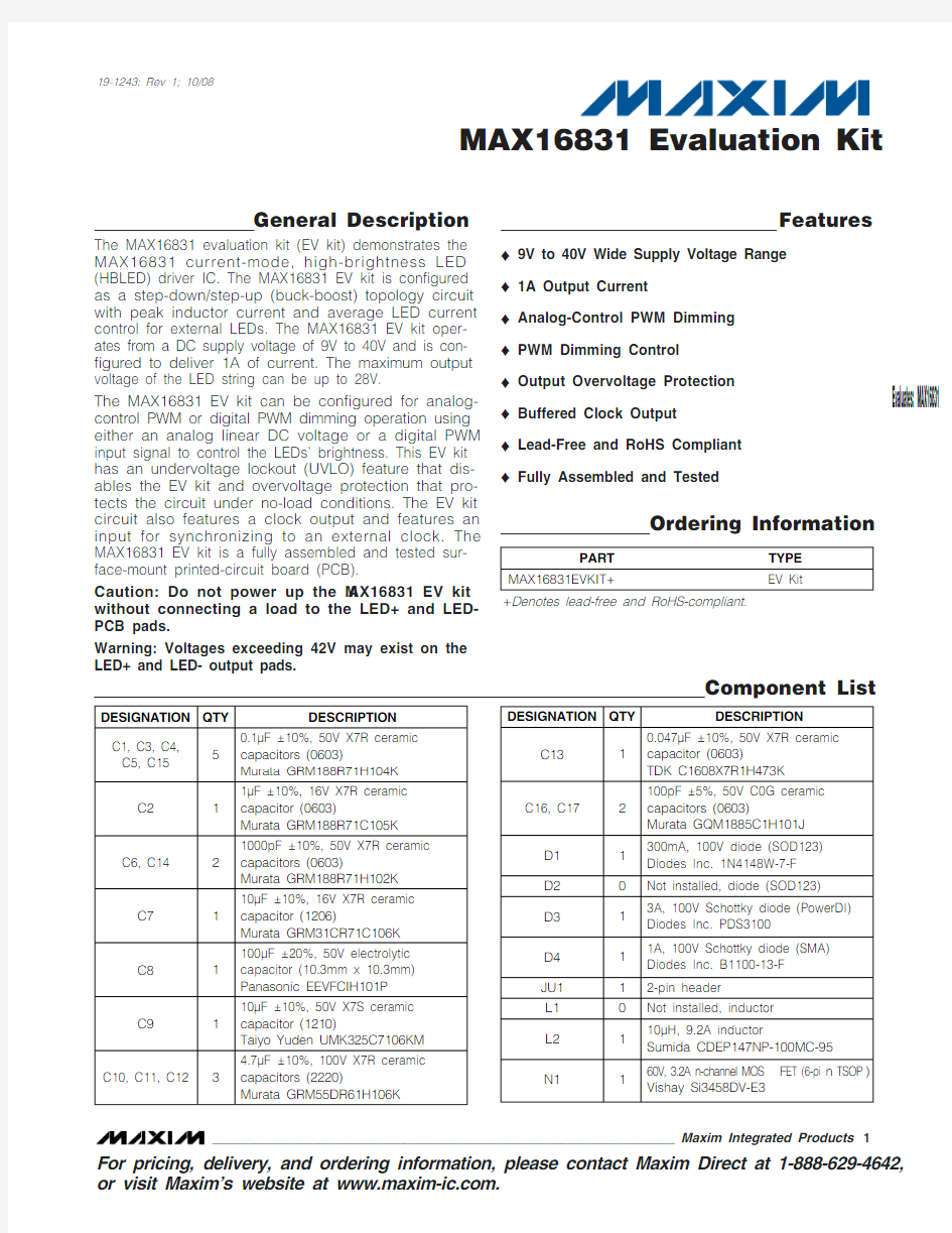
Component List
For pricing, delivery, and ordering information, please contact Maxim Direct at 1-888-629-4642,or visit Maxim’s website at https://www.doczj.com/doc/611044050.html,.
Ordering Information
+Denotes lead-free and RoHS-compliant.
E v a l u a t e s : M A X 16831
MAX16831 Evaluation Kit 2
_______________________________________________________________________________________
Quick Start
Recommended Equipment
Before beginning, the following equipment is needed:?9V to 40V, 4A power supply ?Two digital voltmeters
?A series-connected LED string rated at 1A (28V max)?A current probe to measure LED current
Procedures
The MAX16831 EV kit is fully assembled and tested.Follow the steps below to verify board operation.Caution: Do not turn on the power supply until all connections are completed and do not power up the M AX16831 EV kit without connecting a load to the LED+ and LED- PCB pads.
Warning: Voltages exceeding 42V may exist on the LED+ and LED- output pads.
1)Verify that a shunt is installed across jumper JU1(analog dimming control).2)Connect the power supply’s positive terminal to the V IN PCB pad on the EV kit. Connect the power sup-ply’s ground terminal to PGND PCB pad.3)Connect the digital voltmeters across the V IN and PGND PCB pads and the LED+ and LED-PCB pads.4)Connect the anode of the LED string to the LED+ pad.5)Connect the cathode of the LED string to the LED- pad.
Component List (continued)
6)Clip the current probe across the LED+ wire to mea-sure the LED current.7)Turn on the power supply and increase the input voltage to 9V.8)Adjust potentiometer R14 to obtain the desired LED current duty cycle.9)Measure the voltage between the LED+ and LED-PCB pads.
Detailed Description
The MAX16831 evaluation kit (EV kit) demonstrates the MAX16831 current-mode H BLED driver IC. The MAX16831 EV kit is configured in a step-down/step-up (buck-boost) topology with peak current control and average current control for a string of user-supplied external HBLEDs. The MAX16831 EV kit operates from a DC supply voltage of 9V to 40V and requires up to 4A.The circuit is configured to deliver 1A of current into series LED string with a maximum 28V forward voltage.The EV kit sets the maximum series inductor current to 8.3A using parallel resistors R6 and R7. The average LED current is set to 1A using resistor R3. A CLKOUT PCB pad is available to monitor the oscillator frequen-cy. A DIM PCB pad is also provided for PWM dimming operation of the external LEDs and to monitor the ana-log DC voltage applied at the MAX16831 IC DIM pin.
Undervoltage Lockout (UVLO)
The MAX16831 EV kit’s UVLO threshold is configured to 8.3V using resistors R1 and R2. The UVEN PCB pad can be used to disable the EV kit circuit by connecting UVEN to AGND. To configure the circuit to a different UVLO threshold, refer to the Setting the UVLO Threshold section in the MAX16831 IC data sheet.
Peak Inductor Current-Limit Setting
The parallel combination of current-sense resistors R6and R7 sets the EV kit’s peak inductor current limit to 8.3A. Use the following equation to calculate the total resistance needed to reconfigure the inductor peak current limit:
PEAK TOTAL the total parallel resistance placed at the R6 and R7PCB pads.
Refer to the ILIM and H ICCUP Comparator section in the MAX16831 IC data sheet for additional information on setting the peak current-limit threshold.
Setting External LED Current
Resistor R3 sets the MAX16831 EV kit average LED current to 1A. Use the following equation to calculate R3 when reconfiguring the LED current:
where I LED is the LED current.
LED Dimming Control
LED dimming can be achieved on the MAX16831 EV kit by applying a digital PWM signal or an analog DC volt-age at the DIM PCB input pad. Jumper JU1, poten-tiometer R14, resistor R15, and capacitor C15 configure the MAX16831 EV kit for analog-control PWM dimming operation.
Place a shunt across jumper JU1 to set the EV kit for analog-control PWM dimming and adjust potentiometer R14. The analog DC voltage at the DIM PCB pad sets the duty cycle of the LED current, which controls the external LED brightness. The MAX16831 IC DIM pin voltage can be monitored by placing a voltmeter across the DIM and AGND PCB pads.
Use the following equation to calculate the voltage at the DIM PCB pad, which is necessary to program the LED output current duty cycle, D:
where DIM is the analog DC voltage at the MAX16831EV kit DIM PCB pad in volts, and D is the duty cycle of the LED output current.
When operating the MAX16831 EV kit with analog-con-trol PWM dimming, the LED dimming frequency is inter-
nally set by the MAX16831 IC to 200Hz.
Remove the shunt at jumper JU1 to control LED dim-ming using a digital PWM signal at the DIM PCB pad.Apply a digital PWM signal with a 3.2V to 15V logic-high level in the 80H z to 2kH z frequency range and adjust the duty cycle to adjust the LED brightness. See Table 1 for jumper JU1 setting for LED dimming operation.
DIM D V V
?×+(.).2602Evaluates: MAX16831
MAX16831 Evaluation Kit
_______________________________________________________________________________________3
Table 1. MAX16831 LED Dimming
E v a l u a t e s : M A X 16831
CLK OUTPUT
The MAX16831 EV kit features a buffered digital clock output, CLKOUT. The MAX16831 PWM clock frequen-cy is programmed to 300kHz by resistor R13. To syn-chronize the MAX16831 EV kit to an external clock signal, connect a clock signal with a 2.8V to 5.5V logic level and 125kHz to 500kHz square wave at the RTSYNC PCB pad. Refer to the Oscillator, Clock, and Synchronization section in the MAX16831 IC data sheet for information on setting the MAX16831 IC PWM frequency.
Output Overvoltage Protection
The maximum voltage on the LED+ PCB pad is limited to 70.8V, with respect to GND, by a feedback network formed by resistors R9 and R10. When the voltage at LED+ exceeds the programmed 70.8V threshold,PWM switching is terminated and no further energy is transferred to the load connected between LED+ and LED-. Refer to the Setting the Overvoltage Threshold section in the MAX16831 IC data sheet for setting the overvoltage threshold.
If the EV kit is turned on with no load, the voltage at LED+ may rise to unsafe levels. Even though the EV kit has overvoltage protection, connect the speci-fied load before powering up the EV kit.
MAX16831 Evaluation Kit 4_______________________________________________________________________________________
Evaluates: MAX16831
MAX16831 Evaluation Kit
_______________________________________________________________________________________
5
Figure 1. MAX16831 EV Kit Schematic
E v a l u a t e s : M A X 16831
MAX16831 Evaluation Kit 6
_______________________________________________________________________________________
Figure 3. MAX16831 EV Kit PCB Layout—Component Side
Evaluates: MAX16831
MAX16831 Evaluation Kit
_______________________________________________________________________________________
7
Figure 5. MAX16831 EV Kit PCB Layout—VCC Layer 3
E v a l u a t e s : M A X 16831
MAX16831 Evaluation Kit 8
_______________________________________________________________________________________
Maxim cannot assume responsibility for use of any circuitry other than circuitry entirely embodied in a Maxim product. No circuit patent licenses are implied. Maxim reserves the right to change the circuitry and specifications without notice at any time.
Maxim Integrated Products, 120 San Gabriel Drive, Sunnyvale, CA 94086 408-737-7600 _____________________9?2008 Maxim Integrated Products is a registered trademark of Maxim Integrated Products, Inc.Evaluates: MAX16831
MAX16831 Evaluation Kit