?2000National Semiconductor Corporation https://www.doczj.com/doc/5512046613.html,
Geode?GXm Processor Integrated x86Solution with MMX Support
元器件交易网https://www.doczj.com/doc/5512046613.html,
https://www.doczj.com/doc/5512046613.html, 2Revision 3.1
G e o d e ?G X m P r o c e s s o r
Features
General Features
Packaged in:
—352-T erminal Ball Grid Array (BGA)or —320-Pin Staggered Pin Grid Array (SPGA)
0.35-micron four layer metal CMOS process Split rail design (3.3V I/O and 2.9V core)
32-Bit x86Processor
Supports the MMX instruction set extension for the
acceleration of multimedia applications
Speeds offered up to 266MHz 16KB unified L1cache
Integrated Floating Point Unit (FPU)
Re-entrant System Management Mode (SMM)
enhanced for VSA PCI Controller
Fixed,rotating,hybrid,or ping-pong arbitration Supports up to three PCI bus masters
Synchronous CPU and PCI bus clock frequency Supports concurrency between PCI master and L1
cache
Power Management
Designed to support CS5530power management
architecture
CPU only Suspend or full 3V Suspend supported:
—Clocks to CPU core stopped for CPU Suspend —All on-chip clocks stopped for 3V Suspend —Suspend refresh supported for 3V Suspend
Virtual Systems Architecture Technology
Architecture allows OS independent (software)virtual-
ization of hardware functions
Provides compatible high performance legacy VGA
core functionality
Note:GUI (Graphical User Interface)graphics accel-eration is pure hardware.
Provides 16-bit XpressAUDIO subsystem
2D Graphics Accelerator
Graphics pipeline performance significantly increased
over previous generations by pipelining burst reads/writes
Accelerates BitBLTs,line draw,text Supports all 256raster operations Supports transparent BLTs Runs at core clock frequency Full VGA and VESA mode support
Special "Driver level”instructions utilize internal
scratchpad for enhanced performance
Display Controller
Video Generator (VG)improves memory efficiency for
display refresh with SDRAM
Supports a separate MPEG1video buffer and data
path to enable video acceleration in the CS5530
Internal palette RAM for use with the CS5530 Direct interface to CS5530for CRT and TFT flat panel
support which eliminates need for external RAMDAC
Hardware frame buffer compressor/decompressor Hardware cursor
Supports up to 1280x1024x8bpp and 1024x768x16
bpp
XpressRAM Subsystem
Memory control/interface directly from CPU 64-Bit wide memory bus Support for:
—Two 168-pin unbuffered DIMMs
—Up to 16open banks simultaneously
—Single or 16-byte reads (burst length of two)
元器件交易网https://www.doczj.com/doc/5512046613.html,
Revision https://www.doczj.com/doc/5512046613.html,
Table of Contents
Geode?GXm Processor
1.0
Architecture Overview (8)
1.1INTEGER UNIT ...........................................................81.2FLOATING POINT UNIT ....................................................91.3WRITE-BACK CACHE UNIT .................................................91.4MEMORY MANAGEMENT UNIT ..............................................91.4.1Internal Bus Interface Unit ............................................91.5
INTEGRATED FUNCTIONS .................................................91.5.1Graphics Accelerator ................................................91.5.2Display Controller ..................................................101.5.3XpressRAM Memory Subsystem ......................................101.5.4PCI Controller .....................................................101.6
GEODE GXM/CS5530SYSTEM DESIGNS (11)
2.0Signal Definitions (13)
2.1PIN ASSIGNMENTS ......................................................132.2
SIGNAL DESCRIPTIONS ..................................................242.2.1System Interface Signals ............................................242.2.2PCI Interface Signals ...............................................262.2.3Memory Controller Interface Signals ...................................292.2.4Video Interface Signals .............................................302.2.5Power,Ground,and No Connect Signals ................................322.2.6Internal Test and Measurement Signals ................................322.3SUBSYSTEM SIGNAL CONNECTIONS .......................................342.4
POWER PLANES .........................................................
36
3.0Processor Programming (38)
3.1CORE PROCESSOR INITIALIZATION ........................................383.2INSTRUCTION SET OVERVIEW .............................................393.2.1Lock Prefix .......................................................393.3
REGISTER SETS .........................................................403.3.1Application Register Set .............................................403.3.2System Register Set ...............................................443.3.3Model Specific Register Set ..........................................593.3.4Time Stamp Counter ...............................................593.4
ADDRESS SPACES .......................................................603.4.1I/O Address Space .................................................603.4.2Memory Address Space .............................................603.5OFFSET,SEGMENT,AND PAGING MECHANISMS .............................613.6OFFSET MECHANISM ....................................................613.7
DESCRIPTORS AND SEGMENT MECHANISMS ................................623.7.1Real and Virtual 8086Mode Segment Mechanisms .......................623.7.2Segment Mechanism in Protective Mode ................................633.7.3GDTR and LDTR Registers ..........................................663.7.4Descriptor Bit Structure .............................................673.7.5Gate Descriptors ..................................................693.8MULTITASKING AND TASK STATE SEGMENTS ................................703.9
PAGING MECHANISM .....................................................
72
元器件交易网https://www.doczj.com/doc/5512046613.html,
https://www.doczj.com/doc/5512046613.html, 4Revision 3.1
Table of Contents (Continued)
G e o d e ?G X m P r o c e s s o r
3.10
INTERRUPTS AND EXCEPTIONS ...........................................743.10.1Interrupts ........................................................743.10.2Exceptions .......................................................743.10.3Interrupt Vectors ...................................................753.10.4Interrupt and Exception Priorities ......................................763.10.5Exceptions in Real Mode ............................................773.10.6Error Codes ......................................................773.11
SYSTEM MANAGEMENT MODE ............................................783.11.1SMM Enhancements ...............................................793.11.2SMM Operation ...................................................793.11.3The SMI#Pin .....................................................803.11.4SMM Configuration Registers ........................................803.11.5SMM Memory Space Header .........................................803.11.6SMM Instructions ..................................................823.11.7SMM Memory Space ...............................................833.11.8SMI Generation ...................................................833.11.9SMI Service Routine Execution .......................................833.12SHUTDOWN AND HALT ...................................................863.13
PROTECTION ...........................................................863.13.1Privilege Levels ...................................................863.13.2I/O Privilege Levels ................................................863.13.3Privilege Level Transfers ............................................873.13.4Initialization and Transition to Protected Mode ............................873.14
VIRTUAL 8086MODE .....................................................883.14.1Memory Addressing ................................................883.14.2Protection ........................................................883.14.3Interrupt Handling ..................................................883.14.4Entering and Leaving Virtual 8086Mode ................................883.15
FLOATING POINT UNIT OPERATIONS .......................................893.15.1FPU (Floating Point Unit)Register Set ..................................893.15.2FPU T ag Word Register .............................................893.15.3FPU Status Register ...............................................893.15.4FPU Mode Control Register ..........................................
89
4.0Integrated Functions (91)
4.1
INTEGRATED FUNCTIONS PROGRAMMING INTERFACE .......................924.1.1Graphics Control Register ...........................................924.1.2Control Registers ..................................................944.1.3Graphics Memory ..................................................944.1.4L1Cache Controller ................................................954.1.5Display Driver Instructions ...........................................984.1.6CPU_READ/CPU_WRITE Instructions .................................994.2
INTERNAL BUS INTERFACE UNIT ..........................................1004.2.1FPU Error Support ................................................1004.2.2A20M Support ...................................................1004.2.3SMI Generation ..................................................1004.2.4640KB to 1MB Region ............................................1004.2.5Internal Bus Interface Unit Registers . (101)
元器件交易网https://www.doczj.com/doc/5512046613.html,
Revision https://www.doczj.com/doc/5512046613.html,
Table of Contents (Continued)
Geode?GXm Processor
4.3
MEMORY CONTROLLER (103)
4.3.1Memory Array Configuration ........................................1044.3.2Memory Organizations .............................................1054.3.3SDRAM Commands ...............................................1064.3.4Memory Controller Register Description ...............................1084.3.5Address Translation ...............................................1124.3.6Memory Cycles ..................................................1154.3.7SDRAM Interface Clocking ..........................................1184.4
GRAPHICS PIPELINE ....................................................1204.4.1BitBLT/Vector Engine ..............................................1204.4.2Master/Slave Registers ............................................1214.4.3Pattern Generation ................................................1214.4.4Source Expansion ................................................1234.4.5Raster Operations ................................................1234.4.6Graphics Pipeline Register Descriptions ...............................1244.5
DISPLAY CONTROLLER ..................................................1294.5.1Display FIFO ....................................................1304.5.2Compression T echnology ...........................................1304.5.3Motion Video Acceleration Support ...................................1304.5.4Hardware Cursor .................................................1314.5.5Display Timing Generator ...........................................1314.5.6Dither and Frame-Rate Modulation ...................................1314.5.7Display Modes ...................................................1314.5.8Graphics Memory Map .............................................1354.5.9Display Controller Registers .........................................1364.5.10Memory Organization Registers ......................................1444.5.11Timing Registers .................................................1464.5.12Cursor Position Registers ...........................................1494.5.13Color Registers ..................................................1504.5.14Palette Access Registers ...........................................1514.5.15CS5530Display Controller Interface ..................................1534.6
PCI CONTROLLER ......................................................1554.6.1X-Bus PCI Slave ..................................................1554.6.2X-Bus PCI Master ................................................1554.6.3PCI Arbiter ......................................................1554.6.4Generating Configuration Cycles .....................................1554.6.5Generating Special Cycles ..........................................1554.6.6PCI Configuration Space Control Registers .............................1564.6.7PCI Configuration Space Registers ...................................1574.6.8PCI Cycles ......................................................
162
5.0Virtual Subsystem Architecture (165)
5.1VIRTUAL VGA (165)
5.1.1Traditional VGA Hardware ..........................................1655.2
GXM VIRTUAL VGA ......................................................1675.2.1Datapath Elements ................................................1675.2.2Video Refresh ...................................................1685.2.3GXm VGA Hardware ..............................................1685.2.4VGA Video BIOS .................................................1715.2.5Virtual VGA Register Descriptions ....................................
172
元器件交易网https://www.doczj.com/doc/5512046613.html,
https://www.doczj.com/doc/5512046613.html, 6Revision 3.1
Table of Contents (Continued)G e o d e ?G X m P r o c e s s o r
6.0
Power Management (174)
6.1APM SUPPORT .........................................................1746.2CPU SUSPEND COMMAND REGISTERS ....................................1746.3SUSPEND MODULATION .................................................1746.43-VOLT SUSPEND MODE .................................................1746.5
SUSPEND MODE AND BUS CYCLES .......................................1756.5.1Initiating Suspend with SUSP#......................................1756.5.2Initiating Suspend with HALT ........................................1766.5.3Responding to a PCI Access During Suspend Mode ......................1776.5.4Stopping the Input Clock ...........................................1786.6GXM PROCESSOR SERIAL BUS ..........................................1796.6.1Serial Packet Transmission .........................................1796.7
POWER MANAGEMENT REGISTERS .......................................
179
7.0Electrical Specifications (182)
7.1PART NUMBERS ........................................................1827.2
ELECTRICAL CONNECTIONS .............................................1827.2.1Power/Ground Connections and Decoupling ............................1827.2.2Power Sequencing the Core and I/O Voltages ...........................1827.2.3NC-Designated Pins ...............................................1827.2.4Pull-Up and Pull-Down Resistors .....................................1827.2.5Unused Input Pins ................................................1827.3ABSOLUTE MAXIMUM RATINGS ...........................................1837.4OPERATING CONDITIONS ................................................1847.5DC CHARACTERISTICS ..................................................1857.6
AC CHARACTERISTICS ..................................................
186
8.0Package Specifications (195)
8.1THERMAL CHARACTERISTICS ............................................1958.1.1Heatsink Considerations ...........................................1968.2
MECHANICAL PACKAGE OUTLINES (198)
9.0Instruction Set (201)
9.1
GENERAL INSTRUCTION SET FORMAT .....................................2029.1.1Prefix (Optional).................................................2039.1.2Opcode .........................................................2039.1.3mod and r/m Byte (Memory Addressing)...............................2059.1.4reg Field ........................................................2069.1.5s-i-b Byte (Scale,Indexing,Base)....................................2079.2
CPUID INSTRUCTION ....................................................2089.2.1Standard CPUID Levels ............................................2089.2.2Extended CPUID Levels ............................................2109.3PROCESSOR CORE INSTRUCTION SET ....................................2129.4FPU INSTRUCTION SET ..................................................2249.5MMX INSTRUCTION SET .................................................2299.6
NATIONAL SEMICONDUCTOR EXTENDED MMX INSTRUCTION SET .............
234
元器件交易网https://www.doczj.com/doc/5512046613.html,
Revision https://www.doczj.com/doc/5512046613.html,
Table of Contents (Continued)
Geode?GXm Processor
Appendix A Support Documentation (236)
A.1ORDER INFORMATION ..................................................236A.2
DATA BOOK REVISION HISTORY (236)
元器件交易网https://www.doczj.com/doc/5512046613.html,
https://www.doczj.com/doc/5512046613.html, 8Revision 3.1
G e o d e ?G X m P r o c e s s o r
元器件交易网https://www.doczj.com/doc/5512046613.html,
Revision https://www.doczj.com/doc/5512046613.html,
Architecture Overview (Continued )
Geode?GXm Processor
1.2
FLOATING POINT UNIT
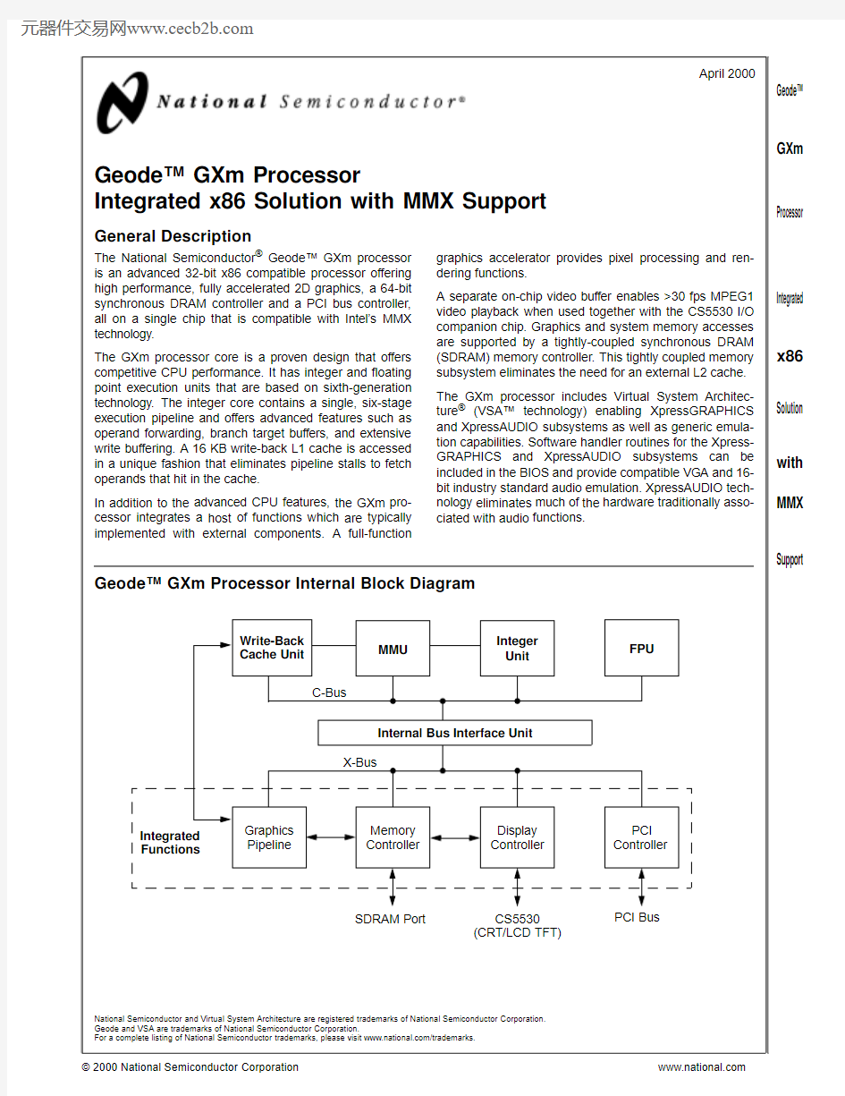
The FPU (Floating Point Unit)interfaces to the integer unit and the cache unit through a 64-bit bus.The FPU is x87-instruction-set compatible and adheres to the IEEE-754standard.Because almost all applications that contain FPU instructions also contain integer instructions,the GXm processor’s FPU achieves high performance by completing integer and FPU operations in parallel.FPU instructions are dispatched to the pipeline within the integer unit.The address calculation stage of the pipeline checks for memory management exceptions and accesses memory operands for use by the FPU.Once the instructions and operands have been provided to the FPU,the FPU completes instruction execution independently of the integer unit.
1.3WRITE-BACK CACHE UNIT
The 16KB write-back unified cache is a data/instruction cache and is configured as four-way set associative.The cache stores up to 16KB of code and data in 1024cache lines.
The GXm processor provides the ability to allocate a por-tion of the L1cache as a scratchpad,which is used to accelerate the Virtual Systems Architecture algorithms as well as for some graphics operations.
1.4MEMORY MANAGEMENT UNIT
The memory management unit (MMU)translates the lin-ear address supplied by the integer unit into a physical address to be used by the cache unit and the internal bus interface unit.Memory management procedures are x86-compatible,adhering to standard paging mechanisms.The MMU also contains a load/store unit that is responsi-ble for scheduling cache and external memory accesses.The load/store unit incorporates two performance-enhancing features:
?Load-store reordering that gives priority to memory reads required by the integer unit over writes to external memory.?Memory-read bypassing that eliminates unnecessary memory reads by using valid data from the execution unit.1.4.1Internal Bus Interface Unit
The internal bus interface unit provides a bridge from the GXm processor to the integrated system functions (i.e.,memory subsystem,display controller,graphics pipeline)and the PCI bus interface.
When external memory access is required,the physical address is calculated by the memory management unit and then passed to the internal bus interface unit,which translates the cycle to an X-Bus cycle (the X-Bus is a National Semiconductor proprietary internal bus which provides a common interface for all of the system mod-ules).The X-Bus memory cycle now is arbitrated between
other pending X-Bus memory requests to the SDRAM controller before completing.
In addition,the internal bus interface unit provides config-uration control for up to 20different regions within system memory with separate controls for read access,write access,cacheability,and PCI access.
1.5INTEGRATED FUNCTIONS
The GXm processor integrates the following functions tra-ditionally implemented using external devices:?High-performance 2D graphics accelerator ?Separate CRT and TFT data paths from the display controller ?SDRAM memory controller
?PCI bridge
The processor has also been enhanced to support National Semiconductor’s proprietary Virtual System Architecture (VSA)implementation.
The GXm processor implements a Unified Memory Archi-tecture (UMA).By using National Semiconductor’s Dis-play Compression Technology (DCT),the performance degradation inherent in traditional UMA systems is elimi-nated.
1.5.1Graphics Accelerator
The graphics accelerator is a full-featured GUI (Graphical User Interface)accelerator.The graphics pipeline imple-ments a bitBLT engine for frame buffer bitBLTs and rect-angular fills.Additional instructions in the integer unit may be processed,as the bitBLT engine assists the CPU in the bitBLT operations that take place between system mem-ory and the frame buffer.This combination of hardware and software is used by the display driver to provide very fast transfers in both directions between system memory and the frame buffer.The bitBLT engine also draws ran-domly-oriented vectors,and scanlines for polygon fill.All of the pipeline operations described in the following list can be applied to any bitBLT operation.
?Pattern Memory.Render with 8x8dither,8x8mono-chrome,or 8x1color pattern.?Color Expansion.Expand monochrome bitmaps to full-depth 8-or 16-bit colors.?Transparency.Suppresses drawing of background pixels for transparent text.?Raster Operations.Boolean operation combines source,destination,and pattern bitmaps.
元器件交易网https://www.doczj.com/doc/5512046613.html,
https://www.doczj.com/doc/5512046613.html, 10Revision 3.1
Architecture Overview (Continued )
G e o d e ?G X m P r o c e s s o r
1.5.2Display Controller
The display port is a direct interface to the CS5530which drives a TFT flat panel display,LCD panel,or a CRT dis-play.
The display controller (video generator)retrieves image data from the frame buffer region of memory,performs a color-look-up if required,inserts the cursor overlay into the pixel stream,generates display timing,and formats the pixel data for output to a variety of display devices.The display controller contains Display Compression Technology (DCT)that allows the GXm processor to refresh the display from a compressed copy of the frame buffer.DCT typically decreases the screen-refresh band-width requirement by a factor of 15to 20,further minimiz-ing bandwidth contention.
1.5.3XpressRAM Memory Subsystem
The memory controller drives a 64-bit SDRAM port directly.The SDRAM memory array contains both the main system memory and the graphics frame buffer.Up to four module banks of SDRAM are supported.Each mod-ule bank will have two or four component banks depend-ing on the memory size and organization.The maximum configuration is four module banks with four component banks providing a total of 16open banks.The maximum memory size is 1GB.
The memory controller handles multiple requests for memory data from the GXm processor,the graphics accelerator and the display controller.The memory con-troller contains extensive buffering logic that helps mini-mize contention for memory bandwidth between graphics and CPU requests.The memory controller cooperates with the internal bus controller to determine the cacheabil-ity of all memory references.
1.5.4PCI Controller
The GXm processor incorporates a full-function PCI inter-face module that includes the PCI arbiter.All accesses to external I/O devices are sent over the PCI bus,although most memory accesses are serviced by the SDRAM con-troller.The Internal Bus Interface Unit contains address mapping logic that determines if memory accesses are targeted for the SDRAM or for the PCI bus.
元器件交易网https://www.doczj.com/doc/5512046613.html,
Revision https://www.doczj.com/doc/5512046613.html,
Architecture Overview (Continued )
Geode?GXm Processor
1.6
GEODE GXM/CS5530SYSTEM DESIGNS
The GXm Integrated Subsystem with MMX support con-sists of two chips,the GXm Processor and the CS5530I/O companion.The subsystem provides high perfor-mance using 32-bit x86processing.The two chips inte-grate video,audio and memory interface functions normally performed by external hardware.
As described in separate manuals,the CS5530enables the full features of the GXm processor with MMX support.These features include full VGA and VESA video,16-bit stereo sound,IDE interface,ISA interface,SMM power
management,and A T compatibility logic.In addition,the newer CS5530provides an Ultra DMA/33interface,MPEG2assist,and AC97Version 2.0compliant audio.Figure 1-2shows a basic block system diagram (refer to Figure 2-4on page 34for detailed subsystem intercon-nection signals).It includes the National Semiconductor CS9210Dual-Scan Flat Panel Display Controller for designs that need to interface to a DSTN panel (instead of TFT panel).
Figure 1-2.Geode?GXm/CS5530System Block Diagram
YUV Port (Video)
RGB Port PCI Interface
SDRAM MD[63:0]
PCI Bus
Geode?CS5530I/O Companion
Graphics Data Video Data
Analog RGB
Digital RGB (to TFT or DSTN Panel)CRT
TFT Panel
USB (2Ports)
AC97Codec
Speakers
CD ROM Audio
Micro-phone
GPIO
Port (Graphics)
Super ISA Bus
SDRAM
Serial Packet
Clocks
I/O
BIOS
IDE Devices
14.31818MHz Crystal
IDE Control
System Clocks
DC-DC &Battery
CS9210DSTN Controller
DSTN Panel
Geode?GXm Processor
Geode?元器件交易网https://www.doczj.com/doc/5512046613.html,
https://www.doczj.com/doc/5512046613.html, 12Revision 3.1
Architecture Overview (Continued )
G e o d e ?G X m P r o c e s s o r
The CS9210converts the digital RGB output of the CS5530I/O companion chip to the digital output suitable for driving a dual-scan color STN (DSTN)flat panel LCD.It connects to the digital RGB output of a GXm processor or 55x 0and drives the graphics data onto a dual-scan flat
panel LCD.It can drive all standard dual-scan color STN flat panels up to 1024x768resolution.Figure 1-3shows an example of a CS9210interface in a typical GXm Inte-grated Subsystem.
Figure 1-3.CS9210Interface System Diagram
DRAM Data Address Control 13
16
Panel Control 624
Panel Data
DSTN Pixel Port
24
Pixel Data
LCD
18
CS5530CS9210DSTN Controller
I/O
DRAM-B 256Kx16Bit
DRAM-A 256Kx16Bit
Address Control 13DRAM Data
16
4
Serial
Configuration
Companion
(Control &Data)
Geode?GXm Processor
Geode?Geode?元器件交易网https://www.doczj.com/doc/5512046613.html,
Revision https://www.doczj.com/doc/5512046613.html,
Geode?GXm Processor
2.0
Signal Definitions
This section describes the external interface of the Geode GXm processor.Figure 2-1shows the signals organized by their functional interface groups (internal test and elec-trical pins are not shown).
2.1PIN ASSIGNMENTS
The tables in this section use several common abbrevia-tions.Table 2-1lists the mnemonics and their meanings.Figure 2-2on page 14shows the pin assignment for the 352BGA with Tables 2-2and 2-3listing the pin assign-ments sorted by pin number and alphabetically by signal name,respectively.
Figure 2-3on page 19shows the pin assignment for the 320SPGA with Tables 2-4and 2-5listing the pin assign-ments sorted by pin number and alphabetically by signal name,respectively.
In Section 2.2“Signal Descriptions”starting on Page 24a description of each signal is provided within its associated functional group.
Following the signal descriptions,information regarding subsystem signal connections and split power planes and decoupling is provided..
Figure 2-1.Functional Block Diagram
Table 2-1.Pin Type Definitions
Mnemonic
Definition
I Standard input pin.I/O Bidirectional pin.O T otem-pole output.
OD
Open-drain output structure that allows multiple devices to share the pin in a wired-OR configuration PU Pull-up resistor PD Pull-down resistor
s/t/s
Sustained tri-state,an active-low tri-state signal owned and driven by one and only one agent at a time.The agent that drives an s/t/s pin low must drive it high for at least one clock before letting it float.A new agent cannot start driving an s/t/s signal any sooner than one clock after the previous owner lets it float.A pull-up resistor is required to sustain the inactive state until another agent drives it,and must be provided by the central resource.VCC (PWR)Power pin.VSS (GND)Ground pin
#The "#"symbol at the end of a signal name indicates that the active,or
asserted state occurs when the signal is at a low voltage level.When "#"is not present after the signal name,the signal is asserted when at a high voltage level.
SYSCLK CLKMODE[2:0]
RESET INTR IRQ13SMI#SUSP#SUSPA#SERIALP
AD[31:0]C/BE[3:0]#
PAR FRAME#IRDY#TRDY#STOP#LOCK#DEVSEL#PERR#SERR#REQ[2:0]#GNT[2:0]#
MD[63:0]MA[12:0]BA[1:0]
RASA#,RASB#CASA#,CASB#CS[3:0]#
WEA#,WEB#DQM[7:0]CKEA,CKEB SDCLK[3:0]SDCLK_IN SDCLK_OUT PCLK VID_CLK DCLK
CRT_HSYNC CRT_VSYNC FP_VSYNC FP_HSYNC ENA_DISP VID_RDY VID_VAL
VID_DA TA[7:0]PIXEL[17:0]
Memory Controller Interface Video Interface Signals
PCI Interface Signals
System Interface Signals
Signals
Geode?GXm Processor
元器件交易网https://www.doczj.com/doc/5512046613.html,
https://www.doczj.com/doc/5512046613.html, 14Revision 3.1
Signal Definitions (Continued )
G e o d e ?G X m P r o c e s s o r
Figure 2-2.352BGA Pin Assignment Diagram
For order information refer to Section A.1“Order Information”on page 236.
1234567891011121314151617181920212223242526
A
B
C
D E
F G
H J
K L
M
N
P
R
T
U
V W
Y AA
AB AC
AD AE
AF
Index Corner
VSS
VSS AD27AD24AD21AD16VCC2FRAM#DEVS#VCC3PERR#AD15VSS
AD11CBE0#AD6
VCC2
AD4
AD2VCC3
AD0
AD1TEST2MD2
VSS VSS
VSS
VSS
AD28AD25AD22AD18VCC2CBE2#TRDY#VCC3LOCK#PAR
AD14AD12
AD9
AD7VCC2INTR AD3
VCC3TEST1TEST3MD1
MD33
VSS VSS
AD29AD31AD30AD26AD23AD19VCC2AD17IRDY#VCC3STOP#SERR#CBE1#AD13AD10
AD8
VCC2
AD5SMI#VCC3TEST0IRQ13MD32MD34MD3MD35
GNT0#
TDI REQ2#VSS CBE3#VSS
VCC2
VSS
VSS
VCC3
VSS
VSS
VSS
VSS
VSS
VSS VCC2
VSS
VSS VCC3
VSS
MD0
VSS MD4MD36TDN
GNT2#SUSPA#REQ0#AD20
MD6TDP MD5MD37
TD0GNT1#TEST
VSS
VSS
MD38
MD7
MD39
VCC3VCC3VCC3VCC3
VCC3VCC3VCC3VCC3
TMS SUSP#REQ1#VSS
VSS MD8
MD40
MD9
FPVSY TCLK RESET VSS
VSS
MD41MD10MD42
VCC2VCC2VCC2VCC2
VCC2VCC2VCC2VCC2
CKM1FPHSYSERLP VSS
VSS
MD11MD43MD12
CKM2VIDVAL CKM0
VSS VSS MD44MD13MD45
VSS
PIX1
PIX0VSS VSS MD14MD46MD15
VIDCLK PIX3
PIX2VSS VSS MD47CASA#SYSCLK
PIX4
PIX5PIX6VSS VSS
WEB#WEA#CASB#
PIX7
PIX8
PIX9
VSS
VSS DQM0DQM4DQM1
VCC3VCC3VCC3VCC3
VCC3VCC3VCC3VCC3
PIX10PIX11PIX12
VSS VSS DQM5CS2#CS0#
PIX13CRTHS PIX14
VSS
VSS RASA#RASB#MA0
VCC2VCC2VCC2VCC2
VCC2VCC2VCC2VCC2
PIX15PIX16CRTVS VSS
VSS MA1MA2MA3
DCLK PIX17VDA T6VDA T7
MA4
MA5MA6MA7
PCLK FLT#VDA T4VSS VOLDET VSS
VCC2
VSS
VSS
VCC3
VSS
VSS
VSS
VSS
VSS
VSS
VCC2
VSS
VSS
VCC3
VSS DQM6VSS
MA8
MA9MA10
VRDY VDA T5VDA T3VDA T0EDISP MD63VCC2MD62MD29VCC3MD59MD26MD56MD55MD22CKEB VCC2MD51MD18VCC3MD48DQM3CS1#MA11
BA0BA1
VSS
VSS VDA T2SCLK3SCLK1RWCLK VCC2SCKIN MD61VCC3MD28MD58MD25MD24MD54MD21VCC2MD20MD50VCC3MD17DQM7CS3#MA12VSS VSS
VSS
VSS VDA T1SCLK0SCLK2MD31VCC2SCKOUTMD30VCC3MD60MD27MD57
VSS
MD23MD53VCC2MD52MD19VCC3MD49MD16DQM2CKEA
VSS
VSS
1
2
3
4
5
6
7
8
9
10
11
12
13
14
15
16
17
18
19
20
21
22
23
24
25
26
A B
C D
E F
G H
J K
L
M
N
P
R T
U V
W Y
AA AB
AC AD
AE AF
Geode?GXm 352BGA -Top View
Note:Signal names have been abbreviated in this figure due to space constraints.
=GND terminal
=PWR terminal (VCC2=VCC_CORE;VCC3=VCC_IO)
Processor 元器件交易网https://www.doczj.com/doc/5512046613.html,
Revision https://www.doczj.com/doc/5512046613.html,
Signal Definitions (Continued )
Geode?GXm Processor
Table 2-2.352BGA Pin Assignments -Sorted by Pin Number
Pin No.
Signal Name
A1VSS A2VSS A3AD27A4AD24A5AD21A6AD16A7VCC2A8FRAME#A9DEVSEL#A10VCC3A11PERR#A12AD15A13VSS A14AD11A15C/BE0#A16AD6A17VCC2A18AD4A19AD2A20VCC3A21AD0A22AD1A23TEST2A24MD2A25VSS A26VSS B1VSS B2VSS B3AD28B4AD25B5AD22B6AD18B7VCC2B8C/BE2#B9TRDY#B10VCC3B11LOCK#B12P AR B13AD14B14AD12B15AD9B16AD7B17VCC2B18INTR B19AD3B20VCC3B21TEST1B22TEST3
B23MD1B24MD33B25VSS B26VSS C1AD29C2AD31C3AD30C4AD26C5AD23C6AD19C7VCC2C8AD17C9IRDY#C10VCC3C11STOP#C12SERR#C13C/BE1#C14AD13C15AD10C16AD8C17VCC2C18AD5C19SMI#C20VCC3C21TEST0C22IRQ13C23MD32C24MD34C25MD3C26MD35D1GNT0#D2TDI D3REQ2#D4VSS D5C/BE3#D6VSS D7VCC2D8VSS D9VSS D10VCC3D11VSS D12VSS D13VSS D14VSS D15VSS D16VSS D17VCC2D18VSS
Pin No.
Signal Name
D19VSS D20VCC3D21VSS D22MD0D23VSS D24MD4D25MD36D26TDN E1GNT2#E2SUSP A#E3REQ0#E4AD20E23MD6E24TDP E25MD5E26MD37F1TDO F2GNT1#F3TEST F4VSS F23VSS F24MD38F25MD7F26MD39G1VCC3G2VCC3G3VCC3G4VCC3G23VCC3G24VCC3G25VCC3G26VCC3H1TMS H2SUSP#H3REQ1#H4VSS H23VSS H24MD8H25MD40H26MD9J1FP_VSYNC J2TCLK J3RESET J4VSS J23VSS J24MD41J25MD10J26MD42
Pin No.
Signal Name
K1VCC2K2VCC2K3VCC2K4VCC2K23VCC2K24VCC2K25VCC2K26VCC2L1CLKMODE1L2FP_HSYNC L3SERIALP L4VSS L23VSS L24MD11L25MD43L26MD12M1CLKMODE2M2VID_VAL M3CLKMODE0M4VSS M23VSS M24MD44M25MD13M26MD45N1VSS N2PIXEL1N3PIXEL0N4VSS N23VSS N24MD14N25MD46N26MD15P1VID_CLK P2PIXEL3P3PIXEL2P4VSS P23VSS P24MD47P25CASA#P26SYSCLK R1PIXEL4R2PIXEL5R3PIXEL6R4VSS R23VSS R24WEB#R25WEA#R26CASB#
Pin No.
Signal Name
T1PIXEL7T2PIXEL8T3PIXEL9T4VSS T23VSS T24DQM0T25DQM4T26DQM1U1VCC3U2VCC3U3VCC3U4VCC3U23VCC3U24VCC3U25VCC3U26VCC3V1PIXEL10V2PIXEL11V3PIXEL12V4VSS V23VSS V24DQM5V25CS2#V26CS0#W1PIXEL13W2CRT_HSYNC W3PIXEL14W4VSS W23VSS W24RASA#W25RASB#W26MA0Y1VCC2Y2VCC2Y3VCC2Y4VCC2Y23VCC2Y24VCC2Y25VCC2Y26VCC2AA1PIXEL15AA2PIXEL16AA3CRT_VSYNC AA4VSS AA23VSS AA24MA1AA25MA2AA26MA3
Pin No.
Signal Name
元器件交易网https://www.doczj.com/doc/5512046613.html,
https://www.doczj.com/doc/5512046613.html, 16Revision 3.1
Signal Definitions (Continued )
G e o d e ?G X m P r o c e s s o r
AB1DCLK AB2PIXEL17AB3VID_DAT A6AB4VID_DAT A7AB23MA4AB24MA5AB25MA6AB26MA7AC1PCLK AC2FLT#AC3VID_DAT A4AC4VSS AC5VOLDET AC6VSS AC7VCC2AC8VSS AC9VSS AC10VCC3AC11VSS AC12VSS AC13VSS AC14VSS AC15VSS
Pin No.
Signal Name
AC16VSS AC17VCC2AC18VSS AC19VSS AC20VCC3AC21VSS AC22DQM6AC23VSS AC24MA8AC25MA9AC26MA10AD1VID_RDY AD2VID_DAT A5AD3VID_DAT A3AD4VID_DAT A0AD5ENA_DISP AD6MD63AD7VCC2AD8MD62AD9MD29AD10VCC3AD11MD59AD12MD26
Pin No.
Signal Name
AD13MD56AD14MD55AD15MD22AD16CKEB AD17VCC2AD18MD51AD19MD18AD20VCC3AD21MD48AD22DQM3AD23CS1#AD24MA11AD25BA0AD26BA1AE1VSS AE2VSS AE3VID_DAT A2AE4SDCLK3AE5SDCLK1AE6RW_CLK AE7VCC2AE8SDCLK_IN AE9MD61
Pin No.
Signal Name
AE10VCC3AE11MD28AE12MD58AE13MD25AE14MD24AE15MD54AE16MD21AE17VCC2AE18MD20AE19MD50AE20VCC3AE21MD17AE22DQM7AE23CS3#AE24MA12AE25VSS AE26VSS AF1VSS AF2VSS AF3VID_DAT A1AF4SDCLK0AF5SDCLK2AF6MD31
Pin No.
Signal Name
AF7VCC2AF8SDCLK_OUT AF9MD30AF10VCC3AF11MD60AF12MD27AF13MD57AF14VSS AF15MD23AF16MD53AF17VCC2AF18MD52AF19MD19AF20VCC3AF21MD49AF22MD16AF23DQM2AF24CKEA AF25VSS AF26VSS
Pin No.
Signal Name
Table 2-2.
352BGA Pin Assignments -Sorted by Pin Number (Continued)
元器件交易网https://www.doczj.com/doc/5512046613.html,
Revision https://www.doczj.com/doc/5512046613.html,
Signal Definitions (Continued )
Geode?GXm Processor
Table 2-3.352BGA Pin Assignments -Sorted Alphabetically by Signal Name
Signal Name Type Pin No.AD0I/O A21AD1I/O A22AD2I/O A19AD3I/O B19AD4I/O A18AD5I/O C18AD6I/O A16AD7I/O B16AD8I/O C16AD9I/O B15AD10I/O C15AD11I/O A14AD12I/O B14AD13I/O C14AD14I/O B13AD15I/O A12AD16I/O A6AD17I/O C8AD18I/O B6AD19I/O C6AD20I/O E4AD21I/O A5AD22I/O B5AD23I/O C5AD24I/O A4AD25I/O B4AD26I/O C4AD27I/O A3AD28I/O B3AD29I/O C1AD30I/O C3AD31I/O C2BA0O AD25BA1O AD26CASA#O P25CASB#O R26C/BE0#I/O A15C/BE1#I/O C13C/BE2#I/O B8C/BE3#I/O D5CKEA O AF24CKEB O AD16CLKMODE0I M3CLKMODE1I L1CLKMODE2I M1CRT_HSYNC O W2CRT_VSYNC O AA3CS0#O V26CS1#O AD23CS2#O V25CS3#O AE23DCLK I AB1DEVSEL#
s/t/s
A9(PU)
DQM0O T24DQM1O T26DQM2O AF23DQM3O AD22DQM4O T25DQM5O V24DQM6O AC22DQM7O AE22ENA_DISP O AD5FLT#I AC2FP_HSYNC O L2FP_VSYNC O J1FRAME#s/t/s A8(PU)GNT0#O D1GNT1#O F2GNT2#O E1INTR I B18IRDY#s/t/s C9(PU)IRQ13O C22LOCK#s/t/s B11(PU)MA0O W26MA1O AA24MA2O AA25MA3O AA26MA4O AB23MA5O AB24MA6O AB25MA7O AB26MA8O AC24MA9O AC25MA10O AC26MA11O AD24MA12O AE24MD0I/O D22MD1I/O B23MD2I/O A24MD3I/O C25MD4I/O D24MD5I/O E25MD6I/O E23MD7I/O F25MD8I/O H24MD9I/O H26MD10I/O J25MD11I/O L24MD12I/O L26MD13I/O M25MD14I/O N24MD15I/O N26MD16I/O AF22MD17I/O AE21MD18I/O AD19MD19
I/O
AF19
Signal Name Type Pin No.MD20I/O AE18MD21I/O AE16MD22I/O AD15MD23I/O AF15MD24I/O AE14MD25I/O AE13MD26I/O AD12MD27I/O AF12MD28I/O AE11MD29I/O AD9MD30I/O AF9MD31I/O AF6MD32I/O C23MD33I/O B24MD34I/O C24MD35I/O C26MD36I/O D25MD37I/O E26MD38I/O F24MD39I/O F26MD40I/O H25MD41I/O J24MD42I/O J26MD43I/O L25MD44I/O M24MD45I/O M26MD46I/O N25MD47I/O P24MD48I/O AD21MD49I/O AF21MD50I/O AE19MD51I/O AD18MD52I/O AF18MD53I/O AF16MD54I/O AE15MD55I/O AD14MD56I/O AD13MD57I/O AF13MD58I/O AE12MD59I/O AD11MD60I/O AF11MD61I/O AE9MD62I/O AD8MD63I/O AD6PAR I/O B12PCLK O AC1PERR#s/t/s A11(PU)PIXEL0O N3PIXEL1O N2PIXEL2O P3PIXEL3O P2PIXEL4O R1PIXEL5
O
R2
Signal Name Type Pin No.PIXEL6O R3PIXEL7O T1PIXEL8O T2PIXEL9O T3PIXEL10O V1PIXEL11O V2PIXEL12O V3PIXEL13O W1PIXEL14O W3PIXEL15O AA1PIXEL16O AA2PIXEL17O AB2RASA#O W24RASB#O W25REQ0#I E3(PU)REQ1#I H3(PU)REQ2#I D3(PU)RESET I J3RW_CLK O AE6SDCLK_IN I AE8SDCLK_OUT O AF8SDCLK0O AF4SDCLK1O AE5SDCLK2O AF5SDCLK3O AE4SERIALP O L3SERR#OD C12(PU)SMI#I C19STOP#s/t/s C11(PU)SUSP#I H2(PU)SUSPA#O E2SYSCLK I P26TCLK I J2(PU)TDI I D2(PU)TDN O D26TDO O F1TDP O E24TEST I F3(PD)TEST0O C21TEST1O B21TEST2O A23TEST3O B22TMS I H1(PU)TRDY#s/t/s B9(PU)VCC2PWR A7VCC2PWR A17VCC2PWR B7VCC2PWR B17VCC2PWR C7VCC2PWR C17VCC2PWR D7VCC2PWR D17VCC2
PWR
K1
Signal Name Type Pin No.元器件交易网https://www.doczj.com/doc/5512046613.html,
https://www.doczj.com/doc/5512046613.html, 18Revision 3.1
Signal Definitions (Continued )
G e o d e ?G X m P r o c e s s o r
Note:PU/PD indicates pin is
internally connected to a 20-kohm pull-up/-down resistor.
VCC2PWR K2VCC2PWR K3VCC2PWR K4VCC2PWR K23VCC2PWR K24VCC2PWR K25VCC2PWR K26VCC2PWR Y1VCC2PWR Y2VCC2PWR Y3VCC2PWR Y4VCC2PWR Y23VCC2PWR Y24VCC2PWR Y25VCC2PWR Y26VCC2PWR AC7VCC2PWR AC17VCC2PWR AD7VCC2PWR AD17VCC2PWR AE7VCC2PWR AE17VCC2PWR AF7VCC2PWR AF17VCC3PWR A10VCC3PWR A20VCC3PWR B10VCC3PWR B20VCC3PWR C10VCC3PWR C20VCC3PWR D10VCC3PWR D20VCC3PWR G1VCC3PWR G2VCC3PWR G3VCC3PWR G4VCC3PWR G23VCC3
PWR
G24
Signal Name Type Pin No.VCC3PWR G25VCC3PWR G26VCC3PWR U1VCC3PWR U2VCC3PWR U3VCC3PWR U4VCC3PWR U23VCC3PWR U24VCC3PWR U25VCC3PWR U26VCC3PWR AC10VCC3PWR AC20VCC3PWR AD10VCC3PWR AD20VCC3PWR AE10VCC3PWR AE20VCC3PWR AF10VCC3PWR AF20VID_CLK O P1VID_DATA0O AD4VID_DATA1O AF3VID_DATA2O AE3VID_DATA3O AD3VID_DATA4O AC3VID_DATA5O AD2VID_DATA6O AB3VID_DATA7O AB4VID_RDY I AD1VID_VAL O M2VOLDET O AC5VSS GND A1VSS GND A2VSS GND A13VSS GND A25VSS GND A26VSS GND B1VSS
GND
B2
Signal Name Type Pin No.VSS GND B25VSS GND B26VSS GND D4VSS GND D6VSS GND D8VSS GND D9VSS GND D11VSS GND D12VSS GND D13VSS GND D14VSS GND D15VSS GND D16VSS GND D18VSS GND D19VSS GND D21VSS GND D23VSS GND F4VSS GND F23VSS GND H4VSS GND H23VSS GND J4VSS GND J23VSS GND L4VSS GND L23VSS GND M4VSS GND M23VSS GND N1VSS GND N4VSS GND N23VSS GND P4VSS GND P23VSS GND R4VSS GND R23VSS GND T4VSS GND T23VSS GND V4VSS
GND
V23
Signal Name Type Pin No.VSS GND W4VSS GND W23VSS GND AA4VSS GND AA23VSS GND AC4VSS GND AC6VSS GND AC8VSS GND AC9VSS GND AC11VSS GND AC12VSS GND AC13VSS GND AC14VSS GND AC15VSS GND AC16VSS GND AC18VSS GND AC19VSS GND AC21VSS GND AC23VSS GND AE1VSS GND AE2VSS GND AE25VSS GND AE26VSS GND AF1VSS GND AF2VSS GND AF14VSS GND AF25VSS GND AF26WEA#O R25WEB#
O
R24
Signal Name Type Pin No.Table 2-3.
352BGA Pin Assignments -Sorted Alphabetically by Signal Name (Continued)
元器件交易网https://www.doczj.com/doc/5512046613.html,
Revision https://www.doczj.com/doc/5512046613.html,
Signal Definitions (Continued )
Geode?GXm Processor
Figure 2-3.320SPGA Pin Assignment Diagram
For order information refer to Section A.1“Order Information”on page 236.
1
23
45
67
89
1011121314151617181920212223242526A B C D E F G H J K L M N P Q R S T U V AA AB AC AD AE AF Index Corner
2728293031323334353637
AG AH AJ AK AL AM W Y X Z AN
A B C D E F
G H J K L M N P Q R S T
U V AA AB AC AD
AE AF AG AH AJ AK AL AM W Y X Z AN
12345678910111213141516171819202122232425262728293031323334353637
VCC3
AD25
VSS
VCC2
AD16
VCC3
STOP#
SERR#
VSS
AD11AD8
VCC3
AD2
VCC2VSS
TST0VCC3
VSS
VSS AD27CBE3#AD21AD19CBE2#TRDY#LOCK#CBE1#AD13
AD9
AD6
AD3
SMI#
AD1
TST2
MD33MD2
VCC3
AD31
AD26AD23VCC2AD18FRAME#VSS PAR VCC3AD10
VSS
AD4
AD0VCC2IRQ13MD1
MD34VCC3AD30AD29AD24
AD22AD20AD17IRDY#PERR#AD14
AD12AD7
INTR
TST1TST3
MD0
MD32
MD3
MD35
REQ0#
REQ2#
AD28VSS
VCC2VCC2VSS
DEVSEL#AD15VSS
CBE0#AD5VSS
VCC2VCC2VSS
MD4
MD36TDN GNT0#
TDI
MD5
TDP
VSS CLKMODE2VSS
VSS MD37VSS
GNT2#SUSPA#
TDO
VSS TEST
REQ1#GNT1#
VCC2
VCC2VCC2
RESET SUSP#
VCC3
TMS VSS FPVSYN TCK
SERIALP
VSS
NC
CKMD1FPHSYN CKMD0VID_VAL
PIX0
PIX1
PIX2
VSS VCC3VSS PIX3
VID_CLK PIX6
PIX5
PIX4
NC
PIX9
PIX8
VSS
PIX7NC PIX10VCC3PIX11
VSS
PIX12PIX13
VCC2
VCC2VCC2
CRTHSYN DCLK PIX14
VSS
VCC2
PIX15PIX16
VSS
PIX17
VSS
CRTVSYN VDAT6MD6
MD38VCC2
VSS
MD7
MD39MD8
VCC2
VCC2VCC2
MD40MD9
VSS
MD41VCC3
MD10
MD42MD11
VSS
MD43MD44
MD12
MD14MD13
MD45
MD15MD46
VSS
VCC3
VSS
SYSCLK MD47
WEA#
WEB#CASA#
DQM0CASB#
DQM1
VSS
DQM4
CS2#DQM5
VSS
CS0#
VCC3
RASB#RASA#
VCC2
VCC2
VCC2
VCC2
VSS
MA1MA2MA0
MA4MA3
VSS MA5VSS MA8
MA6
MA10
PCLK
FLT#
VDAT5VSS
VCC2
MD31
VSS
MD60MD57
VSS
MD22MD52
VSS
VCC2VCC2
VSS
BA1
MA9MA7VRDY VSS
VDAT0SDCLK0SDCLK2SDCLKIN
MD29
MD27MD56
MD55
MD21
MD20MD50
MD16DQM3
CS3#
VSS BA0VCC2
VDA T4VDAT2SDCLK1VCC2
RWCLK SDCLKOUT VSS
MD58VCC3MD23
VSS
MD19MD49VCC2DQM6CKEA
MA11
VCC3
VDAT7VDAT3ENDIS SDCLK3MD63MD30
MD61
MD59
MD25
MD24MD53
MD51
MD18MD48DQM7DQM2MA12VOLDET
VSS
VCC2VDAT1VSS VCC2MD62VCC3MD28MD26VSS
MD54CKEB VCC3MD17VCC2VSS CS1#VCC3
VSS
Note:Signal names have been abbreviated in this figure due to space constraints.
=Denotes GND terminal
=Denotes PWR terminal (VCC2=VCC_CORE;VCC3=VCC_IO)
320SPGA -Top View
Processor
Geode?GXm 元器件交易网https://www.doczj.com/doc/5512046613.html,
https://www.doczj.com/doc/5512046613.html, 20Revision 3.1
Signal Definitions (Continued )
G e o d e ?G X m P r o c e s s o r
Table 2-4.320SPGA Pin Assignments -Sorted by Pin Number
Pin No.
Signal Name
A3VCC3A5AD25A7VSS A9VCC2A11AD16A13VCC3A15STOP#A17SERR#A19VSS A21AD11A23AD8A25VCC3A27AD2A29VCC2A31VSS A33TEST0A35VCC3A37VSS B2VSS B4AD27B6C/BE3#B8AD21B10AD19B12C/BE2#B14TRDY#B16LOCK#B18C/BE1#B20AD13B22AD9B24AD6B26AD3B28SMI#B30AD1B32TEST2B34MD33B36MD2C1VCC3C3AD31C5AD26C7AD23C9VCC2C11AD18C13FRAME#C15VSS C17P AR C19VCC3C21AD10C23VSS
C25AD4C27AD0C29VCC2C31IRQ13C33MD1C35MD34C37VCC3D2AD30D4AD29D6AD24D8AD22D10AD20D12AD17D14IRDY#D16PERR#D18AD14D20AD12D22AD7D24INTR D26TEST1D28TEST3D30MD0D32MD32D34MD3D36MD35E1REQ0#E3REQ2#E5AD28E7VSS E9VCC2E11VCC2E13VSS E15DEVSEL#E17AD15E19VSS E21C/BE0#E23AD5E25VSS E27VCC2E29VCC2E31VSS E33MD4E35MD36E37TDN F2GNT0#F4TDI F34MD5F36TDP
Pin No.
Signal Name
G1VSS G3CLKMODE2G5VSS G33VSS G35MD37G37VSS H2GNT2#H4SUSP A#H34MD6H36MD38J1TDO J3VSS J5TEST J33VCC2J35VSS J37MD7K2REQ1#K4GNT1#K34MD39K36MD8L1VCC2L3VCC2L5VCC2L33VCC2L35VCC2L37VCC2M2RESET M4SUSP#M34MD40M36MD9N1VCC3N3TMS N5VSS N33VSS N35MD41N37VCC3P2FP_VSYNC P4TCLK P34MD10P36MD42Q1SERIALP Q3VSS Q5NC Q33MD11Q35VSS Q37MD43R2CLKMODE1R4FP_HSYNC
Pin No.
Signal Name
R34MD44R36MD12S1CLKMODE0S3VID_VAL S5PIXEL0S33MD14S35MD13S37MD45T2PIXEL1T4PIXEL2T34MD15T36MD46U1VSS U3VCC3U5VSS U33VSS U35VCC3U37VSS V2PIXEL3V4VID_CLK V34SYSCLK V36MD47W1PIXEL6W3PIXEL5W5PIXEL4W33WEA#W35WEB#W37CASA#X2NC X4PIXEL9X34DQM0X36CASB#Y1PIXEL8Y3VSS Y5PIXEL7Y33DQM1Y35VSS Y37DQM4Z2NC Z4PIXEL10Z34CS2#Z36DQM5AA1VCC3AA3PIXEL11AA5VSS AA33VSS AA35CS0#AA37VCC3
Pin No.
Signal Name
AB2PIXEL12AB4PIXEL13AB34RASB#AB36RASA#AC1VCC2AC3VCC2AC5VCC2AC33VCC2AC35VCC2AC37VCC2AD2CRT_HSYNC AD4DCLK AD34MA2AD36MA0AE1PIXEL14AE3VSS AE5VCC2AE33VCC2AE35VSS AE37MA1AF2PIXEL15AF4PIXEL16AF34MA4AF36MA3AG1VSS AG3PIXEL17AG5VSS AG33VSS AG35MA5AG37VSS
AH2CRT_VSYNC AH4VID_DAT A6AH32MA10AH34MA8AH36MA6AJ1PCLK AJ3FTL#AJ5VID_DAT A5AJ7VSS AJ9VCC2AJ11MD31AJ13VSS AJ15MD60AJ17MD57AJ19VSS AJ21MD22AJ23MD52AJ25VSS
Pin No.
Signal Name
元器件交易网https://www.doczj.com/doc/5512046613.html,