
Features
l Surface Mount Application l 11 thru 200 Volt Voltage Range l Built-in strain relief l Glass passivated junction l Low inductance
Mechanical Data
l
Case: JEDEC DO-214AB Molded plastic
over passivated junction
l Terminals solderable per MIL-STD-750, Method 2026 l Standard Packaging: 16mm tape(EIA-481)
l Maximum temperature for soldering: 260o
C for 10 seconds. l Plastic package has Underwriters Laboratory
Flammability Classification 94V-O
Maximum Ratings @ 25o C Unless Otherwise Specified DC Power Dissipation P D 5.0W Pea k forward Surge Curr ent 8.3ms sin gle half
I FS M See
Fig.5 (Note:1 ,2)
Operation And Storage Temperature T J , T STG -55o C to +150 o C NOTES:
1. Mounted on 8.0mm copper pads to each terminal.
2. 8.3ms single half sine-wave, or equivalent square wave,duty cycle = 4 pulses per minute maximum.
2
omp onents 21201 Itasca Street Chatsworth
! "# $ % ! "#
(Note: 1 )
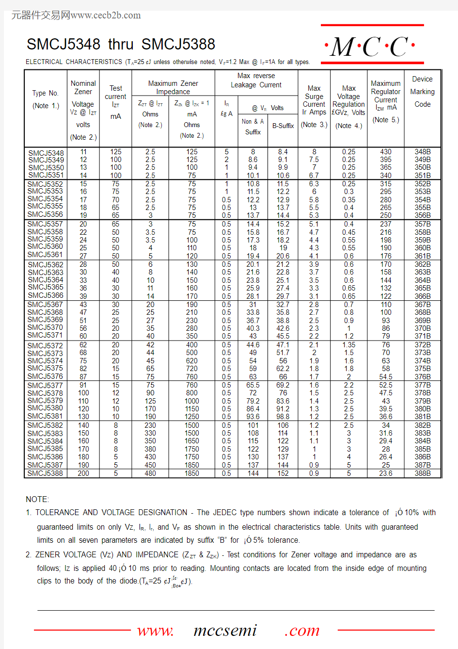
ELECTRICAL CHARACTERISTICS (T A =25¢J unless otherwise noted, V F =1.2 Max @ I F =1A for all types.
Maximum Zener Impedance
Max reverse Leakage Current
@ V R
Volts
Type No.(Note 1.)
Nominal Zener Voltage Vz @ I ZT volts (Note 2.)
T est current I ZT mA
Z ZT @ I ZT Ohms (Note 2.)
Z Zk @ I ZK = 1
mA Ohms (Note 2.)
I R
£g A
Non & A
Suffix
B-Suffix Max Surge Current Ir Amps (Note 3.)Max Voltage Regulation £G Vz, Volts
(Note 4.)
Maximum
Regulator Current I ZM mA (Note 5.)Device Marking Code
11121314125100100100 2.52.52.52.512512510075521188.69.410.18.49.19.910.687.576.70.250.250.250.25430395365340348B 349B 350B 351B 15161718197575706565 2.52.52.52.537575757575110.50.50.510.811.512.21313.711.512.212.913.714.4 6.365.85.55.30.250.30.350.40.4315295280265250352B 353B 354B 355B 356B 2022242527655050505033.53.54575751001101200.50.50.50.50.514.415.817.31819.415.216.718.21920.6 5.14.74.44.34.10.40.450.550.550.6237216198190176357B 358B 359B 360B 361B 28303336395040403030681011141301401501601700.50.50.50.50.520.121.623.825.928.121.222.825.127.429.7 3.93.73.53.33.10.60.60.60.650.65170158144132122362B 363B 364B 365B 366B 4347515660302525202020252735401902102302803500.50.50.50.50.53133.836.740.34332.735.838.842.645.5 2.82.72.52.32.20.70.80.911.2110100938679367B 368B 369B 370B 371B 6268758287202020151542444565754005006207207600.50.50.50.50.544.64954596347.151.75662.266 2.121.91.81.7 1.351.51.61.827670635854.5372B 373B 374B 375B 376B 91100110120130151212101075901251701907608001000115012500.50.50.50.50.565.57279.286.493.669.27683.691.298.8 1.61.51.41.31.2 2.22.52.52.52.552.547.54339.536.6377B 378B 379B 380B 381B 1401501601701801908888552303303503804304501500150016501750175018500.50.50.50.50.50.5101108115122130137106114122129137144 1.21.11.1110.9 2.5333453431.629.42826.425382B 383B 384B 385B 386B 387B 200548018500.51441520.9523.6388B
NOTE:
1. TOLERANCE AND VOLTAGE DESIGNATION - The JEDEC type numbers shown indicate a tolerance of ?ó10% with guaranteed limits on only Vz, I R , I r , and V F as shown in the electrical characteristics table. Units with guaranteed limits on all seven parameters are indicated by suffix “B” for ?ó5% tolerance.
2. ZENER VOLTAGE (Vz) AND IMPEDANCE (Z ZT & Z ZK ) - T est conditions for Zener voltage and impedance are as follows; Iz is applied 40?ó10 ms prior to reading. Mounting contacts are located from the inside edge of mounting clips to the body of the diode.(T A =25¢J ??¢·
?D¢±¢J ).
SMCJ5348SMCJ5351SMCJ5350SMCJ5349SMCJ5352SMCJ5355SMCJ5354SMCJ5353SMCJ5356SMCJ5357SMCJ5360SMCJ5359SMCJ5358SMCJ5361SMCJ5362SMCJ5365SMCJ5364SMCJ5363SMCJ5366SMCJ5367SMCJ5370SMCJ5369SMCJ5368SMCJ5371SMCJ5372SMCJ5375SMCJ5374SMCJ5373SMCJ5376SMCJ5377SMCJ5380SMCJ5379SMCJ5378SMCJ5381SMCJ5382SMCJ5385SMCJ5384SMCJ5383SMCJ5386SMCJ5387SMCJ5388
3. SURGE CURRENT (Ir) - Surge current is specified as the maximum allowable peak, non-recurrent square-wave
current with a pulse width, PW, of 8.3 ms. The data given in Figure 5 may be used to find the maximum surge current for a quare wave of any pulse width between 1 ms and 1000ms by plotting the applicable points on
logarithmic paper. Examples of this, using the 6.8v and 200V zeners, are shown in Figure 6. Mounting
contact located as specified in Note 3. (T A=25¢J??¢·
?D¢±
¢J).
4. VOLTAGE REGULATION (£G Vz) - Test conditions for voltage regulation are as follows: Vz measurements are made
at 10% and then at 50% of the Iz max value listed in the electrical characteristics table. The test currents are the same for the 5% and 10% tolerance devices. The test current time druation for each Vz measurement is 40?ó10 ms.
(T A=25¢J??¢·
?D¢±
¢J). Mounting contact located as specified in Note2.
5. MAXIMUM REGULATOR CURRENT (I ZM) - The maximum current shown is based on the maximum voltage of a
5% type unit. Therefore, it applies only to the B-suffix device. The actual I ZM for any device may not exceed the value of 5 watts divided by the actual Vz of the device. T L=75¢J at maximum from the device body.
APPLICATION NOTE:
Since the actual voltage available from a given zener diode is temperature dependent, it is necessary to determine junction temperature under any set of operating conditions in order to calculate its value. The following procedure is recommended:
Lead Temperature, T L, should be determined from:
T L = £c LA P D + T A
£c LA is the lead-to-ambient thermal resistance (¢J/W) and P D is the power dissipation.
Junction Temperature, T J , may be found from:
T J = T L + £G T JL
£G T JL is the increase in junction temperature above the lead temperature and may be found from Figure 3 for a train of power pulses or from Figure 4 for dc power.
£G T JL = £c JL P D
For worst-case design, using expected limits of Iz, limits of P D and the extremes of T J(£G T J) may be estimated. Changes in voltage, Vz, can then be found from:
£G V= £c VZ£G T J
£c VZ, the zener voltage temperature coefficient, is fount from Figures 2.
Under high power-pulse operation, the zener voltage will vary with time and may also be affected significantly be the zener resistance. For best regulation, keep current excursions as low as possible.
Data of Figure 3 should not be used to compute surge capability. Surge limitations are given in Figure 5. They are lower than would be expected by considering only junction temperature, as current crowding effects cause temperatures to be extremely high in small spots resulting in device degradation should the limits of Figure. 5 be exceeded.
RATING AND CHARACTERISTICS CURVES
TEMPERATURE COEFFICIENTS
TL, LEAD TEMPERATURE (¢J )
VZ, ZENER VOLTAGE @IZT (VOLTS)
Fig. 1-POWER TEMPERATURE DERATING CURVE
Fig. 2-TEMPERATURE COEFFICIENT-RANGE FOR UNITS
6 TO 220 VOLTS
TIME (SECONDS)
Fig. 3-TYPICAL THERMAL RESPONSE
L, LEAD LENGTH TO HEAT SINK (INCH)
NOMINAL VZ(V)
Fig. 4-TYPICAL THERMAL RESISTANCE
Fig. 5-MAXIMUM NON-REPETITIVE SURGE
CURRENT VERSUS NOMINAL ZENER
VOLTAGE (SEE NOTE 3)
SM C J5348 thru SM C J5388
RATING AND CHARACTERISTICS CURVES
ZENER VOLTAGE VERSUS ZENER CURRENT
(FIGURES 7,8, AND 9)
1
10
100
1000
1000
1001010.11
2
3
4
5
6
7
8
9
10
VZ, ZENER VOLTAGE (VOLTS)
Fig. 6-PEAK SURGE CURRENT VERSUS PULSE
WIDTH(SEE NOTE 3)
Fig. 7-ZENER VOLTAGE VERSUS ZENER CURRENT
VZ = 6.8 THRU 10 VOLTS
0.1
50 60
80
VZ, ZENER VOLTAGE (VOLTS)
0.1
VZ, ZENER VOLTAGE (VOLTS)
Fig. 8-ZENER VOLTAGE VERSUS ZENER CURRENT
VZ = 11 THRU 75 VOLTS Fig. 9-ZENER VOLTAGE VERSUS ZENER CURRENT
VZ = 82 THRU 200 VOLTS
*** Data of Figure 3 should not be used to compute surge capability. Surge limitations are given in Figure 5. They are
lower than would be expected by considering only junction temperature, as current crowding effects cause
temperatures to be extremely high in small spots resulting in device degradation should the limits of Figure. 5 be exceeded
SM C J5348 thru SM C J5388