Cascadable Silicon Bipolar MMIC?Amplifier Technical Data
Features
?Cascadable 50 ? Gain Block ? 3 dB Bandwidth:DC to 0.7 GHz ?High Gain:
18.0 dB Typical at 0.5?GHz ?Low Noise Figure:3.0 dB Typical at 0.5?GHz ?Low Cost Surface Mount Plastic Package ?Tape-and-Reel Packaging Option Available [1]
MSA-0611
SOT-143 Package
Description
The MSA-0611 is a low cost silicon bipolar Monolithic Microwave Integrated Circuit (MMIC) housed in the surface mount plastic SOT-143 package. This MMIC is designed for use as a general purpose 50 ? gain block. Typical applications include narrow and broad band IF and RF amplifiers in commercial and industrial applications.
The MSA-series is fabricated using HP’s 10 GHz f T , 25?GHz f MAX ,silicon bipolar MMIC process which uses nitride self-alignment,ion implantation, and gold metalli-zation to achieve excellent
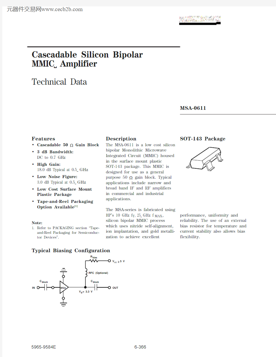
Typical Biasing Configuration
R
V CC > 5 V
IN
OUT
Note:
1.Refer to PACKAGING section “Tape-and-Reel Packaging for Semiconduc-tor Devices”.
performance, uniformity and reliability. The use of an external bias resistor for temperature and current stability also allows bias flexibility.
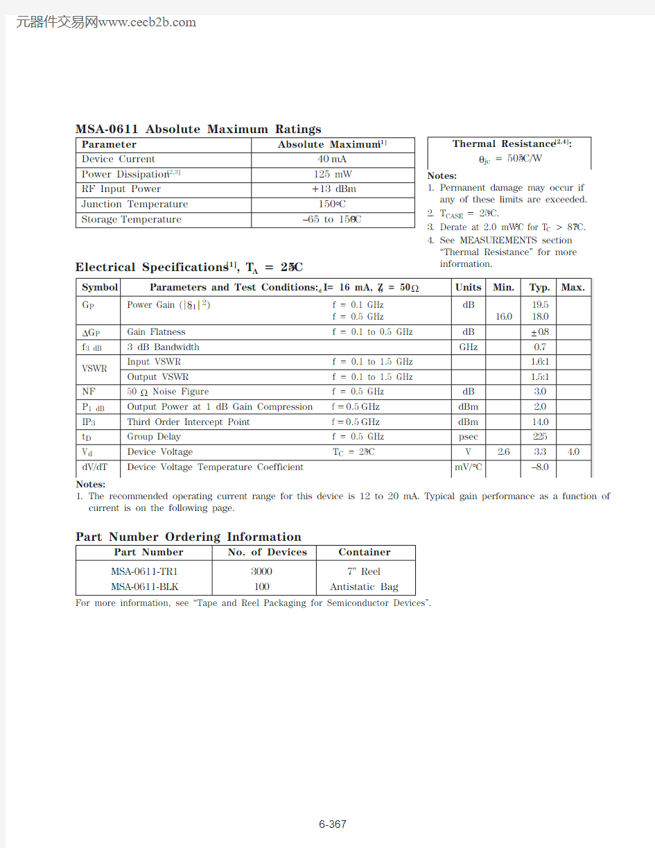
MSA-0611 Absolute Maximum Ratings
Parameter Absolute Maximum [1]
Device Current
40 mA Power Dissipation [2,3]125 mW RF Input Power
+13 dBm Junction Temperature 150°C Storage Temperature
–65 to 150°C
Thermal Resistance [2,4]:
θjc = 505°C/W
Notes:
1.Permanent damage may occur if any of these limits are exceeded.
2.T CASE = 25°C.
3.Derate at 2.0 mW/°C for T C > 87°C.
4.See MEASUREMENTS section “Thermal Resistance” for more information.
Part Number Ordering Information
Part Number No. of Devices
Container MSA-0611-TR130007" Reel MSA-0611-BLK
100
Antistatic Bag
For more information, see “Tape and Reel Packaging for Semiconductor Devices”.
Electrical Specifications [1], T A = 25°C
Symbol
Parameters and Test Conditions: I d = 16 mA, Z O = 50 ?
Units
Min.
Typ.
Max.
G P Power Gain (|S 21|2) f = 0.1 GHz dB
19.5f = 0.5 GHz 16.0
18.0?G P Gain Flatness f = 0.1 to 0.5 GHz
dB ±0.8f 3 dB 3 dB Bandwidth GHz
0.7I nput VSWR f = 0.1 to 1.5 GHz 1.6:1Output VSWR f = 0.1 to 1.5 GHz 1.5:1
NF 50 ? Noise Figure
f = 0.5 GHz dB 3.0P 1 dB Output Power at 1 dB Gain Compression f = 0.5 GHz dBm 2.0IP 3Third Order Intercept Point f = 0.5 GHz dBm 14.0t D Group Delay f = 0.5 GHz psec 225V d Device Voltage
T C = 25°C V 2.6
3.3
4.0
dV/dT
Device Voltage Temperature Coefficient
mV/°C
–8.0
Notes:
1.The recommended operating current range for this device is 12 to 20 mA. Typical gain performance as a function of current is on the following page.
VSWR
Typical Performance, T A = 25°C
(unless otherwise noted)
G p (d B )
N F (d B )
FREQUENCY (GHz)
T A 0
3691215
18
21Figure 4. Noise Figure vs. Frequency,I d = 16 mA.
0.1
2.5
3.03.5
4.0
0.5 1.0 2.0
0.20.3MSA-0611 Typical Scattering Parameters (Z O = 50 ?, T A = 25°C, I d = 16 mA)
Freq.GHz
Mag
Ang
dB
Mag
Ang
dB
Mag
Ang
Mag
Ang
k
0.1.04–17619.69.53170–23.0.0716.04–57 1.070.2.03–16319.39.25160–22.7.07310.07–82 1.070.3.03–14918.98.79150–22.8.07214.09–97 1.100.4.04–13218.58.38141–21.9.08017.11–111 1.070.5.05–12718.07.96133–21.6.08321.13–122 1.070.6.07–12317.37.33125–21.2.08723.15–131 1.070.8.10–12916.2 6.46111–19.7.10325.17–147 1.041.0.13–13915.0 5.6498–19.0.11228.18–160 1.061.5.22–16412.5 4.2273–17.1.13925.19175 1.072.0.3117110.1 3.2053–16.1.15721.19160 1.132.5.391588.1 2.5542–15.4.16922.20153 1.193.0.45144 6.3 2.0728–15.0.17818.19150 1.263.5.50132 4.7 1.7216–14.6.18515.16152 1.334.0.52121 3.4 1.484–14.1.19711.14166 1.37
A model for this device is available in the DEVICE MODELS section.
S 11S 21S 12 S 22
SOT-143 Package Dimensions
DIMENSIONS ARE IN MILLIMETERS (INCHES)