https://www.doczj.com/doc/579832674.html,
FEATURES DESCRIPTION
APPLICATIONS
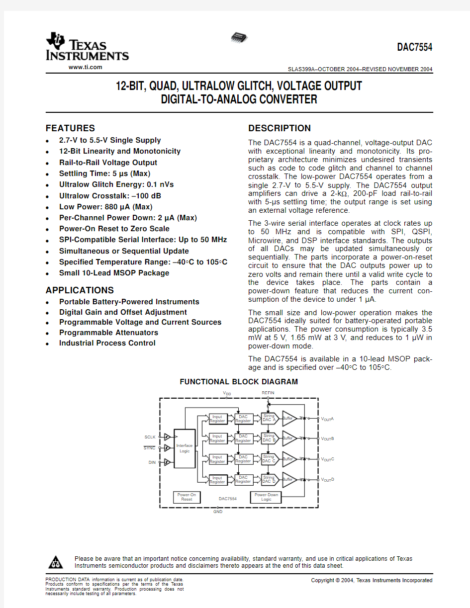
SCLK
SYNC
DIN
OUT A
OUT B
OUT C
OUT D
DAC7554
SLAS399A–OCTOBER2004–REVISED NOVEMBER2004 12-BIT,QUAD,ULTRALOW GLITCH,VOLTAGE OUTPUT
DIGITAL-TO-ANALOG CONVERTER
? 2.7-V to5.5-V Single Supply The DAC7554is a quad-channel,voltage-output DAC
with exceptional linearity and monotonicity.Its pro-?12-Bit Linearity and Monotonicity
prietary architecture minimizes undesired transients ?Rail-to-Rail Voltage Output
such as code to code glitch and channel to channel ?Settling Time:5μs(Max)crosstalk.The low-power DAC7554operates from a ?Ultralow Glitch Energy:0.1nVs single2.7-V to5.5-V supply.The DAC7554output
amplifiers can drive a2-k?,200-pF load rail-to-rail ?Ultralow Crosstalk:–100dB
with5-μs settling time;the output range is set using ?Low Power:880μA(Max)an external voltage reference.
?Per-Channel Power Down:2μA(Max)
The3-wire serial interface operates at clock rates up ?Power-On Reset to Zero Scale to50MHz and is compatible with SPI,QSPI,?SPI-Compatible Serial Interface:Up to50MHz Microwire,and DSP interface standards.The outputs
of all DACs may be updated simultaneously or ?Simultaneous or Sequential Update
sequentially.The parts incorporate a power-on-reset ?Specified Temperature Range:–40°C to105°C circuit to ensure that the DAC outputs power up to
?Small10-Lead MSOP Package zero volts and remain there until a valid write cycle to
the device takes place.The parts contain a
power-down feature that reduces the current con-
sumption of the device to under1μA.
?Portable Battery-Powered Instruments
?Digital Gain and Offset Adjustment The small size and low-power operation makes the
DAC7554ideally suited for battery-operated portable ?Programmable Voltage and Current Sources
applications.The power consumption is typically3.5?Programmable Attenuators
mW at5V,1.65mW at3V,and reduces to1μW in ?Industrial Process Control power-down mode.
The DAC7554is available in a10-lead MSOP pack-
age and is specified over–40°C to105°C.
FUNCTIONAL BLOCK DIAGRAM
Please be aware that an important notice concerning availability,standard warranty,and use in critical applications of Texas
Instruments semiconductor products and disclaimers thereto appears at the end of this data sheet.
https://www.doczj.com/doc/579832674.html,
ABSOLUTE MAXIMUM RATINGS
DAC7554
SLAS399A–OCTOBER 2004–REVISED NOVEMBER 2004This integrated circuit can be damaged by ESD.Texas Instruments recommends that all integrated circuits be handled with appropriate precautions.Failure to observe proper handling and installation procedures can cause damage.
ESD damage can range from subtle performance degradation to complete device failure.Precision integrated circuits may be more susceptible to damage because very small parametric changes could cause the device not to meet its published specifications.
ORDERING INFORMATION
SPECIFIED PACKAGE
PACKAGE ORDERING TRANSPORT PRODUCT PACKAGE TEMPERATURE
DESIGNATOR MARKING NUMBER MEDIA RANGE
DAC7554IDGS 80-piece Tube DAC755410MSOP DGS –40°C TO 105°C D754DAC7554IDGSR 2500-piece Tape
and Reel
over operating free-air temperature range (unless otherwise noted)(1)
UNIT
V DD to GND
–0.3V to 6V Digital input voltage to GND
–0.3V to V DD +0.3V V out to GND
–0.3V to V DD +0.3V Operating temperature range
–40°C to 105°C Storage temperature range
–65°C to 150°C Junction temperature (T J Max)
150°C (1)Stresses above those listed under “Absolute Maximum Ratings”may cause permanent damage to the device.Exposure to absolute
maximum conditions for extended periods may affect device reliability.
https://www.doczj.com/doc/579832674.html,
ELECTRICAL CHARACTERISTICS
DAC7554 SLAS399A–OCTOBER2004–REVISED NOVEMBER2004
V DD =2.7V to5.5V,REFIN=VDD,R
L
=2k?to GND;C
L
=200pF to GND;all specifications–40°C to105°C,unless
otherwise specified
PARAMETER TEST CONDITIONS MIN TYP MAX UNITS STATIC PERFORMANCE(1)
Resolution12Bits Relative accuracy±0.35±1LSB Differential nonlinearity Specified monotonic by design±0.08±0.5LSB Offset error±12mV
Zero-scale error All zeroes loaded to DAC register±12mV
Gain error±0.15%FSR Full-scale error±0.5%FSR Zero-scale error drift7μV/°C Gain temperature coefficient3ppm of FSR/°C PSRR V DD=5V0.75mV/V OUTPUT CHARACTERISTICS(2)
Output voltage range0REFIN V Output voltage settling time R L=2k?;0pF Slew rate1V/μs Capacitive load stability R L=∞470pF R L=2k?1000 Digital-to-analog glitch impulse1LSB change around major carry0.1nV-s Channel-to-channel crosstalk1-kHz full-scale sine wave,outputs unloaded–100dB Digital feedthrough0.1nV-s Output noise density(10-kHz offset fre-70nV/rtHz quency) Total harmonic distortion F OUT=1kHz,F S=1MSPS,BW=20kHz–85dB DC output impedance1? Short-circuit current V DD=5V50mA V DD=3V20 Power-up time Coming out of power-down mode,V DD=5V15μs Coming out of power-down mode,V DD=3V15 LOGIC INPUTS(2) Input current±1μA V IN_L,Input low voltage V DD=5V0.3V DD V V IN_H,Input high voltage V DD=3V0.7V DD V Pin capacitance3pF POWER REQUIREMENTS V DD 2.7 5.5V I DD(normal operation)DAC active and excluding load current V DD=3.6V to5.5V V IH=V DD and V IL=GND700880μA V DD=2.7V to3.6V550830 I DD(all power-down modes) V DD=3.6V to5.5V V IH=V DD and V IL=GND0.22μA V DD=2.7V to3.6V0.052 Reference input impedance25k?POWER EFFICIENCY I OUT/I DD I LOAD=2mA,V DD=5V93% (1)Linearity tested using a reduced code range of48to4048;output unloaded. (2)Specified by design and characterization,not production tested. https://www.doczj.com/doc/579832674.html, TIMING CHARACTERISTICS(1)(2) SCLK SYNC D IN DAC7554 SLAS399A–OCTOBER2004–REVISED NOVEMBER2004 V DD =2.7V to5.5V,R L =2k?to GND;all specifications–40°C to105°C,unless otherwise specified PARAMETER TEST CONDITIONS MIN TYP MAX UNITS V DD=2.7V to3.6V20 t1(3)SCLK cycle time ns V DD=3.6V to5.5V20 V DD=2.7V to3.6V10 t2SCLK HIGH time ns V DD=3.6V to5.5V10 V DD=2.7V to3.6V10 t3SCLK LOW time ns V DD=3.6V to5.5V10 V DD=2.7V to3.6V4 SYNC falling edge to SCLK falling edge setup t4ns time V DD =3.6V to5.5V4 V DD=2.7V to3.6V5 t5Data setup time ns V DD=3.6V to5.5V5 V DD=2.7V to3.6V 4.5 t6Data hold time ns V DD=3.6V to5.5V 4.5 V DD=2.7V to3.6V0 t7SCLK falling edge to SYNC rising edge ns V DD=3.6V to5.5V0 V DD=2.7V to3.6V20 t8Minimum SYNC HIGH time ns V DD=3.6V to5.5V20 (1)All input signals are specified with t R=t F=1ns(10%to90%of V DD)and timed from a voltage level of(V IL+V IH)/2. (2)See Serial Write Operation timing diagram Figure1. (3)Maximum SCLK frequency is50MHz at V DD=2.7V to5.5V. Figure1.Serial Write Operation https://www.doczj.com/doc/579832674.html, PIN DESCRIPTION V OUT V OUT V OUT V OUT DAC7554 SLAS399A–OCTOBER2004–REVISED NOVEMBER2004 DGS Package (Top View) Terminal Functions TERMINAL DESCRIPTION https://www.doczj.com/doc/579832674.html, 1VOUTA Analog output voltage from DAC A 2VOUTB Analog output voltage from DAC B 3GND Ground 4VOUTC Analog output voltage from DAC C 5VOUTD Analog output voltage from DAC D 6SCLK Serial clock input 7DIN Serial data input 8VDD Analog voltage supply input 9SYNC Frame synchronization input.The falling edge of the FS pulse indicates the start of a serial data frame shifted out to the DAC7554 10REFIN Analog input.External reference https://www.doczj.com/doc/579832674.html, TYPICAL CHARACTERISTICS L i n e a r i t y E r r o r ? L S B D i f f e r e n t i a l L i n e a r i t y E r r o r ? L S B Digital Input Code 05121024153620482560307235844096 L i n e a r i t y E r r o r ? L S B D i f f e r e n t i a l L i n e a r i t y E r r o r ? L S B Digital Input Code L i n e a r i t y E r r o r ? L S B D i f f e r e n t i a l L i n e a r i t y E r r o r ? L S B Digital Input Code L i n e a r i t y E r r o r ? L S B D i f f e r e n t i a l L i n e a r i t y E r r o r ? L S B Digital Input Code DAC7554 SLAS399A–OCTOBER 2004–REVISED NOVEMBER 2004LINEARITY ERROR AND LINEARITY ERROR AND DIFFERENTIAL LINEARITY ERROR DIFFERENTIAL LINEARITY ERROR vs vs DIGITAL INPUT CODE DIGITAL INPUT CODE Figure 2. Figure 3.LINEARITY ERROR AND LINEARITY ERROR AND DIFFERENTIAL LINEARITY ERROR DIFFERENTIAL LINEARITY ERROR vs vs DIGITAL INPUT CODE DIGITAL INPUT CODE Figure 4.Figure 5. https://www.doczj.com/doc/579832674.html, L i n e a r i t y E r r o r ? L S B D i f f e r e n t i a l L i n e a r i t y E r r o r ? L S B Digital Input Code L i n e a r i t y E r r o r ? L S B D i f f e r e n t i a l L i n e a r i t y E r r o r ? L S B Digital Input Code L i n e a r i t y E r r o r ? L S B D i f f e r e n t i a l L i n e a r i t y E r r o r ? L S B Digital Input Code L i n e a r i t y E r r o r ? L S B D i f f e r e n t i a l L i n e a r i t y E r r o r ? L S B Digital Input Code DAC7554 SLAS399A–OCTOBER 2004–REVISED NOVEMBER 2004TYPICAL CHARACTERISTICS (continued) LINEARITY ERROR AND LINEARITY ERROR AND DIFFERENTIAL LINEARITY ERROR DIFFERENTIAL LINEARITY ERROR vs vs DIGITAL INPUT CODE DIGITAL INPUT CODE Figure 6. Figure 7.LINEARITY ERROR AND LINEARITY ERROR AND DIFFERENTIAL LINEARITY ERROR DIFFERENTIAL LINEARITY ERROR vs vs DIGITAL INPUT CODE DIGITAL INPUT CODE Figure 8.Figure 9. https://www.doczj.com/doc/579832674.html, ?50 510 ?40?10205080Z e r o ?S c a l e E r r o r ? m V T A ? Free-Air Temperature ? °C ?50 510?40?10205080 Z e r o ?S c a l e E r r o r ? m V T A ? Free-Air Temperature ? °C ?10?505?40?10205080 F u l l ?S c a l e E r r o r ? m V T A ? Free-Air Temperature ? °C ?10?5 5?40?10205080F u l l ?S c a l e E r r o r ? m V T A ? Free-Air Temperature ? °C DAC7554 SLAS399A–OCTOBER 2004–REVISED NOVEMBER 2004TYPICAL CHARACTERISTICS (continued) ZERO-SCALE ERROR ZERO-SCALE ERROR vs vs FREE-AIR TEMPERATURE FREE-AIR TEMPERATURE Figure 10. Figure 11.FULL-SCALE ERROR FULL-SCALE ERROR vs vs FREE-AIR TEMPERATURE FREE-AIR TEMPERATURE Figure 12.Figure 13. https://www.doczj.com/doc/579832674.html, 00.05 0.10.150.2051015 ? O u t p u t V o l t a g e ? V V O I SINK ? Sink Current ? mA 5.20 5.305.405.50 0510 15? O u t p u t V o l t a g e ? V V O I SOURCE ? Source Current ? mA 051015? O u t p u t V o l t a g e ? V V O I SOURCE ? Source Current ? mA 05121024153620482560307235844096 Digital Input Code D D I S u p p l y C u r r e n t ? ?A μDAC7554 SLAS399A–OCTOBER 2004–REVISED NOVEMBER 2004TYPICAL CHARACTERISTICS (continued) SINK CURRENT AT NEGATIVE RAIL SOURCE CURRENT AT POSITIVE RAIL Figure 14.Figure 15. SUPPLY CURRENT vs SOURCE CURRENT AT POSITIVE RAIL DIGITAL INPUT CODE Figure 16.Figure 17. https://www.doczj.com/doc/579832674.html, 0 100 200 300400500600700 800 ?40?10205080 110 D D I S u p p l y C u r r e n t ? ?A μT A ? Free-Air Temperature ? °C 400450500550600 650700D D I S u p p l y C u r r e n t ? ?A μV DD ? Supply Voltage ? V 2006001000140018002200 01234 5 D D I S u p p l y C u r r e n t ? ?A μV LOGIC ? Logic Input Voltage ? V 0 500 100015002000 f ? F r e q u e n c y ? H z I DD ? Current Consumption ?m A DAC7554 SLAS399A–OCTOBER 2004–REVISED NOVEMBER 2004TYPICAL CHARACTERISTICS (continued) SUPPLY CURRENT SUPPLY CURRENT vs vs FREE-AIR TEMPERATURE SUPPLY VOLTAGE Figure 18. Figure 19.SUPPLY CURRENT vs LOGIC INPUT VOLTAGE HISTOGRAM OF CURRENT CONSUMPTION -5.5V Figure 20.Figure 21. https://www.doczj.com/doc/579832674.html, ?6?4 ?2 24605121024153620482560307235844095 T o t a l E r r o r - m V Digital Input Code 0500 10001500 2000 f ? F r e q u e n c y ? H z I DD ? Current Consumption ?m A T o t a l E r r o r - m V Digital Input Code 1 2345? O u t p u t V o l t a g e ? V V O t ? Time ? 4m s/div DAC7554 SLAS399A–OCTOBER 2004–REVISED NOVEMBER 2004TYPICAL CHARACTERISTICS (continued) HISTOGRAM OF CURRENT CONSUMPTION -2.7V TOTAL ERROR -5V Figure 22. Figure 23.TOTAL ERROR -2.7V EXITING POWER-DOWN MODE Figure 24.Figure 25. https://www.doczj.com/doc/579832674.html, 0 1 234 5 ? O u t p u t V o l t a g e ? V V O t ? Time ? 5m s/div ? O u t p u t V o l t a g e ? V V O t ? Time ? 5m s/div Time - (400 nS/Div) Trigger Pulse V O (5 m V /D i v )-Trigger Pulse V O (5 m V /D i v ) - Time - (400 nS/Div)DAC7554 SLAS399A–OCTOBER 2004–REVISED NOVEMBER 2004TYPICAL CHARACTERISTICS (continued) LARGE-SIGNAL SETTLING TIME -5V LARGE-SIGNAL SETTLING TIME -2.7V Figure 26. Figure 27.MIDSCALE GLITCH WORST-CASE GLITCH Figure 28.Figure 29. https://www.doczj.com/doc/579832674.html, Time - (400 nS/Div) Trigger Pulse V O (5 m V /D i v )-Time - (400 nS/Div)Trigger Pulse V O (5 m V /D i v ) -?100?90?80?70?60?50?40 012345678 910 T H D ? T o t a l H a r m o n i c D i s t o r t i o n ? d B Output Frequency (Tone) ? kHz DAC7554 SLAS399A–OCTOBER 2004–REVISED NOVEMBER 2004TYPICAL CHARACTERISTICS (continued) CHANNEL-TO-CHANNEL CROSSTALK DIGITAL FEEDTHROUGH ERROR FOR A FULL-SCALE SWING Figure 30. Figure 31.TOTAL HARMONIC DISTORTION vs OUTPUT FREQUENCY Figure 32. https://www.doczj.com/doc/579832674.html, 3-Wire Serial Interface DAC7554 SLAS399A–OCTOBER 2004–REVISED NOVEMBER 2004The DAC7554digital interface is a standard 3-wire SPI/QSPI/Microwire/DSP-compatible interface. Table 1.Serial Interface Programming CONTROL DATA BITS DAC(s)FUNCTION LD1 LD0Sel1Sel0DB11-DB00 000data A Input register updated 0 001data B Input register updated 0 010data C Input register updated 0 011data D Input register updated 0 100data A DAC register updated,output updated 0 101data B DAC register updated,output updated 0 110data C DAC register updated,output updated 0 111data D DAC register updated,output updated 1 000data A Input register and DAC register updated,output updated 1 001data B Input register and DAC register updated,output updated 1 010data C Input register and DAC register updated,output updated 1 011data D Input register and DAC register updated,output updated 1 100data A-D Input register updated 1 101data A-D DAC register updated,output updated 1 110data A-D Input register and DAC register updated,output updated 1 111data --Power-Down Mode -See Table 2Sel1 Sel0CHANNEL SELECT 0Channel A 0 1Channel B 1 0Channel C 1 1Channel D LD1 LD0FUNCTION 0 0Single channel store.The selected input register is updated.0 1Single channel DAC update.The selected DAC register is updated with input register information.1 0Single channel update.The selected input and DAC register is updated.11Depends on the Sel1and Sel0Bits https://www.doczj.com/doc/579832674.html, POWER-DOWN MODE DAC7554 SLAS399A–OCTOBER2004–REVISED NOVEMBER2004 In power-down mode,the DAC outputs are programmed to one of three output impedances,1k?,100k?,or floating. Table2.Power-Down Mode Control EXTENDED CONTROL DATA BITS FUNCTION LD1LD0Sel1Sel0DB11DB10DB9DB8DB7DB6-DB0 111100000X PWD Hi-Z(selected channel=A) 111100001X PWD1k?(selected channel=A) 111100010X PWD100k?(selected channel=A) 111100011X PWD Hi-Z(selected channel=A) 111100100X PWD Hi-Z(selected channel=B) 111100101X PWD1k?(selected channel=B) 111100110X PWD100k?(selected channel=B) 111100111X PWD Hi-Z(selected channel=B) 111101000X PWD Hi-Z(selected channel=C) 111101001X PWD1k?(selected channel=C) 111101010X PWD100k?(selected channel=C) 111101011X PWD Hi-Z(selected channel=C) 111101100X PWD Hi-Z(selected channel=D) 111101101X PWD1k?(selected channel=D) 111101110X PWD100k?(selected channel=D) 111101111X PWD Hi-Z(selected channel=D) 11111X X00X PWD Hi-Z(all channels) 11111X X01X PWD1k?(all channels) 11111X X10X PWD100k?(all channels) 11111X X11X PWD Hi-Z(all channels) DB11ALL CHANNELS FLAG 0See DB7–DB10 1DB10and DB9are Don't Care DB10DB9Channel Select 00Channel A 01Channel B 10Channel C 11Channel D DB8DB7Power-Down Mode 00Power-down Hi-Z 01Power-down1k? 10Power-down100k? 11Power-down Hi-Z https://www.doczj.com/doc/579832674.html, THEORY OF OPERATION DAC External Reference Input D/A SECTION Power-On Reset V OUT Power Down To Output Amplifier SERIAL INTERFACE RESISTOR STRING 16-Bit Word and Input Shift Register OUTPUT BUFFER AMPLIFIERS DAC7554 SLAS399A–OCTOBER 2004–REVISED NOVEMBER 2004There is a single reference input pin for the four The architecture of the DAC7554consists of a string DACs.The reference input is unbuffered.The user DAC followed by an output buffer amplifier.Figure 33 can have a reference voltage as low as 0.25V and shows a generalized block diagram of the DAC as high as V DD because there is no restriction due to architecture. headroom and footroom of any reference amplifier.It is recommended to use a buffered reference in the external circuit (e.g.,REF3140).The input impedance is typically 25k ?.On power up,all internal registers are cleared and all Figure 33.Typical DAC Architecture channels are updated with zero-scale voltages.Until valid data is written,all DAC outputs remain in this state.This is particularly useful in applications where The input coding to the DAC7554is unsigned binary,it is important to know the state of the DAC outputs which gives the ideal output voltage as:while the device is powering up.In order not to turn V OUT =REFIN ×D/4096on ESD protection devices,V DD should be applied Where D =decimal equivalent of the binary code that before any other pin is brought high. is loaded to the DAC register which can range from 0to 4095.The DAC7554has a flexible power-down capability as described in Table 2.Individual channels could be powered down separately or all channels could be powered down simultaneously.During a power-down condition,the user has flexibility to select the output impedance of each channel.During power-down operation,each channel can have either 1-k ?, 100-k ?,or Hi-Z output impedance to ground.Figure 34.Typical Resistor String The DAC7554is controlled over a versatile 3-wire serial interface,which operates at clock rates up to The resistor string section is shown in Figure 34.It is 50MHz and is compatible with SPI,QSPI,Microwire,simply a string of resistors,each of value R.The and DSP interface standards.digital code loaded to the DAC register determines at which node on the string the voltage is tapped off to be fed into the output amplifier.The voltage is tapped off by closing one of the switches connecting the The input shift register is 16bits wide.DAC data is string to the amplifier.Because it is a string of loaded into the device as a 16-bit word under the resistors,it is specified monotonic.The DAC7554 control of a serial clock input,SCLK,as shown in the architecture uses four separate resistor strings to Figure 1timing diagram.The 16-bit word,illustrated minimize channel-to-channel crosstalk.in Table 1,consists of four control bits followed by 12 bits of DAC data.The data format is straight binary with all zeroes corresponding to 0-V output and all ones corresponding to full-scale output (V REF –1 The output buffer amplifier is capable of generating LSB).Data is loaded MSB first (Bit 15)where the first rail-to-rail voltages on its output,which gives an two bits (LD1and LD0)determine if the input register, output range of 0V to V DD .It is capable of driving a DAC register,or both are updated with shift register load of 2k ?in parallel with up to 1000pF to GND.input data.Bit 13and bit 12(Sel1and Sel0) The source and sink capabilities of the output ampli-determine whether the data is for DAC A,DAC B, fier can be seen in the typical curves.The slew rate is DAC C,DAC D,or all DACs.All channels are 1V/μs with a half-scale settling time of 3μs with the updated when bits 15and 14(LD1and LD0)are output unloaded. high. https://www.doczj.com/doc/579832674.html, Generating ±5-V,±10-V,and ±12-V Outputs For INTEGRAL AND DIFFERENTIAL LINEARITY GLITCH ENERGY CHANNEL-TO-CHANNEL CROSSTALK APPLICATION INFORMATION Waveform Generation DAC7554 SLAS399A–OCTOBER 2004–REVISED NOVEMBER 2004The SYNC input is a level-triggered input that acts as can exceed 1MSPS if the waveform to be generated a frame synchronization signal and chip enable.Data consists of small voltage steps between consecutive can only be transferred into the device while SYNC is DAC updates.To obtain a high dynamic range,low.To start the serial data transfer,SYNC should be REF3140(4.096V)or REF02(5.0V)are rec-taken low,observing the minimum SYNC to SCLK ommended for reference voltage generation.falling edge setup time,t 4.After SYNC goes low, serial data is shifted into the device's input shift Precision Industrial Control register on the falling edges of SCLK for 16clock pulses.Any data and clock pulses after the sixteenth Industrial control applications can require multiple falling edge of SCLK are ignored.No further serial feedback loops consisting of sensors,ADCs,MCUs,data transfer occurs until SYNC is taken high and low DACs,and actuators.Loop accuracy and loop speed again. are the two important parameters of such control loops.SYNC may be taken high after the falling edge of the sixteenth SCLK pulse,observing the minimum SCLK Loop Accuracy:falling edge to SYNC rising edge time,t 7. In a control loop,the ADC has to be accurate.Offset,After the end of serial data transfer,data is automati- gain,and the integral linearity errors of the DAC are cally transferred from the input shift register to the not factors in determining the accuracy of the loop.input register of the selected DAC.If SYNC is taken As long as a voltage exists in the transfer curve of a high before the sixteenth falling edge of SCLK,the monotonic DAC,the loop can find it and settle to it.data transfer is aborted and the DAC input registers On the other hand,DAC resolution and differential are not updated.linearity do determine the loop accuracy,because each DAC step determines the minimum incremental change the loop can generate.A DNL error less than –1LSB (non-monotonicity)can create loop instability. The DAC7554uses precision thin-film resistors pro-A DNL error greater than +1LSB implies unnecess- viding exceptional linearity and monotonicity.Integral arily large voltage steps and missed voltage targets. linearity error is typically within (+/-)0.35LSBs,and With high DNL errors,the loop looses its stability, differential linearity error is typically within (+/-)0.08resolution,and accuracy.Offering 12-bit ensured LSBs.monotonicity and ±0.08LSB typical DNL error,755X DACs are great choices for precision control loops. Loop Speed: The DAC7554uses a proprietary architecture that minimizes glitch energy.The code-to-code glitches Many factors determine control loop speed.Typically, are so low,they are usually buried within the the ADC's conversion time,and the MCU's compu- wide-band noise and cannot be easily detected.The tation time are the two major factors that dominate DAC7554glitch is typically well under 0.1nV-s.Such the time constant of the loop.DAC settling time is low glitch energy provides more than 10X improve-rarely a dominant factor because ADC conversion ment over industry alternatives.times usually exceed DAC conversion times.DAC offset,gain,and linearity errors can slow the loop down only during the start-up.Once the loop reaches its steady-state operation,these errors do not affect The DAC7554architecture is designed to minimize loop speed any further.Depending on the ringing channel-to-channel crosstalk.The voltage change in characteristics of the loop's transfer function,DAC one channel does not affect the voltage output in glitches can also slow the loop down.With its 1 another channel.The DC crosstalk is in the order of a MSPS (small-signal)maximum data update rate, few microvolts.AC crosstalk is also less than –100DAC7554can support high-speed control loops. dBs.This provides orders of magnitude improvement Ultra-low glitch energy of the DAC7554significantly over certain competing architectures.improves loop stability and loop settling time. Generating Industrial Voltage Ranges: For control loop applications,DAC gain and offset errors are not important parameters.This could be Due to its exceptional linearity,low glitch,and low exploited to lower trim and calibration costs in a crosstalk,the DAC7554is well suited for waveform high-voltage control circuit https://www.doczj.com/doc/579832674.html,ing a quad generation (from DC to 10kHz).The DAC7554operational amplifier (OPA4130),and a voltage refer- large-signal settling time is 5μs,supporting an ence (REF3140),the DAC7554can generate the update rate of 200KSPS.However,the update rates wide voltage swings required by the control loop. https://www.doczj.com/doc/579832674.html, V out +V ref ǒR2R1)1ǔDin 4096*V tail R2R1(1) V OUT DAC7554 SLAS399A–OCTOBER 2004–REVISED NOVEMBER 2004Fixed R1and R2resistors can be used to coarsely set the gain required in the first term of the equation.Once R2and R1set the gain to include some minimal over-range,a DAC7554channel could be used to set the required offset voltages.Residual errors are not an issue for loop accuracy because offset and gain errors could be tolerated.One DAC7554channel can provide the Vtail voltage,while the other three DAC7554channels can provide Vdac Figure 35.Low-cost,Wide-swing Voltage Gener-voltages to help generate three high-voltage outputs.ator for Control Loop Applications For ±5-V operation:R1=10k ?,R2=15k ?,Vtail =3.33V,Vref =4.096V The output voltage of the configuration is given by:For ±10-V operation:R1=10k ?,R2=39k ?,Vtail = 2.56V,Vref =4.096V For ±12-V operation:R1=10k ?,R2=49k ?,Vtail = 2.45V,Vref =4.096V PACKAGING INFORMATION Orderable Device Status (1)Package Type Package Drawing Pins Package Qty Eco Plan (2)Lead/Ball Finish MSL Peak Temp (3)DAC7554IDGS ACTIVE MSOP DGS 1080Green (RoHS &no Sb/Br)CU NIPDAU Level-1-260C-UNLIM DAC7554IDGSG4 ACTIVE MSOP DGS 1080Green (RoHS &no Sb/Br)CU NIPDAU Level-1-260C-UNLIM DAC7554IDGSR ACTIVE MSOP DGS 102500Green (RoHS &no Sb/Br)CU NIPDAU Level-1-260C-UNLIM DAC7554IDGSRG4 ACTIVE MSOP DGS 102500Green (RoHS &no Sb/Br)CU NIPDAU Level-1-260C-UNLIM (1)The marketing status values are defined as follows: ACTIVE:Product device recommended for new designs. LIFEBUY:TI has announced that the device will be discontinued,and a lifetime-buy period is in effect. NRND:Not recommended for new designs.Device is in production to support existing customers,but TI does not recommend using this part in a new design. PREVIEW:Device has been announced but is not in production.Samples may or may not be available. OBSOLETE:TI has discontinued the production of the device. (2)Eco Plan -The planned eco-friendly classification:Pb-Free (RoHS),Pb-Free (RoHS Exempt),or Green (RoHS &no Sb/Br)-please check https://www.doczj.com/doc/579832674.html,/productcontent for the latest availability information and additional product content details. TBD:The Pb-Free/Green conversion plan has not been defined. Pb-Free (RoHS):TI's terms "Lead-Free"or "Pb-Free"mean semiconductor products that are compatible with the current RoHS requirements for all 6substances,including the requirement that lead not exceed 0.1%by weight in homogeneous materials.Where designed to be soldered at high temperatures,TI Pb-Free products are suitable for use in specified lead-free processes. Pb-Free (RoHS Exempt):This component has a RoHS exemption for either 1)lead-based flip-chip solder bumps used between the die and package,or 2)lead-based die adhesive used between the die and leadframe.The component is otherwise considered Pb-Free (RoHS compatible)as defined above. Green (RoHS &no Sb/Br):TI defines "Green"to mean Pb-Free (RoHS compatible),and free of Bromine (Br)and Antimony (Sb)based flame retardants (Br or Sb do not exceed 0.1%by weight in homogeneous material) (3)MSL,Peak Temp.--The Moisture Sensitivity Level rating according to the JEDEC industry standard classifications,and peak solder temperature. Important Information and Disclaimer:The information provided on this page represents TI's knowledge and belief as of the date that it is provided.TI bases its knowledge and belief on information provided by third parties,and makes no representation or warranty as to the accuracy of such information.Efforts are underway to better integrate information from third parties.TI has taken and continues to take reasonable steps to provide representative and accurate information but may not have conducted destructive testing or chemical analysis on incoming materials and chemicals.TI and TI suppliers consider certain information to be proprietary,and thus CAS numbers and other limited information may not be available for release. In no event shall TI's liability arising out of such information exceed the total purchase price of the TI part(s)at issue in this document sold by TI to Customer on an annual basis. PACKAGE OPTION ADDENDUM https://www.doczj.com/doc/579832674.html, 14-Mar-2006 TAPE AND REEL BOX INFORMATION Device Package Pins Site Reel Diameter (mm) Reel Width (mm)A0(mm)B0(mm)K0(mm)P1(mm)W (mm)Pin1Quadrant DAC7554IDGSR DGS 10SITE 6033012 5.3 3.4 1.4 812Q1
相关主题
文本预览