1.Product pro?le
1.1General description
N-channel enhancement mode Field-Effect Transistor (FET) in a plastic package using TrenchMOS technology.
1.2Features
1.3Applications
1.4Quick reference data
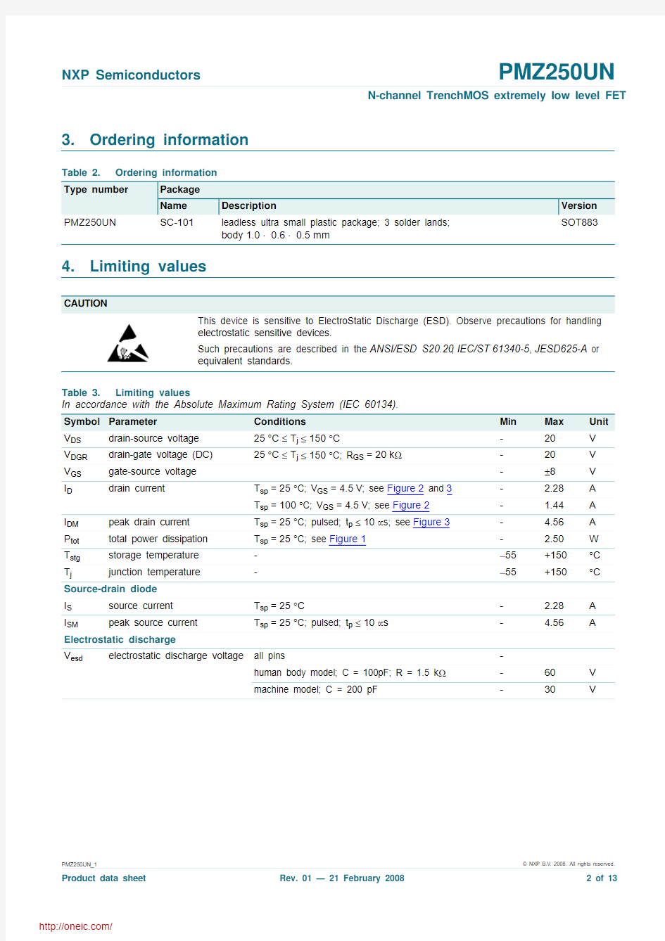
2.Pinning information
PMZ250UN
N-channel TrenchMOS extremely low level FET
Rev. 01 — 21 February 2008
Product data sheet
BOTTOM VIEW
I Pro?le 55 % lower than SOT23I Footprint 90 % smaller than SOT23I Lower on-state resistance I Low threshold voltage I Leadless package
I Fast switching
I Driver circuits
I Load switching in portable appliances
I DC-to-DC converters
I V DS ≤20V
I I D ≤2.28A I R DSon ≤300m ?
I P tot ≤2.50W
Table 1.Pinning
Pin Description Simpli?ed outline Symbol
1gate (G)SOT883 (SC-101)
2source (S)
3
drain (D)
3
1
2
Transparent top view
S
D
G
mbb076
3.Ordering information
4.Limiting values
Table 2.
Ordering information
Type number
Package Name
Description
Version PMZ250UN
SC-101
leadless ultra small plastic package; 3 solder lands;body 1.0×0.6×0.5mm
SOT883
CAUTION
This device is sensitive to ElectroStatic Discharge (ESD). Observe precautions for handling electrostatic sensitive devices.
Such precautions are described in the ANSI/ESD S20.20,IEC/ST 61340-5,JESD625-A or equivalent standards.
Table 3.Limiting values
In accordance with the Absolute Maximum Rating System (IEC 60134).Symbol Parameter Conditions Min Max Unit V DS drain-source voltage 25°C ≤T j ≤150°C
-20V V DGR drain-gate voltage (DC)25°C ≤T j ≤150°C; R GS =20k ?
-20V V GS gate-source voltage -±8V I D drain current T sp =25°C; V GS =4.5V; see Figure 2 and 3- 2.28A T sp =100°C; V GS =4.5V; see Figure 2- 1.44A I DM peak drain current T sp =25°C; pulsed; t p ≤10μs; see Figure 3- 4.56A P tot total power dissipation T sp =25°C; see Figure 1- 2.50W T stg storage temperature -?55+150°C T j junction temperature -?55+150°C Source-drain diode
I S source current T sp =25°C
- 2.28A I SM peak source current
T sp =25°C; pulsed; t p ≤10μs - 4.56
A
Electrostatic discharge
V esd
electrostatic discharge voltage
all pins
-human body model; C = 100pF; R = 1.5 k ?-60V machine model; C = 200 pF -30
V
Fig 1.Normalized total power dissipation as a
function of solder point temperature
Fig 2.Normalized continuous drain current as a
function of solder point temperature
T sp =25°C; I DM is single pulse
Fig 3.Safe operating area; continuous and peak drain currents as a function of drain-source voltage
T sp (°C)
0200
150
50100003aac031
4080
120P der (%)
T sp (°C)
0200
150
50100003aac033
40
80
120I der ( %)
P der P tot
P tot 25°C ()
-----------------------100%
×=I der I D
I D 25°C ()
--------------------100%
×=003aac202
1
10?1
10
102I D (A)10?2
V DS (V)
10?1
102
10
1Limit R DSon = V DS / I D
DC
t p = 10 μs 100 μs
100 ms
1 ms 10 ms
5.Thermal characteristics
[1]
Mounted on a printed-circuit board; vertical in still air.
Table 4.Thermal characteristics
Symbol Parameter
Conditions Min Typ Max Unit R th(j-sp)thermal resistance from junction to solder point see Figure 4--50K/W R th(j-a)
thermal resistance from junction to ambient
minimum footprint
[1]
-
670
-
K/W
Fig 4.Transient thermal impedance from junction to solder point as a function of pulse duration
003aab831
1
10
102
10-4
10-310-210-1
1
10
t p (s)
Z th(j-sp) (K/W)
single pulse
δ = 0.5
0.2
0.10.050.02
t p
T
P
t
t p T
δ =
6.Characteristics
Table 5.Characteristics
T j=25°C unless otherwise speci?ed.
Symbol Parameter Conditions Min Typ Max Unit Static characteristics
V(BR)DSS drain-source breakdown
voltage I D=10μA; V GS=0V
T j=25°C20--V T j=?55°C18--V
V GS(th)gate-source threshold voltage I D=0.25mA;V DS=V GS;see Figure9and10
T j=25°C0.450.70.95V
T j=150°C0.25--V
T j=?55°C-- 1.15V I DSS drain leakage current V DS=20V; V GS=0V
T j=25°C--1μA
T j=150°C--100μA I GSS gate leakage current V GS=±8V; V DS=0V-10100nA
R DSon drain-source on-state
resistance V GS=4.5V; I D=0.2A; see Figure6 and8
T j=25°C-250300m?T j=150°C-400480m?V GS=2.5V; I D=0.1A; see Figure6 and8-320400m?V GS=1.8V; I D=0.075A; see Figure6 and8-420600m?
Dynamic characteristics
Q G(tot)total gate charge I D=1A; V DS=10V; V GS=4.5V; see
Figure11 and12-0.89-nC
Q GS gate-source charge-0.13-nC Q GD gate-drain charge-0.18-nC
C iss input capacitance V GS=0V; V DS=20V; f=1MHz; see
Figure14-45-pF
C oss output capacitance-11-pF C rss reverse transfer capacitance-7-pF t d(on)turn-on delay time V DS=10V; R L=10?; V GS=4.5V; R G=6?- 4.5-ns t r rise time-10-ns t d(off)turn-off delay time-18.5-ns t f fall time-5-ns Source-drain diode
V SD source-drain voltage I S=0.3A; V GS=0V; see Figure13-0.80 1.2V
T j =25°C T j =25°C
Fig 5.Output characteristics: drain current as a
function of drain-source voltage; typical values
Fig 6.Drain-source on-state resistance as a function
of drain current; typical values
T j =25°C and 150°C; V DS >I D ×R DSon
Fig 7.Transfer characteristics: drain current as a
function of gate-source voltage; typical values
Fig 8.Normalized drain-source on-state resistance
factor as a function of junction temperature
V DS (V)
02
1.5
0.5103an02
1
1.5
0.5
2
2.5I D (A)
4.5 2.5
32
1.8
V GS (V) = 1.5
I D (A)
0 2.5
2
1 1.50.503an03
0.4
0.6
0.2
0.8
1R DSon (?)
V GS (V) = 1.8
2
2.5
4.5
3V GS (V)
04
3
1203an04
1
1.5
0.5
2
2.5I D (A)
25 °C
T j = 150 °C
T j (°C)
?60
180
120
060003aac024
1.0
0.5
1.5
2.0a 0a R DSon
R DSon 25°C ()
-----------------------------=
I D =0.25mA; V DS =V GS T j =25°C; V DS =5V
Fig 9.Gate-source threshold voltage as a function of
junction temperature
Fig 10.Sub-threshold drain current as a function of
gate-source voltage
I D =1A; V DS =10V
Fig 11.Gate-source voltage as a function of gate
charge; typical values
Fig 12.Gate charge waveform de?nitions
T j (°C)
?60
180
120
06003aj65
0.6
0.3
0.9
1.2V GS(th)(V)
0max
min
typ
03am43
V GS (V)
0 1.2
0.8
0.410?4
10?5
10?3I D (A)10?6
min typ max
Q G (nC)
10.80.4
0.6
0.2
03an07
2
3
1
4
5V GS (V)
I D = 1 A T j = 25 °C V DS = 10 V
003aaa508
V GS
V GS(th)
Q GS1
Q GS2
Q GD V DS
Q G(tot)
I D
Q GS
V GS(pl)
T j =25°C and 150°C; V GS =0V V GS =0V; f =1MHz
Fig 13.Source current as a function of source-drain
voltage; typical values
Fig 14.Input,output and reverse transfer capacitances
as a function of drain-source voltage; typical values
V SD (V)
010.80.40.6
0.203an97
0.4
0.6
0.2
0.8
1I S (A)0
150 °C
T j = 25 °C
V GS = 0 V
03an06
V DS (V)
10?1
102
10
110
102
C (pF)
1C iss
C oss C rss
7.Package outline
Fig 15.Package outline SOT833 (SC-101)
UNIT A 1max.A (1)b b 1e 1e L L 1 REFERENCES
OUTLINE VERSION EUROPEAN PROJECTION
ISSUE DATE IEC
JEDEC
JEITA mm
0.500.46
0.200.12
0.550.47
0.03
0.620.55
0.35
0.65
DIMENSIONS (mm are the original dimensions)Note
1. Including plating thickness
0.300.22
0.300.22
SOT883
SC-101
03-02-0503-04-03
D E 1.020.95
L
E
23
1
b b 1
A 1
A D
L 1
00.5 1 mm
scale
Leadless ultra small plastic package; 3 solder lands; body 1.0 x 0.6 x 0.5 mm
SOT883
e
e 1
8.Soldering
Dimensions in mm
Fig 16.Re?ow soldering footprint for SOT883
mbl873
1.30
0.30
R = 0.05 (12×)
R = 0.05 (12×)
0.600.700.80
solder lands solder resist occupied area solder paste
0.900.30(2×)0.35(2×)
0.20
0.40(2×)0.50(2×)
0.25(2×)
0.300.400.50
分销商库存信息: NXP
PMZ250UN,315