Features Array?Single 2.5V - 3.6V or 2.7V - 3.6V Supply
?RapidS Serial Interface: 66 MHz Maximum Clock Frequency
–SPI Compatible Modes 0 and 3
?User Configurable Page Size
–512 Bytes per Page
–528 Bytes per Page
–Page Size Can Be Factory Pre-configured for 512 Bytes
?Page Program Operation
–Intelligent Programming Operation
–8,192 Pages (512/528 Bytes/Page) Main Memory
?Flexible Erase Options
–Page Erase (512 Bytes)
–Block Erase (4 Kbytes)
–Sector Erase (64 Kbytes)
–Chip Erase (32 Mbits)
?Two SRAM Data Buffers (512/528 Bytes)
–Allows Receiving of Data while Reprogramming the Flash Array
?Continuous Read Capability through Entire Array
–Ideal for Code Shadowing Applications
?Low-power Dissipation
–7 mA Active Read Current Typical
–25 μA Standby Current Typical
–15 μA Deep Power Down Typical
?Hardware and Software Data Protection Features
–Individual Sector
?Sector Lockdown for Secure Code and Data Storage
–Individual Sector
?Security: 128-byte Security Register
–64-byte User Programmable Space
–Unique 64-byte Device Identifier
?JEDEC Standard Manufacturer and Device ID Read
?100,000 Program/Erase Cycles Per Page Minimum
?Data Retention – 20 Years
?Industrial Temperature Range
?Green (Pb/Halide-free/RoHS Compliant) Packaging Options
1.Description
The AT45DB321D is a 2.5-volt or 2.7-volt, serial-interface sequential access Flash memory ideally suited for a wide variety of digital voice-, image-, program code- and data-storage applications. The AT45DB321D supports RapidS serial interface for applications requiring very high speed operations. RapidS serial interface is SPI com-patible for frequencies up to 66 MHz. Its 34,603,008 bits of memory are organized as 8,192 pages of 512 bytes or 528 bytes each. In addition to the main memory, the AT45DB321D also contains two SRAM buffers of 512/528 bytes each. The buffers allow the receiving of data while a page in the main Memory is being reprogrammed, as well as writing a continuous data stream. EEPROM emulation (bit or byte alterabil-ity) is easily handled with a self-contained three step read-modify-write operation. Unlike conventional Flash memories that are accessed randomly with multiple
address lines and a parallel interface, the DataFlash uses a RapidS serial interface to
2
3597O–DFLASH–10/09
AT45DB321D
sequentially access its data. The simple sequential access dramatically reduces active pin count, facilitates hardware layout, increases system reliability, minimizes switching noise, and reduces package size. The device is optimized for use in many commercial and industrial appli-cations where high-density, low-pin count, low-voltage and low-power are essential.
To allow for simple in-system reprogrammability, the AT45DB321D does not require high input voltages for programming. The device operates from a single power supply, 2.7V to 3.6V, for both the program and read operations. The AT45DB321D is enabled through the chip select pin (CS) and accessed via a three-wire interface consisting of the Serial Input (SI), Serial Output (SO), and the Serial Clock (SCK).
All programming and erase cycles are self-timed.
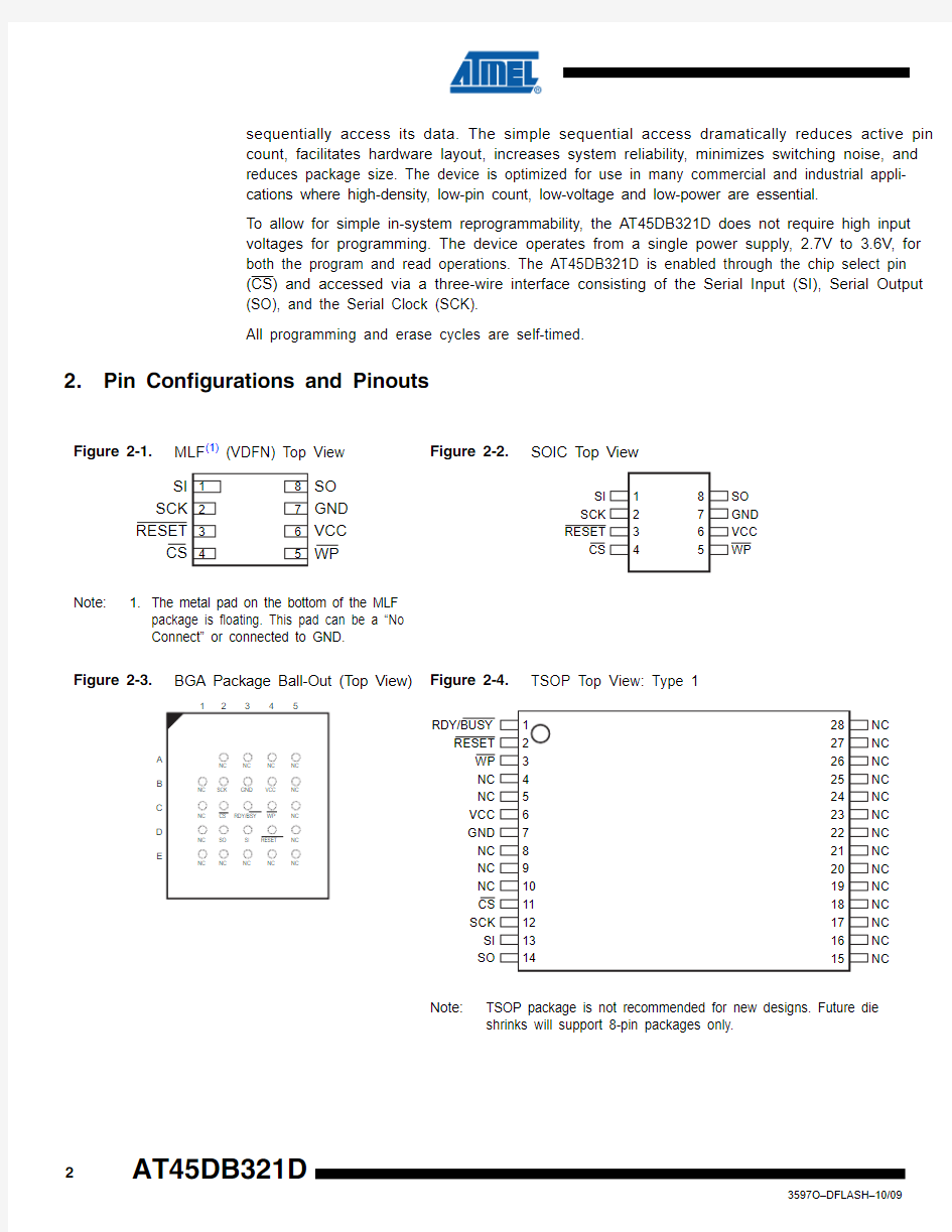
2.Pin Configurations and Pinouts
Figure 2-1.
MLF (1) (VDFN) Top View
Note:
1.The metal pad on the bottom of the MLF
package is floating. This pad can be a “No Connect” or connected to GND.
Figure 2-2.SOIC Top View
Figure 2-3.BGA Package Ball-Out (Top View)
Figure 2-4.
TSOP Top View: Type 1
Note:
TSOP package is not recommended for new designs. Future die shrinks will support 8-pin packages only.
3
3597O–DFLASH–10/09
AT45DB321D
Table 2-1.
Pin Configurations
Symbol
Name and Function
Asserted State
Type
CS Chip Select: Asserting the CS pin selects the device. When the CS pin is deasserted, the device will be deselected and normally be placed in the standby mode (not Deep Power-Down mode), and the output pin (SO) will be in a high-impedance state. When the device is deselected, data will not be accepted on the input pin (SI).
A high-to-low transition on the CS pin is required to start an operation, and a low-to-high
transition is required to end an operation. When ending an internally self-timed operation such as a program or erase cycle, the device will not enter the standby mode until the completion of the operation.
Low Input
SCK Serial Clock: This pin is used to provide a clock to the device and is used to control the flow of data to and from the device. Command, address, and input data present on the SI pin is always latched on the rising edge of SCK, while output data on the SO pin is always clocked out on the falling edge of SCK.
–Input
SI Serial Input: The SI pin is used to shift data into the device. The SI pin is used for all data input including command and address sequences. Data on the SI pin is always latched on the rising edge of SCK.
–Input
SO Serial Output: The SO pin is used to shift data out from the device. Data on the SO pin is always clocked out on the falling edge of SCK.
–Output
WP Write Protect: When the WP pin is asserted, all sectors specified for protection by the Sector Protection Register will be protected against program and erase operations regardless of whether the Enable Sector Protection command has been issued or not. The WP pin functions
independently of the software controlled protection method. After the WP pin goes low, the content of the Sector Protection Register cannot be modified.
If a program or erase command is issued to the device while the WP pin is asserted, the device will simply ignore the command and perform no operation. The device will return to the idle state once the CS pin has been deasserted. The Enable Sector Protection command and Sector Lockdown command, however, will be recognized by the device when the WP pin is asserted.The WP pin is internally pulled-high and may be left floating if hardware controlled protection will not be used. However, it is recommended that the WP pin also be externally connected to V CC whenever possible.
Low Input
RESET Reset: A low state on the reset pin (RESET) will terminate the operation in progress and reset the internal state machine to an idle state. The device will remain in the reset condition as long as a low level is present on the RESET pin. Normal operation can resume once the RESET pin is brought back to a high level.
The device incorporates an internal power-on reset circuit, so there are no restrictions on the RESET pin during power-on sequences. If this pin and feature are not utilized it is recommended that the RESET pin be driven high externally.
Low Input
RDY/BUSY Ready/Busy: This open drain output pin will be driven low when the device is busy in an
internally self-timed operation. This pin, which is normally in a high state (through an external pull-up resistor), will be pulled low during programming/erase operations, compare operations, and page-to-buffer transfers.
The busy status indicates that the Flash memory array and one of the buffers cannot be accessed; read and write operations to the other buffer can still be performed.
–Output
V CC Device Power Supply: The V CC pin is used to supply the source voltage to the device.
Operations at invalid V CC voltages may produce spurious results and should not be attempted.–Power GND
Ground: The ground reference for the power supply. GND should be connected to the system ground.
–
Ground
4
3597O–DFLASH–10/09
AT45DB321D
3.Block Diagram
4.Memory Array
To provide optimal flexibility, the memory array of the AT45DB321D is divided into three levels of granularity comprising of sectors, blocks, and pages. The “Memory Architecture Diagram” illustrates the breakdown of each level and details the number of pages per sector and block. All program operations to the DataFlash occur on a page by page basis. The erase operations can be performed at the chip, sector, block or page level.Figure 4-1.
Memory Architecture Diagram
5
3597O–DFLASH–10/09
AT45DB321D
5.Device Operation
The device operation is controlled by instructions from the host processor. The list of instructions and their associated opcodes are contained in Table 15-1 on page 28 through Table 15-7 on page 31. A valid instruction starts with the falling edge of CS followed by the appropriate 8-bit gling the SCK pin controls the loading of the opcode and the desired buffer or main memory address location through the SI (serial input) pin. All instructions, addresses, and data are trans-ferred with the most significant bit (MSB) first.
Buffer addressing for the DataFlash standard page size (528 bytes) is referenced in the datasheet using the terminology BFA9 - BFA0 to denote the 10 address bits required to desig-nate a byte address within a buffer. Main memory addressing is referenced using the terminology PA12 - PA0 and BA9 - BA0, where PA12 - PA0 denotes the 13 address bits required to designate a page address and BA9 - BA0 denotes the 10 address bits required to designate a byte address within the page.
For “Power of 2” binary page size (512 bytes) the Buffer addressing is referenced in the datasheet using the conventional terminology BFA8 - BFA0 to denote the 9 address bits required to designate a byte address within a buffer. Main memory addressing is referenced using the terminology A21 - A0, where A21 - A9 denotes the 13 address bits required to desig-nate a page address and A8 - A0 denotes the 9 address bits required to designate a byte address within a page.
6.Read Commands
By specifying the appropriate opcode, data can be read from the main memory or from either one of the two SRAM data buffers. The DataFlash supports RapidS protocols for Mode 0 and Mode 3. Please refer to the “Detailed Bit-level Read Timing” diagrams in this datasheet for details on the clock cycle sequences for each mode.
6.1Continuous Array Read (Legacy Command: E8H): Up to 66 MHz
By supplying an initial starting address for the main memory array, the Continuous Array Read command can be utilized to sequentially read a continuous stream of data from the device by simply providing a clock signal; no additional addressing information or control signals need to be provided. The DataFlash incorporates an internal address counter that will automatically increment on every clock cycle, allowing one continuous read operation without the need of additional address sequences. To perform a continuous read from the DataFlash standard page size (528 bytes), an opcode of E8H must be clocked into the device followed by three address bytes (which comprise the 24-bit page and byte address sequence) and 4 don’t care bytes. The first 13 bits (PA12-PA0) of the 23-bit address sequence specify which page of the main mem-ory array to read, and the last 10 bits (BA9-BA0) of the 23-bit address sequence specify the starting byte address within the page. To perform a continuous read from the binary page size (512 bytes), the opcode (E8H) must be clocked into the device followed by three address bytes and 4 don’t care bytes. The first 13 bits (A21 - A9) of the 22-bits sequence specify which page of the main memory array to read, and the last 9 bits (A8 - A0) of the 22-bits address sequence specify the starting byte address within the page. The don’t care bytes that follow the address bytes are needed to initialize the read operation. Following the don’t care bytes, additional clock pulses on the SCK pin will result in data being output on the SO (serial output) pin.
The CS pin must remain low during the loading of the opcode, the address bytes, the don’t care bytes, and the reading of data. When the end of a page in main memory is reached during a
6
3597O–DFLASH–10/09
AT45DB321D
Continuous Array Read, the device will continue reading at the beginning of the next page with no delays incurred during the page boundary crossover (the crossover from the end of one page to the beginning of the next page). When the last bit in the main memory array has been read,the device will continue reading back at the beginning of the first page of memory. As with cross-ing over page boundaries, no delays will be incurred when wrapping around from the end of the array to the beginning of the array.
pin (SO). The maximum SCK frequency allowable for the Continuous Array Read is defined by the f CAR1 specification. The Continuous Array Read bypasses both data buffers and leaves the contents of the buffers unchanged.
6.2Continuous Array Read (High Frequency Mode: 0BH): Up to 66 MHz
This command can be used with the serial interface to read the main memory array sequentially in high speed mode for any clock frequency up to the maximum specified by f CAR1. To perform a opcode 0BH must be clocked into the device followed by three address bytes and a dummy byte. The first 13 bits (PA12 - PA0) of the 23-bit address sequence specify which page of the main memory array to read, and the last 10 bits (BA9 - BA0) of the 23-bit address sequence specify the starting byte address within the page. To perform a continuous read with the page size set to 512 bytes, the opcode, 0BH, must be clocked into the device followed by three address bytes (A21 - A0) and a dummy byte. Following the dummy byte, additional clock pulses on the SCK pin will result in data being output on the SO (serial output) pin.
The CS pin must remain low during the loading of the opcode, the address bytes, and the read-ing of data. When the end of a page in the main memory is reached during a Continuous Array Read, the device will continue reading at the beginning of the next page with no delays incurred during the page boundary crossover (the crossover from the end of one page to the beginning of the next page). When the last bit in the main memory array has been read, the device will con-tinue reading back at the beginning of the first page of memory. As with crossing over page boundaries, no delays will be incurred when wrapping around from the end of the array to the beginning of the array. A low-to-high transition on the CS pin will terminate the read operation and tri-state the output pin (SO). The maximum SCK frequency allowable for the Continuous Array Read is defined by the f CAR1 specification. The Continuous Array Read bypasses both data buffers and leaves the contents of the buffers unchanged.
6.3Continuous Array Read (Low Frequency Mode: 03H): Up to 33 MHz
This command can be used with the serial interface to read the main memory array sequentially without a dummy byte up to maximum frequencies specified by f CAR2. To perform a continuous read array with the page size set to 528 bytes, the CS must first be asserted then an opcode,03H, must be clocked into the device followed by three address bytes (which comprise the 24-bit page and byte address sequence). The first 13 bits (PA12 - PA0) of the 23-bit address sequence specify which page of the main memory array to read, and the last 10 bits (BA9 - BA0) of the 23-bit address sequence specify the starting byte address within the page. To perform a contin-uous read with the page size set to 512 bytes, the opcode, 03H, must be clocked into the device followed by three address bytes (A21 - A0). Following the address bytes, additional clock pulses on the SCK pin will result in data being output on the SO (serial output) pin.
The CS pin must remain low during the loading of the opcode, the address bytes, and the read-ing of data. When the end of a page in the main memory is reached during a Continuous Array Read, the device will continue reading at the beginning of the next page with no delays incurred
7
3597O–DFLASH–10/09
AT45DB321D
during the page boundary crossover (the crossover from the end of one page to the beginning of the next page). When the last bit in the main memory array has been read, the device will con-tinue reading back at the beginning of the first page of memory. As with crossing over page boundaries, no delays will be incurred when wrapping around from the end of the array to the beginning of the array. A low-to-high transition on the CS pin will terminate the read operation and tri-state the output pin (SO). The Continuous Array Read bypasses both data buffers and leaves the contents of the buffers unchanged.
6.4Main Memory Page Read
A main memory page read allows the user to read data directly from any one of the 8,192 pages in the main memory, bypassing both of the data buffers and leaving the contents of the buffers unchanged. To start a page read from the DataFlash standard page size (528 bytes), an opcode of D2H must be clocked into the device followed by three address bytes (which comprise the 24-bit page and byte address sequence) and 4 don’t care bytes. The first 13 bits (PA12-PA0) of the 23-bit address sequence specify the page in main memory to be read, and the last 10 bits (BA9-BA0) of the 23-bit address sequence specify the starting byte address within that page.To start a page read from the binary page size (512 bytes), the opcode D2H must be clocked into the device followed by three address bytes and 4 don’t care bytes. The first 13 bits (A21 - A9) of the 22-bits sequence specify which page of the main memory array to read, and the last 9 bits (A8 - A0) of the 22-bits address sequence specify the starting byte address within the page. The don’t care bytes that follow the address bytes are sent to initialize the read opera-tion. Following the don’t care bytes, additional pulses on SCK result in data being output on the address bytes, the don’t care bytes, and the reading of data. When the end of a page in main memory is reached, the device will continue reading back at the beginning of the same page. A low-to-high transition on the CS pin will terminate the read operation and tri-state the output pin (SO). The maximum SCK frequency allowable for the Main Memory Page Read is defined by the f SCK specification. The Main Memory Page Read bypasses both data buffers and leaves the contents of the buffers unchanged.
6.5Buffer Read
The SRAM data buffers can be accessed independently from the main memory array, and utiliz-ing the Buffer Read Command allows data to be sequentially read directly from the buffers. Four opcodes, D4H or D1H for buffer 1 and D6H or D3H for buffer 2 can be used for the Buffer Read Command. The use of each opcode depends on the maximum SCK frequency that will be used to read data from the buffer. The D4H and D6H opcode can be used at any SCK frequency up to the maximum specified by f CAR1. The D1H and D3H opcode can be used for lower frequency read operations up to the maximum specified by f CAR2.
To perform a buffer read from the DataFlash standard buffer (528 bytes), the opcode must be clocked into the device followed by three address bytes comprised of 14 don’t care bits and 10buffer address bits (BFA9-BFA0). To perform a buffer read from the binary buffer (512bytes), the opcode must be clocked into the device followed by three address bytes com-prised of 15 don’t care bits and 9 buffer address bits (BFA8 - BFA0). Following the address bytes, one don’t care byte must be clocked in to initialize the read operation. The CS pin must remain low during the loading of the opcode, the address bytes, the don’t care byte, and the reading of data. When the end of a buffer is reached, the device will continue reading back at the and tri-state the output pin (SO).
8
3597O–DFLASH–10/09
AT45DB321D
7.Program and Erase Commands
7.1
Buffer Write
Data can be clocked in from the input pin (SI) into either buffer 1 or buffer 2. To load data into the DataFlash standard buffer (528 bytes), a 1-byte opcode, 84H for buffer 1 or 87H for buffer 2,must be clocked into the device, followed by three address bytes comprised of 14 don’t care bits and 10 buffer address bits (BFA9-BFA0). The 10 buffer address bits specify the first byte in the buffer to be written. To load data into the binary buffers (512 bytes each), a 1-byte opcode 84H for buffer 1 or 87H for buffer 2, must be clocked into the device, followed by three address bytes comprised of 15 don’t care bits and 9 buffer address bits (BFA8 - BFA0). The 9 buffer address bits specify the first byte in the buffer to be written. After the last address byte has been clocked into the device, data can then be clocked in on subsequent clock cycles. If the end of the data buffer is reached, the device will wrap around back to the beginning of the buffer. Data will con-tinue to be loaded into the buffer until a low-to-high transition is detected on the CS pin.
7.2Buffer to Main Memory Page Program with Built-in Erase
Data written into either buffer 1 or buffer 2 can be programmed into the main memory. A 1-byte opcode, 83H for buffer 1 or 86H for buffer 2, must be clocked into the device. For the DataFlash standard page size (528 bytes), the opcode must be followed by three address bytes consist of 1 don’t care bit, 13 page address bits (PA12 - PA0) that specify the page in the main memory to be written and 10 don’t care bits. To perform a buffer to main memory page program with built-in erase for the binary page size (512 bytes), the opcode 83H for buffer 1 or 86H for buffer 2, must be clocked into the device followed by three address bytes consisting of 2 don’t care bits 13-page address bits (A21 - A9) that specify the page in the main memory to be written and 9selected page in main memory (the erased state is a logic 1) and then program the data stored in the buffer into the specified page in main memory. Both the erase and the programming of the page are internally self-timed and should take place in a maximum time of t EP . During this time,7.3Buffer to Main Memory Page Program without Built-in Erase
A previously-erased page within main memory can be programmed with the contents of either buffer 1 or buffer 2. A 1-byte opcode, 88H for buffer 1 or 89H for buffer 2, must be clocked into the device. For the DataFlash standard page size (528 bytes), the opcode must be followed by three address bytes consist of 1 don’t care bit, 13 page address bits (PA12-PA0) that specify the page in the main memory to be written and 10 don’t care bits. To perform a buffer to main memory page program without built-in erase for the binary page size (512 bytes), the opcode 88H for buffer 1 or 89H for buffer 2, must be clocked into the device followed by three address bytes consisting of 2 don’t care bits, 13 page address bits (A21 - A9) that specify the page in the main memory to be written and 9 don’t care bits. When a low-to-high transition occurs on the CS pin, the part will program the data stored in the buffer into the specified page in the main mem-ory. It is necessary that the page in main memory that is being programmed has been previously erased using one of the erase commands (Page Erase or Block Erase). The programming of the page is internally self-timed and should take place in a maximum time of t P . During this time, the
9
3597O–DFLASH–10/09
AT45DB321D
7.4
Page Erase
The Page Erase command can be used to individually erase any page in the main memory array allowing the Buffer to Main Memory Page Program to be utilized at a later time. To perform a page erase in the DataFlash standard page size (528bytes), an opcode of 81H must be loaded into the device, followed by three address bytes comprised of 1 don’t care bit, 13 page address bits (PA12-PA0) that specify the page in the main memory to be erased and 10 don’t care bits.To perform a page erase in the binary page size (512 bytes), the opcode 81H must be loaded into the device, followed by three address bytes consist of 2 don’t care bits, 13 page address bits (A21 - A9) that specify the page in the main memory to be erased and 9 don’t care bits. When a state is a logical 1). The erase operation is internally self-timed and should take place in a maxi-mum time of t PE part is busy.
7.5Block Erase
A block of eight pages can be erased at one time. This command is useful when large amounts of data has to be written into the device. This will avoid using multiple Page Erase Commands.To perform a block erase for the DataFlash standard page size (528bytes), an opcode of 50H must be loaded into the device, followed by three address bytes comprised of 1 don’t care bit,10page address bits (PA12-PA3) and 13 don’t care bits. The 10 page address bits are used to specify which block of eight pages is to be erased. To perform a block erase for the binary page size (512 bytes), the opcode 50H must be loaded into the device, followed by three address bytes consisting of 2 don’t care bits, 10 page address bits (A21 - A12) and 12 don’t care bits.The 10 page address bits are used to specify which block of eight pages is to be erased. When a low-to-high transition occurs on the CS pin, the part will erase the selected block of eight pages. The erase operation is internally self-timed and should take place in a maximum time of t BE . During this time, the status register and the RDY/BUSY pin will indicate that the part is busy.
Table 7-1.
Block Erase Addressing
PA12/A21PA11/A20PA10/A19PA9/A18PA8/A17PA7/A16PA6/A15PA5/A14PA4/A13PA3/A12PA2/A11PA1/A10PA0/A9Block 0000000000X X X 00000000001X X X 10000000010X X X 20000000011X X X 3??????????????????????????????????????????1111111100X X X 10201111111101X X X 10211111111110X X X 10221
1
1
1
1
1
1
1
1
1
X
X
X
1023
10
3597O–DFLASH–10/09
AT45DB321D
7.6Sector Erase
The Sector Erase command can be used to individually erase any sector in the main memory.There are 64 sectors and only one sector can be erased at one time. To perform sector 0a or sector 0b erase for the DataFlash standard page size (528 bytes), an opcode of 7CH must be loaded into the device, followed by three address bytes comprised of 1 don’t care bit, 10 page address bits (PA12 - PA3) and 13 don’t care bits. To perform a sector 1-63 erase, the opcode 7CH must be loaded into the device, followed by three address bytes comprised of 1 don’t care bit, 6 page address bits (PA12 - PA7) and 17 don’t care bits. To perform sector 0a or sector 0b erase for the binary page size (512 bytes), an opcode of 7CH must be loaded into the device,followed by three address bytes comprised of 2 don’t care bit and 10 page address bits (A21 - A12) and 12 don’t care bits. To perform a sector 1-63 erase, the opcode 7CH must be loaded into the device, followed by three address bytes comprised of 2 don’t care bits and 6page address bits (A21 - A16) and 16 don’t care bits. The page address bits are used to spec-ify any valid address location within the sector which is to be erased. When a low-to-high transition occurs on the CS pin, the part will erase the selected sector. The erase operation is internally self-timed and should take place in a maximum time of t SE . During this time, the status register and the RDY/BUSY pin will indicate that the part is busy.
7.7
Chip Erase (1)
The entire main memory can be erased at one time by using the Chip Erase command.To execute the Chip Erase command, a 4-byte command sequence C7H, 94H, 80H and 9AH must be clocked into the device. Since the entire memory array is to be erased, no address bytes need to be clocked into the device, and any data clocked in after the opcode will be ignored. After the last bit of the opcode sequence has been clocked in, the CS pin can be deas-serted to start the erase process. The erase operation is internally self-timed and should take place in a time of t CE . During this time, the Status Register will indicate that the device is busy.The Chip Erase command will not affect sectors that are protected or locked down; the contents of those sectors will remain unchanged. Only those sectors that are not protected or locked down will be erased.
Note:
1.Refer to the errata regarding Chip Erase on page 56.
Table 7-2.
Sector Erase Addressing
PA12/A21PA11/A20PA10/A19PA9/A18PA8/A17PA7/A16PA6/A15PA5/A14PA4/A13PA3/A12PA2/A11PA1/A10PA0/A9Sector 0000000000X X X 0a 0000000001X X X 0b 000001X X X X X X X 1000010X X X X X X X 2??????????????????????????????????????????111100X X X X X X X 60111101X X X X X X X 61111110X X X X X X X 621
1
1
1
1
1
X
X
X
X
X
X
X
63
11
3597O–DFLASH–10/09
AT45DB321D
the internal erase cycle completes.
Figure 7-1.Chip Erase
Note: 1.Refer to the errata regarding Chip Erase on page 56.
7.8Main Memory Page Program Through Buffer
This operation is a combination of the Buffer Write and Buffer to Main Memory Page Program with Built-in Erase operations. Data is first clocked into buffer 1 or buffer 2 from the input pin (SI)and then programmed into a specified page in the main memory. To perform a main memory page program through buffer for the DataFlash standard page size (528 bytes), a 1-byte opcode,82H for buffer 1 or 85H for buffer 2, must first be clocked into the device, followed by three address bytes. The address bytes are comprised of 1 don’t care bit, 13 page address bits,(PA12-PA0) that select the page in the main memory where data is to be written, and 10 buffer address bits (BFA9-BFA0) that select the first byte in the buffer to be written. To perform a main memory page program through buffer for the binary page size (512 bytes), the opcode 82H for buffer 1 or 85H for buffer 2, must be clocked into the device followed by three address bytes consisting of 2 don’t care bits, 13 page address bits (A21 - A9) that specify the page in the main memory to be written, and 9 buffer address bits (BFA8 - BFA0) that selects the first byte in the buffer to be written. After all address bytes are clocked in, the part will take data from the input pins and store it in the specified data buffer. If the end of the buffer is reached, the device will wrap around back to the beginning of the buffer. When there is a low-to-high transition on the CS pin, the part will first erase the selected page in main memory to all 1s and then program the data stored in the buffer into that memory page. Both the erase and the programming of the page are internally self-timed and should take place in a maximum time of t EP . During this time,the status register and the RDY/BUSY pin will indicate that the part is busy.
8.Sector Protection
Two protection methods, hardware and software controlled, are provided for protection against inadvertent or erroneous program and erase cycles. The software controlled method relies on the use of software commands to enable and disable sector protection while the hardware con-trolled method employs the use of the Write Protect (WP) pin. The selection of which sectors that are to be protected or unprotected against program and erase operations is specified in the nonvolatile Sector Protection Register. The status of whether or not sector protection has been enabled or disabled by either the software or the hardware controlled methods can be deter-mined by checking the Status Register.
Command Byte 1Byte 2Byte 3Byte 4Chip Erase
C7H
94H
80H
9AH
12
3597O–DFLASH–10/09
AT45DB321D
8.1
Software Sector Protection
8.1.1
Enable Sector Protection Command
Sectors specified for protection in the Sector Protection Register can be protected from program and erase operations by issuing the Enable Sector Protection command. To enable the sector protection using the software controlled method, the CS pin must first be asserted as it would be sequence must be clocked in via the input pin (SI). After the last bit of the command sequence enabled.
Figure 8-1.Enable Sector Protection
8.1.2
Disable Sector Protection Command
asserted as it would be with any other command. Once the CS pin has been asserted, the appropriate 4-byte sequence for the Disable Sector Protection command must be clocked in via the input pin (SI). After the last bit of the command sequence has been clocked in, the CS pin deasserted state; otherwise, the Disable Sector Protection command will be ignored.
Figure 8-2.Disable Sector Protection
8.1.3
Various Aspects About Software Controlled Protection
controlled by a host processor. In such instances, the WP pin may be left floating (the WP pin is internally pulled high) and sector protection can be controlled using the Enable Sector Protection and Disable Sector Protection commands.
If the device is power cycled, then the software controlled protection will be disabled. Once the device is powered up, the Enable Sector Protection command should be reissued if sector pro-tection is desired and if the WP pin is not used.
Command
Byte 1Byte 2Byte 3Byte 4Enable Sector Protection
3DH
2AH
7FH
A9H
Command
Byte 1Byte 2Byte 3Byte 4Disable Sector Protection
3DH
2AH
7FH
9AH
13
3597O–DFLASH–10/09
AT45DB321D
9.Hardware Controlled Protection
Sectors specified for protection in the Sector Protection Register and the Sector Protection Reg-keeping the pin in its asserted state. The Sector Protection Register and any sector specified for modify the Sector Protection Register, the WP pin must be deasserted. If the WP pin is perma-nently connected to GND, then the content of the Sector Protection Register cannot be changed.If the WP pin is deasserted, or permanently connected to V CC , then the content of the Sector Protection Register can be modified.
The WP pin will override the software controlled protection method but only for protecting the sectors. For example, if the sectors were not previously protected by the Enable Sector Protec-tion command, then simply asserting the WP pin would enable the sector protection within the maximum specified t WPE would no longer be enabled (after the maximum specified t WPD time) as long as the Enable Sec-Protection command was issued before or while the WP pin was asserted, then simply deassert-Protection command would need to be issued while the WP pin is deasserted to disable the sec-asserted.
A noise filter is incorporated to help protect against spurious noise that may inadvertently assert or deassert the WP pin.
Enable Sector Protection command, and the Disable Sector Protection command.
Figure 9-1.
Table 9-1.
Time Period WP Pin Enable Sector Protection
Command Disable Sector Protection Command Sector Protection
Status
Sector Protection Register 1High Command Not Issued Previously
–
Issue Command
X
Issue Command
–
Disabled Disabled Enabled Read/Write Read/Write Read/Write 2
Low
X
X
Enabled Read Only 3High
Command Issued During Period 1
or 2–
Issue Command
Not Issued Y et Issue Command
–
Enabled Disabled Enabled
Read/Write Read/Write Read/Write
14
3597O–DFLASH–10/09
AT45DB321D
9.1Sector Protection Register
The nonvolatile Sector Protection Register specifies which sectors are to be protected or unpro-tected with either the software or hardware controlled protection methods. The Sector Protection Register contains 64 bytes of data, of which byte locations 0 through 63 contain values that specify whether sectors 0 through 63 will be protected or unprotected. The Sector Protection Register is user modifiable and must first be erased before it can be reprogrammed. Table 9-3illustrates the format of the Sector Protection Register.:Note:
1.The default value for bytes 0 through 63 when shipped from Atmel is 00H.
x = don’t care.
Table 9-2.
Sector Protection Register
Sector Number
0 (0a, 0b) 1 to 63Protected See Table 9-3
FFH Unprotected
00H
Table 9-3.Sector 0 (0a, 0b)
0a
0b
Bit 3, 2
Data Value (Pages 0-7) (Pages 8-127)
Bit 7, 6
Bit 5, 4
Bit 1, 0
Sectors 0a, 0b Unprotected 0000xx xx 0xH Protect Sector 0a (Pages 0-7)1100xx xx CxH Protect Sector 0b (Pages 8-127)0011xx xx 3xH Protect Sectors 0a (Pages 0-7), 0b (Pages 8-127)(1)11
11
xx
xx
FxH
15
3597O–DFLASH–10/09
AT45DB321D
9.1.1
Erase Sector Protection Register Command
In order to modify and change the values of the Sector Protection Register, it must first be erased using the Erase Sector Protection Register command.
any other command. Once the CS pin has been asserted, the appropriate 4-byte opcode sequence must be clocked into the device via the SI pin. The 4-byte opcode sequence must start with 3DH and be followed by 2AH, 7FH, and CFH. After the last bit of the opcode sequence cycle. The erasing of the Sector Protection Register should take place in a time of t PE , during which time the Status Register will indicate that the device is busy. If the device is powered-down before the completion of the erase cycle, then the contents of the Sector Protection Regis-ter cannot be guaranteed.
The Sector Protection Register can be erased with the sector protection enabled or disabled.Since the erased state (FFH) of each byte in the Sector Protection Register is used to indicate that a sector is specified for protection, leaving the sector protection enabled during the erasing of the register allows the protection scheme to be more effective in the prevention of accidental programming or erasing of the device. If for some reason an erroneous program or erase com-mand is sent to the device immediately after erasing the Sector Protection Register and before the register can be reprogrammed, then the erroneous program or erase command will not be processed because all sectors would be protected.
Figure 9-2.Erase Sector Protection Register
9.1.2
Program Sector Protection Register Command
Once the Sector Protection Register has been erased, it can be reprogrammed using the Pro-gram Sector Protection Register command.
ate 4-byte opcode sequence must be clocked into the device via the SI pin. The 4-byte opcode sequence must start with 3DH and be followed by 2AH, 7FH, and FCH. After the last bit of the opcode sequence has been clocked into the device, the data for the contents of the Sector Pro-tection Register must be clocked in. As described in Section 9.1, the Sector Protection Register contains 64 bytes of data, so 64 bytes must be clocked into the device. The first byte of data cor-responds to sector 0, the second byte corresponds to sector 1, and so on with the last byte of data corresponding to sector 63.
Command
Byte 1Byte 2Byte 3Byte 4Erase Sector Protection Register
3DH
2AH
7FH
CFH
16
3597O–DFLASH–10/09
AT45DB321D
nally self-timed program cycle. The programming of the Sector Protection Register should take place in a time of t P , during which time the Status Register will indicate that the device is busy. If the device is powered-down during the program cycle, then the contents of the Sector Protection Register cannot be guaranteed.
If the proper number of data bytes is not clocked in before the CS pin is deasserted, then the protection status of the sectors corresponding to the bytes not clocked in can not be guaranteed.For example, if only the first two bytes are clocked in instead of the complete 62 bytes, then the protection status of the last 62 sectors cannot be guaranteed. Furthermore, if more than 64bytes of data is clocked into the device, then the data will wrap back around to the beginning of the register. For instance, if 65 bytes of data are clocked in, then the 65th byte will be stored at byte location 0 of the Sector Protection Register.
If a value other than 00H or FFH is clocked into a byte location of the Sector Protection Register,then the protection status of the sector corresponding to that byte location cannot be guaran-teed. For example, if a value of 17H is clocked into byte location 2 of the Sector Protection Register, then the protection status of sector 2 cannot be guaranteed.
The Sector Protection Register can be reprogrammed while the sector protection enabled or dis-abled. Being able to reprogram the Sector Protection Register with the sector protection enabled allows the user to temporarily disable the sector protection to an individual sector rather than dis-abling sector protection completely.
The Program Sector Protection Register command utilizes the internal SRAM buffer 1 for pro-cessing. Therefore, the contents of the buffer 1 will be altered from its previous state when this command is issued.
Figure 9-3.Program Sector Protection Register
Command
Byte 1Byte 2Byte 3Byte 4Program Sector Protection Register
3DH
2AH
7FH
FCH
17
3597O–DFLASH–10/09
AT45DB321D
9.1.3
Read Sector Protection Register Command
been asserted, an opcode of 32H and 3 dummy bytes must be clocked in via the SI pin. After the last bit of the opcode and dummy bytes have been clocked in, any additional clock pulses on the SCK pins will result in data for the content of the Sector Protection Register being output on the SO pin. The first byte corresponds to sector 0 (0a, 0b), the second byte corresponds to sector 1and the last byte (byte 64) corresponds to sector 63. Once the last byte of the Sector Protection Register has been clocked out, any additional clock pulses will result in undefined data being output on the SO pin. The CS must be deasserted to terminate the Read Sector Protection Reg-ister operation and put the output into a high-impedance state.
Note:
xx = Dummy Byte
Figure 9-4.Read Sector Protection Register
9.1.4
Various Aspects About the Sector Protection Register
The Sector Protection Register is subject to a limit of 10,000 erase/program cycles. Users are encouraged to carefully evaluate the number of times the Sector Protection Register will be modified during the course of the applications’ life cycle. If the application requires that the Sec-tor Protection Register be modified more than the specified limit of 10,000 cycles because the application needs to temporarily unprotect individual sectors (sector protection remains enabled while the Sector Protection Register is reprogrammed), then the application will need to limit this practice. Instead, a combination of temporarily unprotecting individual sectors along with dis-abling sector protection completely will need to be implemented by the application to ensure that the limit of 10,000 cycles is not exceeded.
Command
Byte 1Byte 2Byte 3Byte 4Read Sector Protection Register 32H
xxH
xxH
xxH
18
3597O–DFLASH–10/09
AT45DB321D
10.Security Features
10.1
Sector Lockdown
The device incorporates a Sector Lockdown mechanism that allows each individual sector to be permanently locked so that it becomes read only. This is useful for applications that require the ability to permanently protect a number of sectors against malicious attempts at altering program code or security information. Once a sector is locked down, it can never be erased or pro-grammed, and it can never be unlocked.
any other command. Once the CS pin has been asserted, the appropriate 4-byte opcode sequence must be clocked into the device in the correct order. The 4-byte opcode sequence must start with 3DH and be followed by 2AH, 7FH, and 30H. After the last byte of the command sequence has been clocked in, then three address bytes specifying any address within the sec-tor to be locked down must be clocked into the device. After the last address bit has been sequence.
The lockdown sequence should take place in a maximum time of t P , during which time the Status Register will indicate that the device is busy. If the device is powered-down before the comple-tion of the lockdown sequence, then the lockdown status of the sector cannot be guaranteed. In this case, it is recommended that the user read the Sector Lockdown Register to determine the status of the appropriate sector lockdown bits or bytes and reissue the Sector Lockdown com-mand if necessary.
Figure 10-1.Sector Lockdown
Command Byte 1Byte 2Byte 3Byte 4Sector Lockdown
3DH
2AH
7FH
30H
19
3597O–DFLASH–10/09
AT45DB321D
10.1.1
Sector Lockdown Register
Sector Lockdown Register is a nonvolatile register that contains 64 bytes of data, as shown below:
10.1.2
Reading the Sector Lockdown Register
The Sector Lockdown Register can be read to determine which sectors in the memory array are permanently locked down. To read the Sector Lockdown Register, the CS pin must first be clocked into the device via the SI pin. After the last bit of the opcode and dummy bytes have been clocked in, the data for the contents of the Sector Lockdown Register will be clocked out on the SO pin. The first byte corresponds to sector 0 (0a, 0b) the second byte corresponds to sector 1 and the last byte (byte 16) corresponds to sector 15. After the last byte of the Sector Lockdown Register has been read, additional pulses on the SCK pin will simply result in unde-fined data being output on the SO pin.
Deasserting the CS pin will terminate the Read Sector Lockdown Register operation and put the SO pin into a high-impedance state.
Table 10-2 details the values read from the Sector Lockdown Register.Figure 10-2.Read Sector Lockdown Register
Sector Number 0 (0a, 0b) 1 to 63Locked See Below
FFH Unlocked
00H
Table 10-1.Sector 0 (0a, 0b)
0a
0b
Bit 3, 2
Data Value (Pages 0-7) (Pages 8-127)
Bit 7, 6
Bit 5, 4
Bit 1, 0
Sectors 0a, 0b Unlocked 0000000000H Sector 0a Locked (Pages 0-7)11000000C0H Sector 0b Locked (Pages 8-127)0011000030H Sectors 0a, 0b Locked (Pages 0-127)
11
11
00
00
F0H
Table 10-2.
Sector Lockdown Register
Command
Byte 1Byte 2Byte 3Byte 4Read Sector Lockdown Register 35H
xxH
xxH
xxH
Note:
xx = Dummy Byte
20
3597O–DFLASH–10/09
AT45DB321D
10.2Security Register
The device contains a specialized Security Register that can be used for purposes such as unique device serialization or locked key storage. The register is comprised of a total of 128bytes that is divided into two portions. The first 64 bytes (byte locations 0 through 63) of the Security Register are allocated as a one-time user programmable space. Once these 64 bytes have been programmed, they cannot be reprogrammed. The remaining 64 bytes of the register (byte locations 64 through 127) are factory programmed by Atmel and will contain a unique value for each device. The factory programmed data is fixed and cannot be changed.10.2.1
Programming the Security Register
The user programmable portion of the Security Register does not need to be erased before it is programmed.
To program the Security Register, the CS pin must first be asserted and the appropriate 4-byte opcode sequence must be clocked into the device in the correct order. The 4-byte opcode sequence must start with 9BH and be followed by 00H, 00H, and 00H. After the last bit of the opcode sequence has been clocked into the device, the data for the contents of the 64-byte user programmable portion of the Security Register must be clocked in.
After the last data byte has been clocked in, the CS pin must be deasserted to initiate the inter-nally self-timed program cycle. The programming of the Security Register should take place in a time of t P , during which time the Status Register will indicate that the device is busy. If the device is powered-down during the program cycle, then the contents of the 64-byte user programmable portion of the Security Register cannot be guaranteed.
If the full 64 bytes of data is not clocked in before the CS pin is deasserted, then the values of the byte locations not clocked in cannot be guaranteed. For example, if only the first two bytes are clocked in instead of the complete 64 bytes, then the remaining 62 bytes of the user pro-grammable portion of the Security Register cannot be guaranteed. Furthermore, if more than 64bytes of data is clocked into the device, then the data will wrap back around to the beginning of the register. For instance, if 65 bytes of data are clocked in, then the 65th byte will be stored at byte location 0 of the Security Register.
The user programmable portion of the Security Register can only be programmed one time. Therefore, it is not possible to only program the first two bytes of the register and then pro-gram the remaining 62 bytes at a later time.
The Program Security Register command utilizes the internal SRAM buffer 1 for processing.Therefore, the contents of the buffer 1 will be altered from its previous state when this command is issued.
Figure 10-3.Program Security Register
Table 10-3.
Security Register
Security Register Byte Number
1
? ? ?
62
63
64
65
? ? ?
126
127
Data Type
One-time User Programmable
Factory Programmed By Atmel