Data sheet acquired from Harris Semiconductor SCHS208D Features ?Wide Analog-Input-Voltage Range. . . . . . . . . .0V - 10V ?Low “ON” Resistance -V CC = 4.5V. . . . . . . . . . . . . . . . . . . . . . . . . . . . . . . .25?-V CC = 9V . . . . . . . . . . . . . . . . . . . . . . . . . . . . . . . . .15??Fast Switching and Propagation Delay Times ?Low “OFF” Leakage Current ?Wide Operating Temperature Range . . .-55o C to 125o C ?HC Types -2V to 10V Operation -High Noise Immunity: N IL = 30%, N IH = 30% of V CC at V CC = 5V and 10V ?HCT Types
-Direct LSTTL Input Logic Compatibility,
V IL = 0.8V (Max), V IH = 2V (Min)
-CMOS Input Compatibility, I l ≤1μA at V OL , V OH Description
The ’HC4066and CD74HCT4066contain four independent
digitally controlled analog switches that use silicon-gate
CMOS technology to achieve operating speeds similar to
LSTTL with the low power consumption of standard CMOS
integrated circuits.
These switches feature the characteristic linear “ON”
resistance of the metal-gate CD4066B.Each switch is
turned on by a high-level voltage on its control input.Pinout
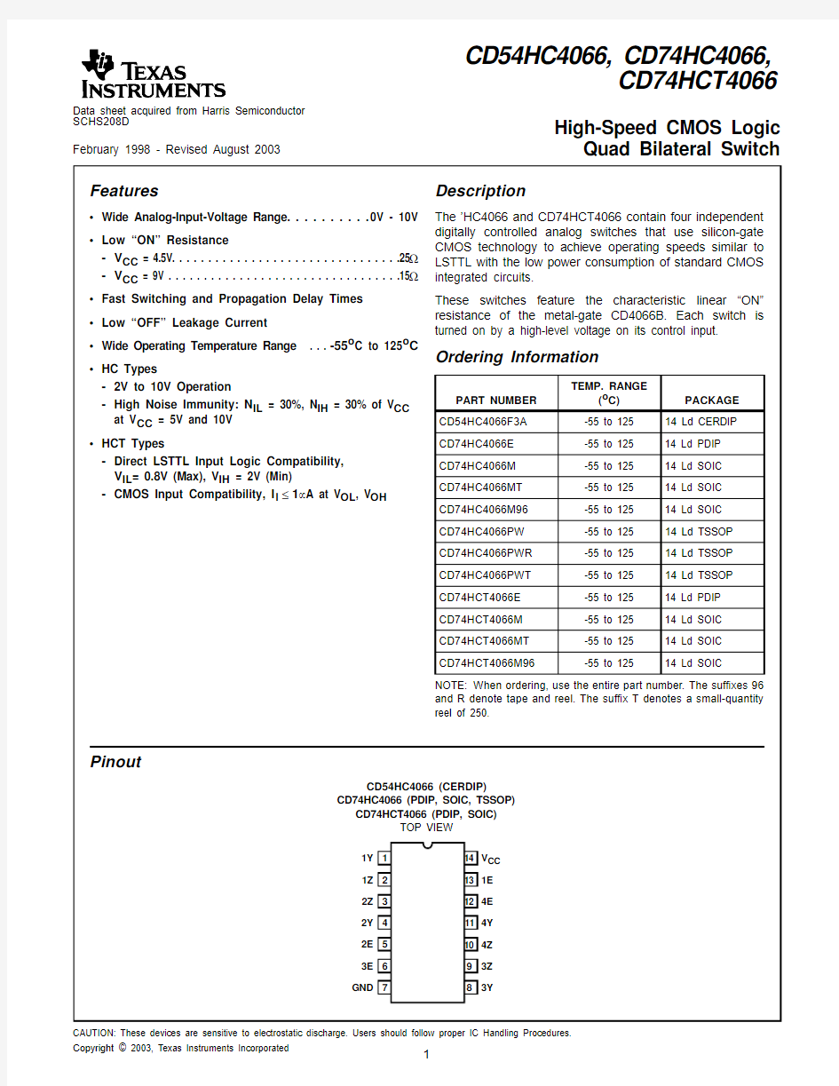
CD54HC4066 (CERDIP)
CD74HC4066 (PDIP, SOIC, TSSOP)
CD74HCT4066 (PDIP, SOIC)
TOP VIEW
Ordering Information PART NUMBER TEMP. RANGE (o C)PACKAGE CD54HC4066F3A -55 to 12514 Ld CERDIP CD74HC4066E -55 to 12514 Ld PDIP CD74HC4066M -55 to 12514 Ld SOIC CD74HC4066MT
-55 to 12514 Ld SOIC CD74HC4066M96
-55 to 12514 Ld SOIC CD74HC4066PW
-55 to 12514 Ld TSSOP CD74HC4066PWR
-55 to 12514 Ld TSSOP CD74HC4066PWT
-55 to 12514 Ld TSSOP CD74HCT4066E
-55 to 12514 Ld PDIP CD74HCT4066M
-55 to 12514 Ld SOIC CD74HCT4066MT
-55 to 12514 Ld SOIC CD74HCT4066M96-55 to 12514 Ld SOIC
NOTE:When ordering,use the entire part number.The suf?xes 96
and R denote tape and reel.The suf?x T denotes a small-quantity
reel of 250.
1Y 1Z 2Z 2Y 2E 3E GND V CC 1E 4E 4Y 4Z 3Z 3Y
1
2
3
4
5
6
7141312111098February 1998 - Revised August 2003CD54HC4066, CD74HC4066,CD74HCT4066
High-Speed CMOS Logic Quad Bilateral Switch
[ /Title (CD74H C4066,CD74H CT4066)
/Subject
(High-
Speed
CMOS
Logic
Quad
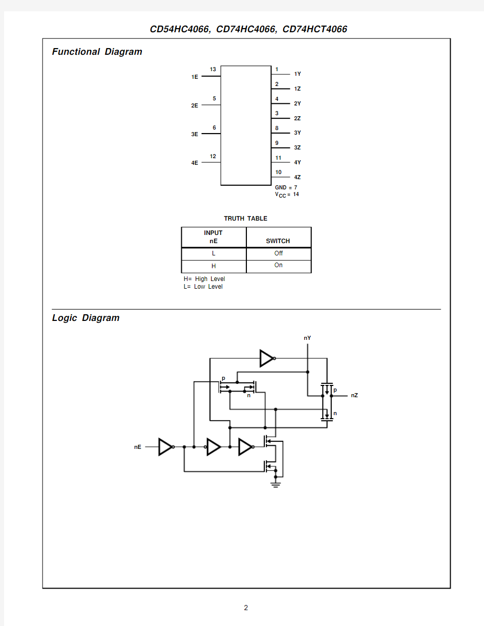
Functional Diagram
Logic Diagram
TRUTH TABLE
INPUT
nE SWITCH
L Off
H On
H=High Level
L=Low Level
1
2
4
3
9
10
11
8
13
5
12
6
4E
3E
2E
1E1Y
1Z
2Y
2Z
3Y
3Z
4Y
4Z
GND = 7
V CC= 14
nY
nZ nE
p
n
p
n
Absolute Maximum Ratings Thermal Information
DC Supply Voltage, V CC
HCT T ypes . . . . . . . . . . . . . . . . . . . . . . . . . . . . . . . . .-0.5V to 7V HC T ypes . . . . . . . . . . . . . . . . . . . . . . . . . . . . . . . .-0.5V to 10.5V DC Input Diode Current, I IK
For V I < -0.5V or V I > V CC + 0.5V. . . . . . . . . . . . . . . . . . . . . .±20mA DC Switch Current, I O (Note 1)
For -0.5V < V O < V CC + 0.5V. . . . . . . . . . . . . . . . . . . . . . . . . .±25mA DC Output Diode Current, I OK
For V O < -0.5V or V O > V CC + 0.5V . . . . . . . . . . . . . . . . . . . .±20mA DC Output Source or Sink Current per Output Pin, I O
For V O > -0.5V or V O < V CC + 0.5V . . . . . . . . . . . . . . . . . . . .±25mA DC V CC or Ground Current, I CC . . . . . . . . . . . . . . . . . . . . . . . . .±50mA Operating Conditions
Temperature Range, T A . . . . . . . . . . . . . . . . . . . . . .-55o C to 125o C Supply Voltage Range, V CC
HC T ypes . . . . . . . . . . . . . . . . . . . . . . . . . . . . . . . . . . . .2V to 10V HCT T ypes . . . . . . . . . . . . . . . . . . . . . . . . . . . . . . . . .4.5V to 5.5V DC Input or Output Voltage, V I, V O . . . . . . . . . . . . . . . . .0V to V CC Input Rise and Fall Time
2V . . . . . . . . . . . . . . . . . . . . . . . . . . . . . . . . . . . . . .1000ns (Max) 4.5V. . . . . . . . . . . . . . . . . . . . . . . . . . . . . . . . . . . . . .500ns (Max) 6V . . . . . . . . . . . . . . . . . . . . . . . . . . . . . . . . . . . . . . .400ns (Max)Thermal Resistance (T ypical, Note 2)θJA
E (PDIP) Package . . . . . . . . . . . . . . . . . . . . . . . . . .80o C/W M (SOIC) Package. . . . . . . . . . . . . . . . . . . . . . . . . .86o C/W PW (TSSOP) Package . . . . . . . . . . . . . . . . . . . . . .113o C/W Maximum Junction T emperature (Hermetic Package or Die) . . .175o C Maximum Junction T emperature (Plastic Package). . . . . . . .150o C Maximum Storage Temperature Range . . . . . . . . . .-65o C to 150o C Maximum Lead T emperature (Soldering 10s). . . . . . . . . . . . .300o C (SOIC - Lead Tips Only)
CAUTION:Stresses above those listed in“Absolute Maximum Ratings”may cause permanent damage to the device.This is a stress only rating and operation of the device at these or any other conditions above those indicated in the operational sections of this speci?cation is not implied.
NOTES:
1.In certain applications,the external load-resistor current may include both V CC and signal-line components.To avoid drawing V CC current
when switch current flows into the transmission gate inputs,(terminals1,4,8and11)the voltage drop across the bidirectional switch must not exceed0.6V(calculated from R ON values shown in the DC Electrical Specifications Table).No V CC current will flow through R L if the switch current flows into terminals 2, 3, 9 and 10.
2.The package thermal impedance is calculated in accordance with JESD 51-7.
DC Electrical Speci?cations
PARAMETER SYMBOL
TEST
CONDITIONS
V CC (V)
25o C-40o C TO 85o C-55o C TO 125o C
UNITS V I(V)V IS (V)MIN TYP MAX MIN MAX MIN MAX
HC TYPES
High Level Input Voltage V IH--2 1.5-- 1.5- 1.5-V
4.5 3.15-- 3.15 - 3.15-V
9 6.3-- 6.3- 6.3-V
Low Level Input Voltage V IL--2--0.5-0.5-0.5V
4.5-- 1.35- 1.35- 1.35V
9-- 2.7- 2.7- 2.7V
Input Leakage Current (Any Control)I IL V CC or
GND
-10--±0.1-±1-±1μA
Off-Switch Leakage Current I Z V IL V CC or
GND
10--±0.1-±1-±1μA
“ON” Resistance
I O = 1mA
(Figure 1)R ON V CC V CC or GND 4.5-2580-106-128?6
-2075-94-113?9
-1560-78-95?V CC to
GND 4.5-3595-118-142?6
-2484-105-126?9
-1670-88-105? “ON” Resistance
Between Any Two
Switches
?R ON V CC - 4.5-1-----?6-0.75-----?9-0.5-----?Quiescent Device
Current
I CC V CC or GND -6--2-20-40μA 10--16-160-320μA HCT TYPES
High Level Input
Voltage
V IH -- 4.5 to 5.52--2-2-V Low Level Input
Voltage
V IL -- 4.5 to 5.5--0.8-0.8-0.8V Input Leakage
Current
(Any Control)
I IL V CC or GND - 5.5--±0.1-±1-±1μA Off-Switch Leakage
Current
I Z V IL V CC or GND 5.5--±0.1-±1-±1μA “ON” Resistance
I O = 1mA
(Figure 1)R ON V CC V CC or GND 4.5-2580-106-128?V CC to
GND 4.5
-3595-118-142? “ON” Resistance
Between Any Two
Switches
?R ON V CC - 4.5-1-----?Quiescent Device
Current
I CC V CC or GND - 5.5--2-20-40μA Additional Quiescent
Device Current Per
Input Pin: 1 Unit Load
?I CC (Note 3)V CC - 2.1- 4.5 to 5.5-100360-450-490μA
NOTE:3.For dual-supply systems theoretical worst case (V I = 2.4V, V CC = 5.5V) specification is 1.8mA.
DC Electrical Speci?cations (Continued)
PARAMETER
SYMBOL TEST
CONDITIONS
V CC (V)25o C -40o C TO 85o C -55o C TO 125o C UNITS V I (V)V IS (V)MIN TYP MAX MIN MAX MIN MAX HCT Input Loading Table
INPUT
UNIT LOADS All 1
NOTE:Unit Load is ?I CC limit speci?ed in DC Electrical Speci?ca-
tions table, e.g., 360μA max at 25o C.
Switching Speci?cations Input t r, t f = 6ns
PARAMETER SYMBOL
TEST
CONDITIONS
V CC
(V)
25o C-40o C TO 85o C-55o C TO125o C
UNITS
MIN TYP MAX MIN MAX MIN MAX
HC TYPES
Propagation Delay Time Switch In to Out t PLH, t PHL C L= 50pF2--60-75-90ns
4.5--12-15-18ns
9--8-11-13ns
C L= 15pF5-4-----ns
Propagation Delay Time Switch Turn On Delay t PZH, t PZL C L= 50pF2--100-125-150ns
4.5--20-25-30ns
9--12-15-18ns
C L= 15pF5-8-----ns
Propagation Delay Time Switch Turn Off Delay t PHZ, t PLZ C L= 50pF2--150-190-225ns
4.5--30-38-45ns
9--24-30-36ns
C L= 15pF5-12-----ns
Input (Control) Capacitance C I----10-10-10pF Power Dissipation Capacitance
(Notes 4, 5)
C PD-5-25-----pF HCT TYPES
Propagation Delay Time Switch In to Out t PLH, t PHL C L= 50pF 4.5--12-15-18ns
C L= 15pF5-4-----ns
Propagation Delay Time Switch Turn On Delay t PZH, t PZL C L= 50pF 4.5--24-30-36ns
C L= 15pF5-9-----ns
Propagation Delay Time Switch Turn Off Delay t PHZ, t PLZ C L= 50pF 4.5--35-44-53ns
C L= 15pF5-14-----ns
Input (Control) Capacitance C I----10-10-10pF Power Dissipation Capacitance
(Notes 4, 5)
C PD-5-38-----pF NOTES:
4.C PD is used to determine the dynamic power consumption, per package.
5.P D=C PD V CC2f i+Σ(C L+C S)V CC2f o where f i=input frequency,f o=output frequency,C L=output load capacitance,C S=switch
capacitance, V CC = supply voltage.
Analog Channel Speci?cations T A = 25o C
PARAMETER TEST CONDITIONS V CC (V)HC4066CD74HCT4066UNITS
Switch Frequency Response Bandwidth at -3dB
Figure 2
Figure 5, Notes 6, 7 4.5200200MHz Cross Talk Between Any Two Switches Figure 3Figure 4, Notes 7, 8 4.5-72-72dB
Total Harmonic Distortion Figure 6, 1kHz,
V IS = 4V P-P
4.50.0220.023%
Figure 6, 1kHz,
V IS = 8V P-P
90.008N/A%
Control to Switch Feedthrough Noise Figure 7 4.5
200130mV 9
550N/A mV Switch “OFF” Signal Feedthrough Figure 3
Figure 8, Notes 7, 8 4.5-72-72dB Switch Input Capacitance, C S
-55pF
NOTES:
6.Adjust input level for 0dBm at output, f = 1MHz.
7.V IS is centered at V CC /2.
8.Adjust input for 0dBm at V IS .Analog Channel Speci?cations
T A = 25o C (Continued)PARAMETER
TEST CONDITIONS V CC (V)HC4066CD74HCT4066UNITS Typical Performance Curves
FIGURE 1.TYPICAL “ON” RESISTANCE vs INPUT SIGNAL
VOLTAGE
FIGURE 2.SWITCH FREQUENCY RESPONSE, V CC = 4.5V
FIGURE 3.SWITCH-OFF SIGNAL FEEDTHROUGH AND CROSSTALK vs FREQUENCY, V CC = 4.5V
V CC = 4.5V, PIN 1 TO 2504030201000123454.5678910INPUT SIGNAL VOLTAGE, V IS (V)“O N ” R E S I S T A N C E , R O N (?)V CC = 9V , PIN 1 TO 3T A = 25o C, GND = 0V
C L = 10pF V CC = 4.5V R L = 50?
T A = 25o C
PIN 4 TO 3
0-1-2-3-4C H A N N E L -O N B A N D W I D T H , d B FREQUENCY, f (Hz)104
105106
107108C L = 10pF V CC = 4.5V R L = 50?T A = 25o C PIN 4 TO 3-20-40-60-80-100
C R O S S T A L K , d B
FREQUENCY, f (Hz)
104105106107108
0S W I T C H -O F F S I G N A L F E E D T H R O U G H , d B
Analog Test Circuits
FIGURE 4.CROSSTALK BETWEEN TWO SWITCHES TEST CIRCUIT
FIGURE 5.FREQUENCY RESPONSE TEST CIRCUIT
FIGURE 6.TOTAL HARMONIC DISTORTION TEST CIRCUIT FIGURE 7.CONTROL-TO-SWITCH FEEDTHROUGH NOISE
TEST CIRCUIT FIGURE 8.SWITCH OFF SIGNAL FEEDTHROUGH
V CC V IS
0.1μF
R
C V CC /2
V OS1SWITCH ON V CC V CC /2R R C V CC /2V OS2SWITCH OFF dB METER
V IS
f IS = 1MHz SINEWAVE
R = 50?
C = 10pF R V CC
V IS 0.1μF
50?10pF
V CC /2V OS SWITCH ON dB
METER
V CC V IS 10μF 10k ?
50pF V CC /2V OS
SWITCH ON DISTORTION METER V I = V IH f IS = 1kHz TO 10kHz V IS SINE WAVE SWITCH ALTERNATING ON AND OFF t r , t f ≤ 6ns f CONT = 1MHz 50% DUTY CYCLE SCOPE V P-P V OS
E
V OS
50pF
600?V CC /2600?V CC /2V CC V CC V IS 0.1μF R C V CC /2V OS SWITCH OFF dB METER
R V CC /2V C = V IL f IS ≥ 1MHz SINEWAVE R = 50?C = 10pF Test Circuits and Waveforms
FIGURE 9.HC TRANSITION TIMES AND PROPAGATION
DELAY TIMES, COMBINATION LOGIC FIGURE 10.HCT TRANSITION TIMES AND PROPAGATION DELAY TIMES, COMBINATION LOGIC
t PHL t PLH t THL t TLH
90%
50%
10%
50%
10%
INVERTING OUTPUT
INPUT GND V CC t r = 6ns
t f = 6ns 90%
t PHL t PLH t THL t TLH 2.7V 1.3V 0.3V 1.3V 10%INVERTING OUTPUT INPUT GND 3V t r = 6ns t f = 6ns 90%
PACKAGING INFORMATION
Orderable Device Status(1)Package
Type Package
Drawing
Pins Package
Qty
Eco Plan(2)Lead/Ball Finish MSL Peak Temp(3)
5962-8950701CA ACTIVE CDIP J141TBD A42N/A for Pkg Type CD54HC4066F3A ACTIVE CDIP J141TBD A42N/A for Pkg Type CD74HC4066E ACTIVE PDIP N1425Pb-Free
(RoHS)
CU NIPDAU N/A for Pkg Type
CD74HC4066EE4ACTIVE PDIP N1425Pb-Free
(RoHS)
CU NIPDAU N/A for Pkg Type
CD74HC4066M ACTIVE SOIC D1450Green(RoHS&
no Sb/Br)
CU NIPDAU Level-1-260C-UNLIM
CD74HC4066M96ACTIVE SOIC D142500Green(RoHS&
no Sb/Br)
CU NIPDAU Level-1-260C-UNLIM
CD74HC4066M96E4ACTIVE SOIC D142500Green(RoHS&
no Sb/Br)
CU NIPDAU Level-1-260C-UNLIM
CD74HC4066M96G4ACTIVE SOIC D142500Green(RoHS&
no Sb/Br)
CU NIPDAU Level-1-260C-UNLIM
CD74HC4066ME4ACTIVE SOIC D1450Green(RoHS&
no Sb/Br)
CU NIPDAU Level-1-260C-UNLIM
CD74HC4066MG4ACTIVE SOIC D1450Green(RoHS&
no Sb/Br)
CU NIPDAU Level-1-260C-UNLIM
CD74HC4066MT ACTIVE SOIC D14250Green(RoHS&
no Sb/Br)
CU NIPDAU Level-1-260C-UNLIM
CD74HC4066MTE4ACTIVE SOIC D14250Green(RoHS&
no Sb/Br)
CU NIPDAU Level-1-260C-UNLIM
CD74HC4066MTG4ACTIVE SOIC D14250Green(RoHS&
no Sb/Br)
CU NIPDAU Level-1-260C-UNLIM
CD74HC4066PW ACTIVE TSSOP PW1490Green(RoHS&
no Sb/Br)
CU NIPDAU Level-1-260C-UNLIM
CD74HC4066PWE4ACTIVE TSSOP PW1490Green(RoHS&
no Sb/Br)
CU NIPDAU Level-1-260C-UNLIM
CD74HC4066PWG4ACTIVE TSSOP PW1490Green(RoHS&
no Sb/Br)
CU NIPDAU Level-1-260C-UNLIM
CD74HC4066PWR ACTIVE TSSOP PW142000Green(RoHS&
no Sb/Br)
CU NIPDAU Level-1-260C-UNLIM
CD74HC4066PWRE4ACTIVE TSSOP PW142000Green(RoHS&
no Sb/Br)
CU NIPDAU Level-1-260C-UNLIM
CD74HC4066PWRG4ACTIVE TSSOP PW142000Green(RoHS&
no Sb/Br)
CU NIPDAU Level-1-260C-UNLIM
CD74HC4066PWT ACTIVE TSSOP PW14250Green(RoHS&
no Sb/Br)
CU NIPDAU Level-1-260C-UNLIM
CD74HC4066PWTE4ACTIVE TSSOP PW14250Green(RoHS&
no Sb/Br)
CU NIPDAU Level-1-260C-UNLIM
CD74HC4066PWTG4ACTIVE TSSOP PW14250Green(RoHS&
no Sb/Br)
CU NIPDAU Level-1-260C-UNLIM
CD74HCT4066E ACTIVE PDIP N1425Pb-Free
(RoHS)
CU NIPDAU N/A for Pkg Type
CD74HCT4066EE4ACTIVE PDIP N1425Pb-Free
(RoHS)
CU NIPDAU N/A for Pkg Type
CD74HCT4066M ACTIVE SOIC D1450Green(RoHS&
no Sb/Br)
CU NIPDAU Level-1-260C-UNLIM
CD74HCT4066M96ACTIVE SOIC D142500Green(RoHS&CU NIPDAU Level-1-260C-UNLIM
Orderable Device Status(1)Package
Type Package
Drawing
Pins Package
Qty
Eco Plan(2)Lead/Ball Finish MSL Peak Temp(3)
no Sb/Br)
CD74HCT4066M96E4ACTIVE SOIC D142500Green(RoHS&
no Sb/Br)
CU NIPDAU Level-1-260C-UNLIM
CD74HCT4066M96G4ACTIVE SOIC D142500Green(RoHS&
no Sb/Br)
CU NIPDAU Level-1-260C-UNLIM
CD74HCT4066ME4ACTIVE SOIC D1450Green(RoHS&
no Sb/Br)
CU NIPDAU Level-1-260C-UNLIM
CD74HCT4066MG4ACTIVE SOIC D1450Green(RoHS&
no Sb/Br)
CU NIPDAU Level-1-260C-UNLIM
CD74HCT4066MT ACTIVE SOIC D14250Green(RoHS&
no Sb/Br)
CU NIPDAU Level-1-260C-UNLIM
CD74HCT4066MTE4ACTIVE SOIC D14250Green(RoHS&
no Sb/Br)
CU NIPDAU Level-1-260C-UNLIM
CD74HCT4066MTG4ACTIVE SOIC D14250Green(RoHS&
no Sb/Br)
CU NIPDAU Level-1-260C-UNLIM
(1)The marketing status values are defined as follows:
ACTIVE:Product device recommended for new designs.
LIFEBUY:TI has announced that the device will be discontinued,and a lifetime-buy period is in effect.
NRND:Not recommended for new designs.Device is in production to support existing customers,but TI does not recommend using this part in a new design.
PREVIEW:Device has been announced but is not in production.Samples may or may not be available.
OBSOLETE:TI has discontinued the production of the device.
(2)Eco Plan-The planned eco-friendly classification:Pb-Free(RoHS),Pb-Free(RoHS Exempt),or Green(RoHS&no Sb/Br)-please check https://www.doczj.com/doc/5a5222501.html,/productcontent for the latest availability information and additional product content details.
TBD:The Pb-Free/Green conversion plan has not been defined.
Pb-Free(RoHS):TI's terms"Lead-Free"or"Pb-Free"mean semiconductor products that are compatible with the current RoHS requirements for all6substances,including the requirement that lead not exceed0.1%by weight in homogeneous materials.Where designed to be soldered at high temperatures,TI Pb-Free products are suitable for use in specified lead-free processes.
Pb-Free(RoHS Exempt):This component has a RoHS exemption for either1)lead-based flip-chip solder bumps used between the die and package,or2)lead-based die adhesive used between the die and leadframe.The component is otherwise considered Pb-Free(RoHS compatible)as defined above.
Green(RoHS&no Sb/Br):TI defines"Green"to mean Pb-Free(RoHS compatible),and free of Bromine(Br)and Antimony(Sb)based flame retardants(Br or Sb do not exceed0.1%by weight in homogeneous material)
(3)MSL,Peak Temp.--The Moisture Sensitivity Level rating according to the JEDEC industry standard classifications,and peak solder temperature.
Important Information and Disclaimer:The information provided on this page represents TI's knowledge and belief as of the date that it is provided.TI bases its knowledge and belief on information provided by third parties,and makes no representation or warranty as to the accuracy of such information.Efforts are underway to better integrate information from third parties.TI has taken and continues to take reasonable steps to provide representative and accurate information but may not have conducted destructive testing or chemical analysis on incoming materials and chemicals.TI and TI suppliers consider certain information to be proprietary,and thus CAS numbers and other limited information may not be available for release.
In no event shall TI's liability arising out of such information exceed the total purchase price of the TI part(s)at issue in this document sold by TI to Customer on an annual basis.
OTHER QUALIFIED VERSIONS OF CD54HC4066,CD74HC4066,CD74HCT4066:
?Automotive:CD74HCT4066-Q1
NOTE:Qualified Version Definitions:
?Automotive-Q100devices qualified for high-reliability automotive applications targeting zero defects
TAPE AND REEL INFORMATION
*All dimensions are nominal Device Package Type Package Drawing
Pins
SPQ Reel Diameter (mm)Reel Width W1(mm)A0(mm)B0(mm)K0(mm)P1(mm)W (mm)Pin1Quadrant CD74HC4066M96SOIC
D 142500330.016.4 6.59.0 2.18.016.0Q1CD74HC4066MT SOIC
D 14250330.016.4 6.59.0 2.18.016.0Q1CD74HC4066PWR TSSOP
PW 142000330.012.4 6.9 5.6 1.68.012.0Q1CD74HC4066PWT TSSOP
PW 14250330.012.4 6.9 5.6 1.68.012.0Q1CD74HCT4066M96SOIC
D 142500330.016.4 6.59.0 2.18.016.0Q1CD74HCT4066MT SOIC D 14250
330.016.4 6.59.0 2.18.016.0Q1
*All dimensions are nominal
Device Package Type Package Drawing Pins SPQ Length(mm)Width(mm)Height(mm) CD74HC4066M96SOIC D142500346.0346.033.0 CD74HC4066MT SOIC D1*******.0346.033.0 CD74HC4066PWR TSSOP PW142000346.0346.029.0 CD74HC4066PWT TSSOP PW14250346.0346.029.0 CD74HCT4066M96SOIC D142500346.0346.033.0
CD74HCT4066MT SOIC D1*******.0346.033.0
IMPORTANT NOTICE
Texas Instruments Incorporated and its subsidiaries(TI)reserve the right to make corrections,modifications,enhancements,improvements, and other changes to its products and services at any time and to discontinue any product or service without notice.Customers should obtain the latest relevant information before placing orders and should verify that such information is current and complete.All products are sold subject to TI’s terms and conditions of sale supplied at the time of order acknowledgment.
TI warrants performance of its hardware products to the specifications applicable at the time of sale in accordance with TI’s standard warranty.Testing and other quality control techniques are used to the extent TI deems necessary to support this warranty.Except where mandated by government requirements,testing of all parameters of each product is not necessarily performed.
TI assumes no liability for applications assistance or customer product design.Customers are responsible for their products and applications using TI components.To minimize the risks associated with customer products and applications,customers should provide adequate design and operating safeguards.
TI does not warrant or represent that any license,either express or implied,is granted under any TI patent right,copyright,mask work right, or other TI intellectual property right relating to any combination,machine,or process in which TI products or services are https://www.doczj.com/doc/5a5222501.html,rmation published by TI regarding third-party products or services does not constitute a license from TI to use such products or services or a warranty or endorsement https://www.doczj.com/doc/5a5222501.html,e of such information may require a license from a third party under the patents or other intellectual property of the third party,or a license from TI under the patents or other intellectual property of TI.
Reproduction of TI information in TI data books or data sheets is permissible only if reproduction is without alteration and is accompanied by all associated warranties,conditions,limitations,and notices.Reproduction of this information with alteration is an unfair and deceptive business practice.TI is not responsible or liable for such altered https://www.doczj.com/doc/5a5222501.html,rmation of third parties may be subject to additional restrictions.
Resale of TI products or services with statements different from or beyond the parameters stated by TI for that product or service voids all express and any implied warranties for the associated TI product or service and is an unfair and deceptive business practice.TI is not responsible or liable for any such statements.
TI products are not authorized for use in safety-critical applications(such as life support)where a failure of the TI product would reasonably be expected to cause severe personal injury or death,unless officers of the parties have executed an agreement specifically governing such use.Buyers represent that they have all necessary expertise in the safety and regulatory ramifications of their applications,and acknowledge and agree that they are solely responsible for all legal,regulatory and safety-related requirements concerning their products and any use of TI products in such safety-critical applications,notwithstanding any applications-related information or support that may be provided by TI.Further,Buyers must fully indemnify TI and its representatives against any damages arising out of the use of TI products in such safety-critical applications.
TI products are neither designed nor intended for use in military/aerospace applications or environments unless the TI products are specifically designated by TI as military-grade or"enhanced plastic."Only products designated by TI as military-grade meet military specifications.Buyers acknowledge and agree that any such use of TI products which TI has not designated as military-grade is solely at the Buyer's risk,and that they are solely responsible for compliance with all legal and regulatory requirements in connection with such use. TI products are neither designed nor intended for use in automotive applications or environments unless the specific TI products are designated by TI as compliant with ISO/TS16949requirements.Buyers acknowledge and agree that,if they use any non-designated products in automotive applications,TI will not be responsible for any failure to meet such requirements.
Following are URLs where you can obtain information on other Texas Instruments products and application solutions:
Products Applications
Amplifiers https://www.doczj.com/doc/5a5222501.html, Audio https://www.doczj.com/doc/5a5222501.html,/audio
Data Converters https://www.doczj.com/doc/5a5222501.html, Automotive https://www.doczj.com/doc/5a5222501.html,/automotive
DLP?Products https://www.doczj.com/doc/5a5222501.html, Communications and https://www.doczj.com/doc/5a5222501.html,/communications
Telecom
DSP https://www.doczj.com/doc/5a5222501.html, Computers and https://www.doczj.com/doc/5a5222501.html,/computers
Peripherals
Clocks and Timers https://www.doczj.com/doc/5a5222501.html,/clocks Consumer Electronics https://www.doczj.com/doc/5a5222501.html,/consumer-apps
Interface https://www.doczj.com/doc/5a5222501.html, Energy https://www.doczj.com/doc/5a5222501.html,/energy
Logic https://www.doczj.com/doc/5a5222501.html, Industrial https://www.doczj.com/doc/5a5222501.html,/industrial
Power Mgmt https://www.doczj.com/doc/5a5222501.html, Medical https://www.doczj.com/doc/5a5222501.html,/medical
Microcontrollers https://www.doczj.com/doc/5a5222501.html, Security https://www.doczj.com/doc/5a5222501.html,/security
RFID https://www.doczj.com/doc/5a5222501.html, Space,Avionics&https://www.doczj.com/doc/5a5222501.html,/space-avionics-defense
Defense
RF/IF and ZigBee?Solutions https://www.doczj.com/doc/5a5222501.html,/lprf Video and Imaging https://www.doczj.com/doc/5a5222501.html,/video
Wireless https://www.doczj.com/doc/5a5222501.html,/wireless-apps
Mailing Address:Texas Instruments,Post Office Box655303,Dallas,Texas75265
Copyright?2010,Texas Instruments Incorporated