
General Description
The MAX8952 high-efficiency DC-to-DC step-down switching regulator delivers up to 2.5A of output current.The device operates from a 2.5V to 5.5V input voltage range, supporting commonly-used battery technologies in handsets. The output voltage is I 2C programmable from 0.77V to 1.40V. Fully differential remote sense ensures precise DC regulation at the load. Total output error is less than ±1.5% over load, line, and temperature.The IC operates at a 3.25MHz fixed frequency. The high operating frequency minimizes the size of external com-ponents. The switching frequency of the converter can be synchronized to the master clock of the application. When synchronizing to an external clock, the IC measures the frequency of the external clock to ensure that the clock is stable before changing the switching frequency to the external clock frequency.
An on-board DAC allows adjustment of the output volt-age in 10mV steps. The output voltage can be pro-grammed directly through the I 2C interface, or by preloading a set of on-board registers and using the two VID logic signals to select the appropriate register.Other features include internal soft-start control circuitry to reduce inrush current, output overvoltage, overcur-rent, and overtemperature protection.
Applications
Cell Phones and Smartphones PDAs and MP3 Players Tablet PCs
Features
o 2.5A Guaranteed Output Current
o I 2C Programmable V OUT (770mV to 1.40V in 10mV Steps)
o Initial Accuracy ±0.5% at 1.40V Output
o ±1.5% Output Accuracy Over Load, Line, and Temperature (DCR ≤38.5m ?)
o Power-Save Mode Increases Light Load Efficiency o Fixed 3.25MHz PWM Switching Frequency o Small 1.0μH Inductor
o Synchronizes to 13MHz, 19.2MHz, or 26MHz System Clock When Available
o Overvoltage and Overcurrent Protection o Operates from 2.5V to 5.5V Input Supply o Thermal Shutdown Protection
o On-Chip FET and Synchronous Rectifier o 400kHz I 2C Interface
o < 1μA Shutdown Current
o 16-Bump, 2mm x 2mm WLP Package
MAX8952
2.5A Step-Down Regulator with Differential
Remote Sense in 2mm x 2mm WLP
________________________________________________________________Maxim Integrated Products 1
19-5318; Rev 0; 6/10
For pricing, delivery, and ordering information,please contact Maxim Direct
at 1-888-629-4642,or visit Maxim’s website at https://www.doczj.com/doc/5d4047054.html,.
Ordering Information
+Denotes a lead(Pb)-free/RoHS-compliant package.T = Tape and reel.
Pin Configuration
Typical Operating Circuit
M A X 8952
2.5A Step-Down Regulator with Differential Remote Sense in 2mm x 2mm WLP 2_______________________________________________________________________________________
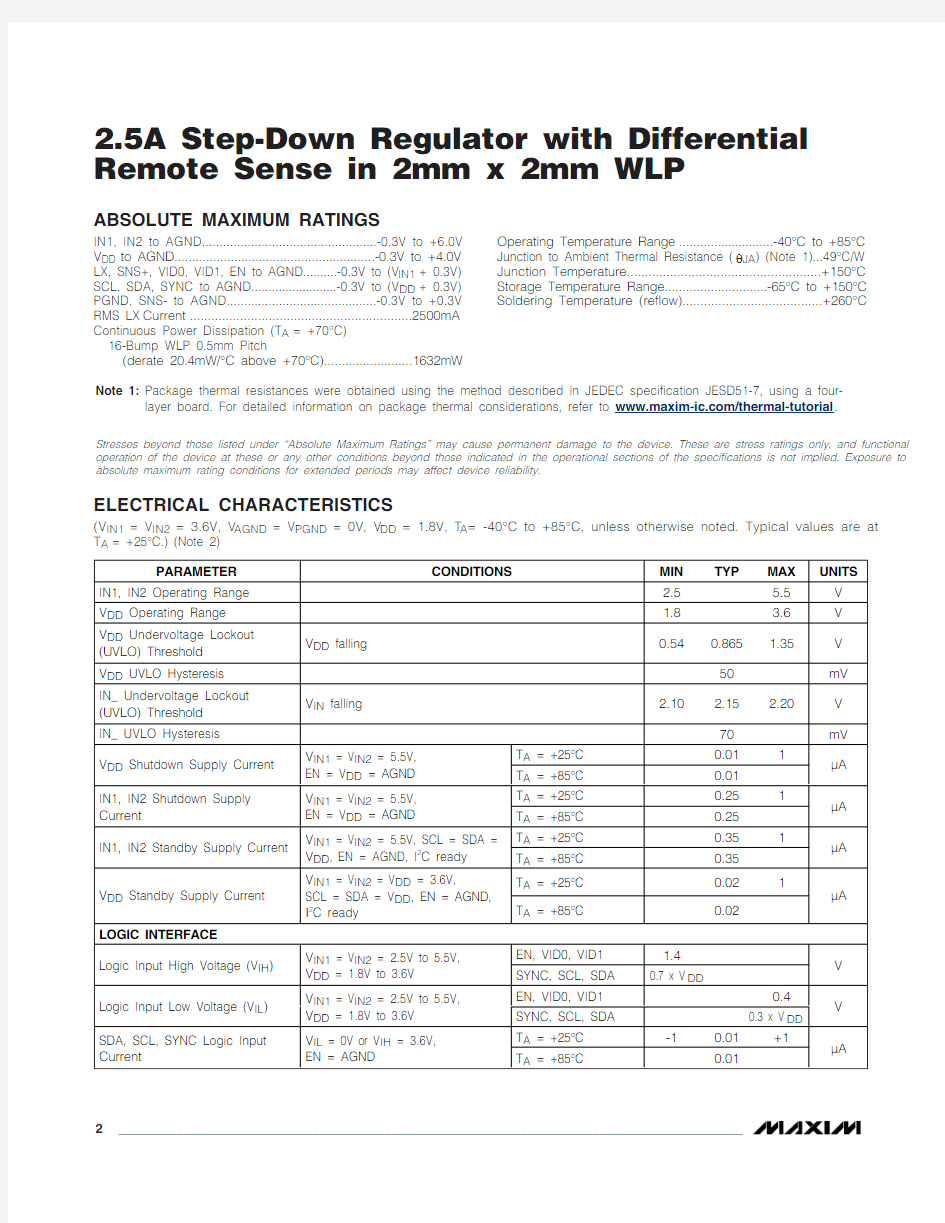
ABSOLUTE MAXIMUM RATINGS
ELECTRICAL CHARACTERISTICS
(V IN1= V IN2= 3.6V, V AGND = V PGND = 0V, V DD = 1.8V, T A = -40°C to +85°C, unless otherwise noted. Typical values are at
Stresses beyond those listed under “Absolute Maximum Ratings” may cause permanent damage to the device. These are stress ratings only, and functional operation of the device at these or any other conditions beyond those indicated in the operational sections of the specifications is not implied. Exposure to absolute maximum rating conditions for extended periods may affect device reliability.
IN1, IN2 to AGND..................................................-0.3V to +6.0V V DD to AGND.........................................................-0.3V to +4.0V LX, SNS+, VID0, VID1, EN to AGND..........-0.3V to (V IN1+ 0.3V)SCL, SDA, SYNC to AGND.........................-0.3V to (V DD + 0.3V)PGND, SNS- to AGND...........................................-0.3V to +0.3V RMS LX Current ..............................................................2500mA Continuous Power Dissipation (T A = +70°C)16-Bump WLP 0.5mm Pitch
(derate 20.4mW/°C above +70°C).........................1632mW
Operating Temperature Range ...........................-40°C to +85°C Junction to Ambient Thermal Resistance (θJA ) (Note 1)...49°C/W Junction Temperature......................................................+150°C Storage Temperature Range.............................-65°C to +150°C Soldering Temperature (reflow).......................................+260°C
Note 1:Package thermal resistances were obtained using the method described in JEDEC specification JESD51-7, using a four-layer board. For detailed information on package thermal considerations, refer to https://www.doczj.com/doc/5d4047054.html,/thermal-tutorial .
MAX8952
2.5A Step-Down Regulator with Differential
Remote Sense in 2mm x 2mm WLP
_______________________________________________________________________________________3
ELECTRICAL CHARACTERISTICS (continued)
(V IN1= V IN2= 3.6V, V AGND = V PGND = 0V, V DD = 1.8V, T A = -40°C to +85°C, unless otherwise noted. Typical values are at T A =+25°C.) (Note 2)
M A X 8952
2.5A Step-Down Regulator with Differential Remote Sense in 2mm x 2mm WLP 4_______________________________________________________________________________________
ELECTRICAL CHARACTERISTICS (continued)
(V
= V = 3.6V, V = V = 0V, V = 1.8V, T = -40°C to +85°C, unless otherwise noted. Typical values are at T =
MAX8952
2.5A Step-Down Regulator with Differential
Remote Sense in 2mm x 2mm WLP
_______________________________________________________________________________________5
ELECTRICAL CHARACTERISTICS (continued)
Note 2:All devices are 100% production tested at T A = +25°C. Limits over the operating temperature range are guaranteed by
design.
M A X 8952
2.5A Step-Down Regulator with Differential Remote Sense in 2mm x 2mm WLP 6_______________________________________________________________________________________
EFFICIENCY vs. LOAD CURRENT (1.0V OUTPUT, SYNC OFF)
LOAD CURRENT (A)E F F I C I E N C Y (%)
10.10.01
0.001
1020304050607080901000
0.0001
10
EFFICIENCY vs. LOAD CURRENT (1.1V OUTPUT, SYNC OFF)
LOAD CURRENT (A)E F F I C I E N C Y (%)
10.10.010.00110
2030
4050607080901000
0.0001
10
EFFICIENCY vs. LOAD CURRENT
(1.4V OUTPUT, SYNC OFF)
LOAD CURRENT (A)
E F F I C I E N C Y (%)
10.10.010.00110
2030
405060708090100
0.0001
10
EFFICIENCY vs. LOAD CURRENT
(1.0V OUTPUT, 26MHz SYNC)
LOAD CURRENT (A)E F F I C I E N C Y (%)
1
0.10.01
0.001
1020304050607080901000
0.0001
10
EFFICIENCY vs. LOAD CURRENT (1.1V OUTPUT, 26MHz SYNC)
LOAD CURRENT (A)E F F I C I E N C Y (%)
1
0.10.01
0.001
10
20
304050607080901000
0.0001
10
EFFICIENCY vs. LOAD CURRENT
(1.4V OUTPUT, 26MHz SYNC)
LOAD CURRENT (A)
E F F I C I E N C Y (%)
10.10.010.001
10
20
30405060708090100
0.0001
10
SWITCHING FREQUENCY vs. LOAD CURRENT
LOAD CURRENT (A)S W I T C H I N G F R E Q U E N C Y (M H z )
2.0
1.5
1.0
0.5
0.51.01.5
2.02.5
3.03.50
2.5
60
35
10
-15
-40
85
3.13.23.33.43.53.63.0
TEMPERATURE (°C)
S W I T C H I N G F R E Q U E N C Y (M H z
)
SWITCHING FREQUENCY vs . TEMPERATURE
NO-LOAD SUPPLY CURRENT vs.SUPPLY VOLTAGE (POWER SAVE)
SUPPLY VOLTAGE (V)
S U P P L Y C U R R E N T (m A )
4.53.50.1
0.2
0.30.40.50.60
2.5 5.5
Typical Operating Characteristics
(Typical Operating Circuit , V IN1= V IN2= 3.6V, V AGND = V PGND = 0V, V OUT = 1.1V, V DD = 1.8V, T A = +25°C, unless otherwise noted.)
MAX8952
2.5A Step-Down Regulator with Differential
Remote Sense in 2mm x 2mm WLP
_______________________________________________________________________________________7
NO-LOAD SUPPLY CURRENT vs.SUPPLY VOLTAGE (FORCED PWM)
SUPPLY VOLTAGE (V)S U P P L Y C U R R E N T (m A )
4.5
3.5
246810121416182002.5
5.5OUTPUT VOLTAGE vs. LOAD CURRENT
LOAD CURRENT (A)O U T P U T V O L T A G E (V )
2.0
1.5
1.0
0.5
1.371.381.391.401.411.421.36
2.5
OUTPUT VOLTAGE vs. LOAD CURRENT
LOAD CURRENT (A)
O U T P U T V O L T A T G E (V ) 2.0
1.5
1.0
0.5
1.0901.095
1.1001.1051.1101.1151.085
2.5
OUTPUT VOLTAGE vs. LOAD CURRENT
LOAD CURRENT (A)
O U T P U T V O L T A T G E (V ) 2.0
1.5
1.0
0.5
0.9850.9900.9951.000
1.0051.010
0.980
2.5
LIGHT LOAD SWITCHING WAVEFORMS
2V/div
20mV/div
200mA/div
V OUT
V LX
I L
2μs/div
MEDIUM LOAD SWITCHING
WAVEFORMS
MAX8952 toc15
2V/div
20mV/div 500mA/div V OUT
V LX I L
200ns/div
500mA LOAD V OUT = 1.3V
HEAVY LOAD SWITCHING WAVEFORMS
MAX8952 toc16
2V/div
20mV/div
1A/div
V OUT
V LX
I L
200ns/div
1.8A LOAD V OUT = 1.3V
Typical Operating Characteristics (continued)
(Typical Operating Circuit , V IN1= V IN2= 3.6V, V AGND = V PGND = 0V, V OUT = 1.1V, V DD = 1.8V, T A = +25°C, unless otherwise noted.)
M A X 8952
2.5A Step-Down Regulator with Differential Remote Sense in 2mm x 2mm WLP 8_______________________________________________________________________________________
LIGHT LOAD STARTUP WAVEFORMS
MAX8952 toc17
100mA/div
500mA/div
1V/div
5V/div V OUT
I IN
I L
V EN
200μs/div
10I LOAD
HEAVY LOAD STARTUP WAVEFORMS
MAX8952 toc18
200mA/div
500mA/div 1V/div
5V/div
V OUT
I IN
I L
V EN
200μs/div
1
I LOAD
400mA
PREBIAS STARTUP WAVEFORMS
(FORCED PWM)
500mV/div
1A/div
5V/div
V OUT
I L
V EN
200μs/div
LINE TRANSIENT RESPONSE (4.2V TO
3.2V TO
4.2V) SYNC OFF
MAX8952 toc20
1V/div
20mV/div
200mA/div
V OUT
I L
20μs/div
300mA LOAD
V IN
LINE TRANSIENT RESPONSE (4.2V TO
3.2V TO
4.2V) 26MHz SYNC
MAX8952 toc21
1V/div
20mV/div
200mA/div
V OUT
I L
20μs/div
300mA LOAD
V IN
LOAD TRANSIENT RESPONSE
(1mA TO 1A)
MAX8952 toc22
50mV/div
500mA/div
1A/div
V OUT
I OUT
I L
40μs/div
Typical Operating Characteristics (continued)
(Typical Operating Circuit , V IN1= V IN2= 3.6V, V AGND = V PGND = 0V, V OUT = 1.1V, V DD = 1.8V, T A = +25°C, unless otherwise noted.)
MAX8952
2.5A Step-Down Regulator with Differential
Remote Sense in 2mm x 2mm WLP
_______________________________________________________________________________________9
LOAD TRANSIENT RESPONSE
(1A to 1mA)
MAX8952 toc23
50mV/div
500mA/div
1A/div
V OUT
I OUT
I L 40μs/div
LOAD TRANSIENT RESPONSE
(5mA TO 1.8A)
MAX8952 toc24
50mV/div
1A/div
1A/div
V OUT
I OUT
I L
40μs/div
LOAD TRANSIENT RESPONSE
(1.8A to 5mA)
MAX8952 toc25
100mV/div
1A/div
1A/div
V OUT
I OUT
I L
20μs/div
SYNCHRONIZATION RESPONSE
(26MHz SYNC)
MAX8952 toc26
200mA/div
2V/div
20mV/div
2V/div V SYNC
V LX
I L
V OUT
1μs/div
FORCED PWM, NO LOAD
OUTPUT VOLTAGE CHANGE RESPONSE
MAX8952 toc27
200mA/div
500mV/div
2V/div
V VID0I
L
V OUT
40μs/div
10I LOAD,POWER SAVE 32mV/μs RAMP
0.9V
0.9V
1.3V
Typical Operating Characteristics
(T A = +25°C, unless otherwise noted.)
M A X 8952
2.5A Step-Down Regulator with Differential Remote Sense in 2mm x 2mm WLP 10______________________________________________________________________________________
MAX8952
2.5A Step-Down Regulator with Differential
Remote Sense in 2mm x 2mm WLP
Figure 1. Block Diagram
Detailed Description
The MAX8952 high-efficiency, 3.25MHz step-down switching regulator delivers up to 2.5A of output cur-rent. The device operates from a 2.5V to 5.5V input voltage range, and the output voltage is I 2C program-mable from 0.77V to 1.40V in 10mV increments. Fully differential remote sense ensures precise DC regula-tion at the load. Total output error is less than 1.5%over load, line, and temperature.
Dynamic Voltage Scaling
The output voltage is dynamically adjusted by use of the VID0 and VID1 logic inputs, allowing selection between four predefined operation modes/voltage configurations.
For each of the different output modes, the following parameters are programmable:
?Output voltage from 0.77V to 1.40V in 10mV steps ?Mode of operation: Forced PWM or power save
?Enable/disable of synchronization of switching
frequency to external clock source
The relation between the VID0/VID1 and operation mode is given by Table 1.
The VID_ inputs have internal pulldown resistors. These pulldown resistors can be disabled through the CON-TROL register after the IC is enabled, achieving lowest possible quiescent current. When EN is low, the CON-TROL register is reset to default, enabling the pulldown resistors.
M A X 8952
2.5A Step-Down Regulator with Differential Remote Sense in 2mm x 2mm WLP 12
______________________________________________________________________________________
Figure 2. Power-Up Sequence Enable
The MAX8952 DC-DC step-down regulator is enabled/disabled using the EN logic input. The EN input is able to handle input voltages up to V IN1, ensur-ing that the EN logic input can be controlled by a wide variety of signals/supplies.
The EN input has an internal pulldown resistor that ensures EN is discharged during off conditions. This pull-down resistor can be disabled through the CONTROL register (see Table 7) once the IC is enabled, achieving lowest possible quiescent current. When EN is low, the CONTROL register is reset to default, enabling the pull-down resistors on EN, VID0, and VID1. See Figures 2and 3 for detailed information on power-up and power-down sequencing and operation mode changes.
DC-DC Regulator Operating Modes
The IC operates in one of four modes determined by the state of the VID_ inputs (see Table 1). At power-up,the IC is set to operate in power-save operation for MODE0 through MODE3. For each of the operation modes, the DC-DC step-down regulator can be set to operate in either power-save mode or forced-PWM mode. This is done by writing to the MODE_ registers (see Table 3 to Table 6). The mode of operation can be changed at any time.
In power-save mode, the MAX8952 PWM switching fre-quency depends on the load current. For medium to high load condition, the IC operates in fixed-frequency PWM mode. For light load conditions, the IC operates in hysteretic mode. The proprietary hysteretic PWM control scheme ensures high efficiency, fast switching,and fast transient response. This control scheme is simple: when the output voltage is below the regula-tion threshold, the error comparator begins a switching cycle by turning on the high-side switch. This switch remains on until the minimum on-time expires and the output voltage is above the regulation threshold plus hysteresis or the inductor current is above the current-limit threshold. Once off, the high-side switch remains off until the minimum off-time expires and the output voltage falls again below the regulation threshold.During the off period, the low-side synchronous rectifi-er turns on and remains on until either the high-side switch turns on again or the inductor current approaches zero. The internal synchronous rectifier eliminates the need for an external Schottky diode.The transition between PWM and hysteretic operation is based on the number of consecutive zero-crossing cycles. When more than 16 consecutive zero-crossing cycles are detected, the DC-DC step-down converter enables the bias for hysteretic operation. Once correct-
MAX8952
2.5A Step-Down Regulator with Differential
Remote Sense in 2mm x 2mm WLP
______________________________________________________________________________________
13
Figure 3a. Shutdown by Pulling V DD Low Before EN
Figure 3b. Shutdown by Pulling EN Low Before V DD
Figure 3c. Shutdown Due to IN1 Undervoltage Lockout
M A X 8952
2.5A Step-Down Regulator with Differential Remote Sense in 2mm x 2mm WLP 14
______________________________________________________________________________________
ly biased and the number of consecutive zero-crossing cycles exceeds 24, the DC-DC step-down converter begins hysteretic operation.
During hysteretic operation, there is a silent DC offset due to the use of valley regulation. See Figure 4.When operating in power-save mode and the load cur-rent is increased so that the number of consecutive zero-crossing cycles is less than 16, the PWM mode is biased. Once fully biased and the number of zero-crossing cycles drops below 8, the DC-DC converter then begins PWM operation. Since there is a delay between the increase in load current and the DC-DC converter starting PWM, the converter supports full current on the output during hysteretic operation.See Figure 5 for a detailed state diagram.
Power-save operation offers improved efficiency at light loads by changing to hysteretic mode, reducing the
switching frequency depending on the load condition.With moderate to heavy loading, the regulator switches at a fixed switching frequency as it does in forced-PWM mode. In power-save mode, the transition from hys-teretic mode to fixed-frequency switching occurs at the load current specified in the following equation:
In forced-PWM mode, the regulator operates with a
constant (3.25MHz or synchronized to external clock source) switching frequency regardless of output load.Forced-PWM mode is ideal for low-noise systems because switching harmonics occur at multiples of the constant switching frequency and are easily filtered.However, light-load power consumption in forced-PWM mode is higher than that of power-save mode.
Soft-Start
The IC includes internal soft-start circuitry that eliminates inrush current at startup, reducing transients on the input source (see the
Typical Operating Charac-
Figure 5. Mode Change for DC-DC Step-Down Converter Figure 4. Output Regulation in Hysteretic Operation
MAX8952
teristics ). Soft-start is particularly useful for high-imped-ance input sources, such as Li+ and alkaline cells.When enabling the IC into a prebiased output, the IC performs a complete soft-start cycle.
Synchronous Rectification
An internal n-channel synchronous rectifier eliminates the need for an external Schottky diode and improves efficiency. The synchronous rectifier turns on during the second half of each switching cycle (off-time). During this time, the voltage across the inductor is reversed,and the inductor current ramps down. In PWM mode,the synchronous rectifier turns off at the end of the switching cycle. In power-save mode, the synchronous rectifier turns off when the inductor current falls below 50mA (typ) or at the end of the switching cycle,whichever occurs first.
Ramp-Rate Control
The MAX8952 output voltage has an actively controlled variable ramp rate, set with the I 2C interface (see Figures 6, 7, and 8). The value set in the RAMP register controls the output voltage ramp rate. The RAMP_DOWN bit controls the active ramp-down behavior in power-save mode. When the regulator is set for power-save mode and the RAMP_DOWN bit is cleared, the ramp-down is not actively controlled, and the regulator output voltage ramps down at the rate
determined by the output capacitance and the external load. Small loads result in an output-voltage decay that is slower than that specified by RAMP; large loads result in an output-voltage decay that is no faster than that specified by RAMP When the RAMP_DOWN bit is set in power-save mode, the zero-cross comparator is disabled during the ramp-down condition. Active ramp-down functionality is inherent in forced-PWM operation.Calculate the maximum and minimum values for the
f SW = 3.25MHz ±10% for PWM operation
f SYNC = frequency of external clock
n = 4 for 13MHz, 6 for 19.2MHz, and 8 for 26MHz
RAMP_CODE = value of the RAMP[2:0] register (see Table 9)
Thermal-Overload Protection
Thermal-overload protection limits total power dissipa-tion in the IC. When internal thermal sensors detect a
Figure 6. Ramp-Up Function
Figure 8. Mode Change Before Final Value is Reached
2.5A Step-Down Regulator with Differential
Remote Sense in 2mm x 2mm WLP
______________________________________________________________________________________
15
M A X 8952
2.5A Step-Down Regulator with Differential Remote Sense in 2mm x 2mm WLP 16______________________________________________________________________________________
die temperature in excess of +160°C (typ), the DC-DC step-down regulator is shut down, allowing the IC to cool. The DC-DC step-down regulator is turned on again after the junction cools by 20°C (typ), resulting in a pulsed output during continuous thermal-overload conditions.
During thermal overload, the I 2C interface remains active and all register values are maintained.
I 2C Interface
An I 2C-compatible, 2-wire serial interface controls the step-down converter output voltage, ramp rate, operat-ing mode, and synchronization. The serial bus consists of a bidirectional serial-data line (SDA) and a serial-clock input (SCL). The master initiates data transfer on the bus and generates SCL to permit data transfer.
I 2C is an open-drain bus. SDA and SCL require pullup resistors (500?or greater). Optional (24?) in series with SDA and SCL protect the device inputs from high-voltage spikes on the bus lines. Series resistors also minimize crosstalk and undershoot on bus signals.
Bit Transfer
One data bit is transferred during each SCL clock cycle. The data on SDA must remain stable during the high period of the SCL clock pulse (see Figure 9).Changes in SDA while SCL is high are control signals (see the START and STOP Conditions section for more information).
Each transmit sequence is framed by a START (S) con-dition and a STOP (P) condition. Each data packet is 9bits long; 8 bits of data followed by the acknowledge
bit. The IC supports data transfer rates with SCL fre-quencies up to 400kHz.
START and STOP Conditions
When the serial interface is inactive, SDA and SCL idle high. A master device initiates communication by issuing a START (S) condition. A START condition is a high-to-low transition on SDA with SCL high. A STOP (P) condition is a low-to-high transition on SDA, while SCL is high (Figure 10).
A START condition from the master signals the begin-ning of a transmission to the IC. The master terminates transmission by issuing a not acknowledge followed by
Figure 9. I C Bit Transfer
Figure 10. I C START and STOP Conditions
MAX8952
2.5A Step-Down Regulator with Differential
Remote Sense in 2mm x 2mm WLP
______________________________________________________________________________________17
a STOP condition (see the Acknowledge section for more information). The STOP condition frees the bus.To issue a series of commands to the slave, the master can issue REPEATED START (Sr) commands instead of a STOP command to maintain control of the bus. In general, a REPEATED START command is functionally equivalent to a regular START command.
When a STOP condition or incorrect address is detect-ed, the IC internally disconnects SCL from the serial interface until the next START condition, minimizing dig-ital noise and feedthrough.
System Configuration
A device on the I 2C bus that generates a message is called a transmitter and a device that receives the mes-sage is a receiver. The device that controls the mes-sage is the master and the devices that are controlled by the master are called slaves. See Figure 11.
Acknowledge
The number of data bytes between the START and STOP conditions for the transmitter and receiver are unlimited. Each 8-bit byte is followed by an acknowl-edge bit. The acknowledge bit is a high-level signal put on SDA by the transmitter during which time the master generates an extra acknowledge-related clock pulse. A slave receiver that is addressed must generate an acknowledge after each byte it receives. Also, a master receiver must generate an acknowledge after each byte it receives that has been clocked out of the slave transmitter. See Figure 12.
The device that acknowledges must pull down the DATA line during the acknowledge clock pulse, so that the DATA line is stable low during the high period of the
acknowledge clock pulse (setup and hold times must also be met). A master receiver must signal an end of data to the transmitter by not generating an acknowl-edge on the last byte that has been clocked out of the slave. In this case, the transmitter must leave SDA high to enable the master to generate a STOP condition.
Register Reset
The I 2C resisters reset back to their default values when the voltage at either IN1 or V DD drops below the corresponding UVLO threshold (see the Electrical Characteristics table).
Update of Output Operation Mode
If updating the output voltage or Operation Mode regis-ter for the mode that the IC is currently operating in, the
Figure 11. I
CMaster/Slave Configuration
Figure 12. I C Acknowledge
M A X 8952
2.5A Step-Down Regulator with Differential Remote Sense in 2mm x 2mm WLP 18
______________________________________________________________________________________
output voltage/operation mode is updated at the same time the IC sends the acknowledge for the I 2C data byte (see Figure 13).
Slave Address
A bus master initiates communication with a slave device (MAX8952) by issuing a START condition fol-lowed by the slave address. The slave address byte consists of 7 address bits (1100 000x) and a read/write bit (R/W ). After receiving the proper address, the IC issues an acknowledge by pulling SDA low during the ninth clock cycle.
Other slave addresses can be assigned. Contact the factory for details.
Write Operations
The IC recognizes the write byte protocol as defined in the SMBus? specification and shown in Figures 14a and 14b. The write byte protocol allows the I 2C master device to send 1 byte of data to the slave device. The write byte protocol requires a register pointer address for the sub-sequent write. The IC acknowledges any register pointer even though only a subset of those registers actually exists in the device. The write byte protocol is as follows:1)The master sends a start command.
2)The master sends the 7-bit slave address followed
by a write bit.
3)The addressed slave asserts an acknowledge by
pulling SDA low.
4)The master sends an 8-bit register pointer.5)The slave acknowledges the register pointer.6)The master sends a data byte.
7)The slave acknowledges the data byte.8)The slave updates with the new data.9)The master sends a STOP condition.
In addition to the write-byte protocol, the IC can write to multiple registers as shown in Figure 14b. This protocol allows the I 2C master device to address the slave only once and then send data to a sequential block of regis-ters starting at the specified register pointer.
Use the following procedure to write to a sequential block of registers:
1)The master sends a start command.
2)The master sends the 7-bit slave address followed
by a write bit.
3)The addressed slave asserts an acknowledge by
pulling SDA low.
4)The master sends the 8-bit register pointer of the
first register to write.
5)The slave acknowledges the register pointer.6)The master sends a data byte.
7)The slave acknowledges the data byte.
8)The slave updates with the new data.
9)Steps 6 to 8 are repeated for as many registers in
the block, with the register pointer automatically incremented each time.
10)The master sends a STOP condition.
Read Operations
The method for reading a single register (byte) is shown in Figure 15a. To read a single register:
Figure 13. Update Output Operation
SMBus is a trademark of Intel Corp.
MAX8952
2.5A Step-Down Regulator with Differential
Remote Sense in 2mm x 2mm WLP
______________________________________________________________________________________19
1)The master sends a start command.
2)The master sends the 7-bit slave address followed
by a write bit.
3)The addressed slave asserts an acknowledge by
pulling SDA low.
4)The master sends an 8-bit register pointer.5)The slave acknowledges the register pointer.6)The master sends a repeated START condition.
7)The master sends the 7-bit slave address followed
by a read bit.
8)The slave asserts an acknowledge by pulling SDA low.9)The slave sends the 8-bit data (contents of the
register).
10)The master asserts a not acknowledge by keeping
SDA high.
11)The master sends a STOP condition.
In addition, the IC can read a block of multiple sequential registers as shown in Figure 15b. Use the following pro-cedure to read a sequential block of registers:1)The master sends a start command.
2)The master sends the 7-bit slave address followed
by a write bit.
3)The addressed slave asserts an acknowledge by
pulling SDA low.
4)The master sends an 8-bit register pointer of the
first register in the block.
5)The slave acknowledges the register pointer.6)The master sends a repeated START condition.
7)The master sends the 7-bit slave address followed
by a read bit.
8)The slave asserts an acknowledge by pulling SDA low.9)The slave sends the 8-bit data (contents of the reg-ister).
10)The master asserts an acknowledge by pulling SDA
low when there is more data to read, or a not acknowledge by keeping SDA high when all data has been read.
11)Steps 9 and 10 are repeated for as many registers
in the block, with the register pointer automatically incremented each time.
12)The master sends a STOP condition.
Figures 14a and 14b. Writing to the IC
M A X 8952
2.5A Step-Down Regulator with Differential Remote Sense in 2mm x 2mm WLP 20______________________________________________________________________________________
Figures 15a and 15b. Reading from the IC
Figure 16. I C Timing Diagram