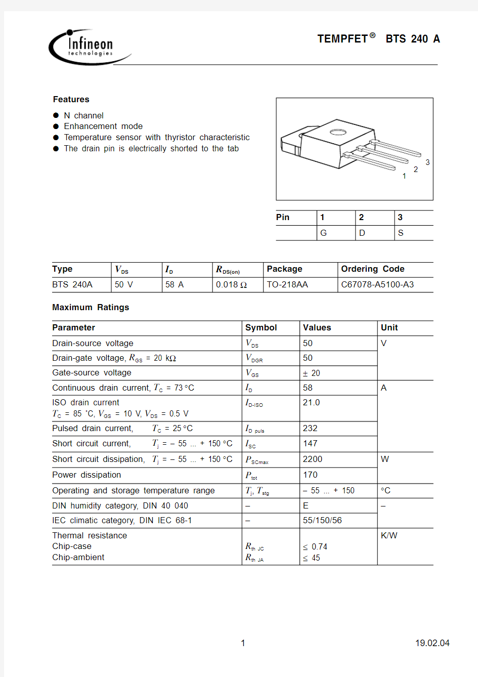
Electrical Characteristics
at T j = 25°C, unless otherwise specified.Parameter
Symbol
Values Unit
min.
typ.
max.
Static Characteristics
Drain-source breakdown voltage V GS = 0, I D = 0.25 mA V (BR)DSS
50
––V
Gate threshold voltage V GS =V DS , I D = 1 mA
V GS(th)
2.5
3.0
3.5
Zero gate voltage drain current V GS = 0 V,V DS = 50 V
T j = 25°C T j = 125°C I DSS
––
0.110
1.0100
μA
Gate-source leakage current V GS = 20 V,V DS = 0
T j = 25°C T j = 150°C I GSS
––
102.01004.0nA μA Drain-source on-state resistance V GS = 10 V , I D =47 A R DS(on)
–
0.012
0.018
?
Dynamic Characteristics Forward transconductance
V DS ≥ 2×I D ×R DS(on)max ,I D = 47 A g fs
20.0
43.0–
S Input capacitance
V GS = 0, V DS = 25 V,f = 1 MHz C iss –
2.9 4.3nF
Output capacitance
V GS = 0, V DS = 25 V,f = 1 MHz C oss
–
1.4
2.1Reverse transfer capacitance V GS = 0, V DS = 25 V,f = 1 MHz
C rss
–0.50.8Turn-on time t on , (t on =t d(on) +t r )V CC = 30 V,V GS = 10 V,I D = 3 A,R GS = 50?t d(on)–5075ns
t
r
–150230Turn-off time t off , (t off =t d(off) +t f )V CC = 30 V,V GS = 10 V,I D = 3 A,R GS = 50?t d(off)–350560t
f
–
250
330
Electrical Characteristics (cont ’d)
at T j = 25°C, unless otherwise specified.Parameter
Symbol
Values Unit
min.
typ.
max.
Reverse Diode
Continuous source current I S ––58A Pulsed source current I SM –
–
232
Diode forward on-voltage I F = 58 A, V GS = 0 V
V SD
– 1.4 1.8
V
Reverse recovery time
I F =I S , d i F /d t = 100 A/μs,V R = 30 V t rr
–
100–
ns Reverse recovery charge
I F =I S , d i F /d t = 100 A/μs,V R = 30 V Q rr
–
0.3
–
μC
Temperature Sensor
Forward voltage
I TS(on) = 10 mA,T j = – 55 ... + 150°C Sensor override,t p ≤ 100μs T j = – 55 ... + 160°C V TS(on)
0.7–
1.4– 1.510
V
Forward current T j = – 55 ... + 150°C
Sensor override,t p ≤ 100μs T j = – 55 ... + 160°C I TS(on)
––
––10600mA
Holding current,V TS(off) = 5 V,T j = 25°C T j = 150°C
I H 0.050.050.1
0.20.50.3
Switching temperature V TS = 5 V
T TS(on)
150
––
°C
Turn-off time
V TS = 5 V,I TS(on) = 2 mA
t off
0.5
–
2.5
μs
Examples for short-circuit protection
at T j = – 55 ... + 150°C, unless otherwise specified.
Parameter Symbol Examples Unit
12–
Drain-source voltage V DS1530–V Gate-source voltage V GS 6.4 5.1–
Short-circuit current I SC<147<67–A Short-circuit dissipation P SC<2200<2000–W Response time
T j = 25°C, before short circuit
t
SC(off)
<25<25–
ms
Short-circuit protection I SC =f (V DS) Parameter:V GS
Diagram to determine I SC for T j=–55...+150°C Max. gate voltage V GS(SC) =f (V DS) Parameter:T j=– 55... +150°C
Max. power dissipation P tot =f (T C) Typical output characteristics I D =f (V DS) Parameter:t p=80μs Typ. drain-source on-state resistance R
DS(on)
=f (I D)
Parameter:V GS
Safe operating area I D =f (V DS) Parameter:D = 0.01,T C=25°C
Drain-source on-state resistance
R
DS(on)
=f (T j)
Parameter:I D=47 A,V GS = 10 V (spread)
Typ. transfer characteristic
I
D
=f (V GS)
Parameter:t p = 80μs,V DS = 25 V Gate threshold voltage V GS(th) =f (T j) Parameter:V DS =V GS,I D=1 mA Typ. transconductance g fs =f (I D) Parameter:t p = 80μs,V DS = 25 V
Continuous drain current I D=f (T C) Parameter:V GS≥ 10 V
Typ. gate-source leakage current I
GSS
=f (T C)
Parameter:V GS = 20 V,V DS = 0Forward characteristics of reverse diode I
F
=f (V SD)
Parameter:T j,t p = 80μs (spread)
Typ. capacitances C =f (V DS) Parameter:V GS = 0,f=1 MHz
Transient thermal impedance Z thJC =f (t p) Parameter:D =t p/T
TO-218 AA Ordering Code Standard C67078-S5100-A3
Edition 04.97
Published by Infineon Technologies AG,
St.-Martin-Strasse 53,
D-81541 München, Germany
? Infineon Technologies AG 2000.
All Rights Reserved.
Attention please!
The information herein is given to describe certain components and shall not be considered as warranted characteristics.
Terms of delivery and rights to technical change reserved.
We hereby disclaim any and all warranties, including but not limited to warranties of non-infringement, regarding circuits, descriptions and charts stated herein.
Infineon Technologies is an approved CECC manufacturer.
Information
For further information on technology, delivery terms and conditions and prices please contact your nearest Infineon Technologies Office in Germany or our Infineon T echnologies Representatives worldwide (see address list).
Warnings
Due to technical requirements components may contain dangerous substances. For information on the types in question please contact your nearest Infineon T echnologies Office.
Infineon T echnologies Components may only be used in life-support devices or systems with the express written approval of Infineon Technologies, if a failure of such components can reasonably be expected to cause the failure of that life-support device or system, or to affect the safety or effectiveness of that device or system. Life support devices or systems are intended to be implanted in the human body, or to support and/or maintain and sustain and/or protect human life. If they fail, it is reasonable to assume that the health of the user or other persons may be endangered.