General Description
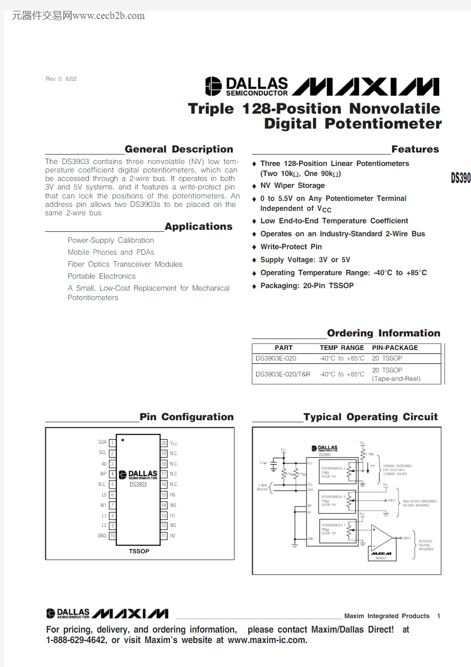
The DS3903 contains three nonvolatile (NV) low tem-perature coefficient digital potentiometers, which can be accessed through a 2-wire bus. It operates in both 3V and 5V systems, and it features a write-protect pin that can lock the positions of the potentiometers. An address pin allows two DS3903s to be placed on the same 2-wire bus.
Applications
Power-Supply Calibration Mobile Phones and PDAs Fiber Optics Transceiver Modules Portable Electronics
A Small, Low-Cost Replacement for Mechanical Potentiometers
Features
?Three 128-Position Linear Potentiometers (Two 10k ?, One 90k ?)?NV Wiper Storage
?0 to 5.5V on Any Potentiometer Terminal Independent of V CC ?Low End-to-End Temperature Coefficient ?Operates on an Industry-Standard 2-Wire Bus ?Write-Protect Pin ?Supply Voltage: 3V or 5V
?Operating Temperature Range: -40°C to +85°C ?Packaging: 20-Pin TSSOP
DS3903
Triple 128-Position Nonvolatile
Digital Potentiometer
_____________________________________________Maxim Integrated Products 1
Pin Configuration
Typical Operating Circuit
Ordering Information
Rev 0; 6/02
For pricing, delivery, and ordering information,please contact Maxim/Dallas Direct!at 1-888-629-4642, or visit Maxim’s website at https://www.doczj.com/doc/5c327457.html,.
D S 3903
Triple 128-Position Nonvolatile Digital Potentiometer 2______________________________________________________________________
ABSOLUTE MAXIMUM RATINGS
RECOMMENDED DC OPERATING CONDITIONS
(T
= -40°to +85°C)
Stresses beyond those listed under “Absolute Maximum Ratings” may cause permanent damage to the device. These are stress ratings only, and functional operation of the device at these or any other conditions beyond those indicated in the operational sections of the specifications is not implied. Exposure to absolute maximum rating conditions for extended periods may affect device reliability.
Voltage on V CC Pin Relative to Ground.................-0.5V to +6.0V Voltage on SDA, SCL, A0, and WP
Relative to Ground...........................................................-0.5V to
V CC + 0.5V
Voltage on L0, L1, L2, W0, W1, W2, H0, H1, and
H2 Relative to Ground...........................................-0.5V to +6.0V
Current Through W0, W1, and W2......................................±4mA Operating Temperature Range ...........................-40°C to +85°C Programming Temperature Range.........................0°C to +70°C Storage Temperature Range.............................-55°C to +125°C Soldering Temperature....................See IPC/JEDEC J-STD-020A
Specification
DC ELECTRICAL CHARACTERISTICS
DS3903
Triple 128-Position Nonvolatile
Digital Potentiometer
_____________________________________________________________________3
AC ELECTRICAL CHARACTERISTICS
(V CC = 2.7V to 5.5V, T A = -40°C to +85°C.)
(V CC = 2.7V to 5.5V, T A = -40°C to +85°C.)
D S 3903
Triple 128-Position Nonvolatile Digital Potentiometer 4______________________________________________________________________
Note 1:All voltages are referenced to ground.
Note 2:
I STBY specified for V CC equal to 3.0V and 5.0V while control port logic pins are driven to the appropriate logic levels. Appropriate logic levels specify that logic inputs are within a 0.5V of ground or V CC for the corresponding inactive state. WP must be disconnected or connected high.
Note 3:I/O pins of fast mode devices must not obstruct the SDA and SCL lines if V CC is switched off.
Note 4:
A fast mode device can be used in a standard mode system, but the requirement t SU:DAT > 250ns must then be met. This is automatically the case if the device does not stretch the low period of the SCL signal.If such a device does stretch the low period of the SCL signal, it must output the next data bit to the SDA line t RMAX + t SU:DAT = 1000ns + 250ns = 1250ns before the SCL line is released.Note 5:After this period, the first clock pulse is generated.
Note 6:The maximum t HD:DAT has only to be met if the device does not stretch the low period (t LOW ) of the SCL signal.
Note 7: A device must internally provide a hold time of at least 300ns for the SDA signal (referred to the V IN MIN of the SCL signal) in order to bridge the undefined region of the falling edge of SCL.
Note 8:C B —total capacitance of one bus line in picofarads, timing referenced to 0.9 x V CC and 0.1 x V CC .Note 9:EEPROM write begins after a stop condition occurs.
Note 10:Absolute linearity is used to measure expected wiper voltage as determined by wiper position in a voltage-divider configuration.
Note 11:
Relative linearity is used to determine the change of wiper voltage between two adjacent wiper positions in a voltage-divider configuration.
Typical Operating Characteristics
(V CC = 5.0V, 10k ?plots apply to both pot0 and pot2, T A = +25°C unless otherwise noted.)
10
2030405060708090100
W-L RESISTANCE vs. WIPER SETTING (90k ?)
D S 3903 t o c 03
WIPER SETTING
W -L R E S I S T A N C E (k ?)
125
100
75
50
25
W-L RESISTANCE vs. WIPER SETTING (10k ?)
D S 3903 t o c 02
WIPER SETTING
W -L R E S I S T A N C E (k ?)
125
100
75
50
25
02468100
STANDBY SUPPLY CURRENT
vs. TEMPERATURE
TEMPERATURE (°C)
S U P P L Y C U R R E N T (μA )
5040-30-20-101020030204060801001201401600
-40607080
DS3903
Triple 128-Position Nonvolatile
Digital Potentiometer
_____________________________________________________________________5
END-TO-END RESISTANCE PERCENT CHANGE FROM 25°C vs. TEMPERATURE (90k ?)
D S 3903 t o c 09
TEMPERATURE (°C)
% C H A N G E
80
705060-10010203040-30-20-0.6-0.4-0.200.20.40.60.81.0-0.8-1.0
-40END-TO-END RESISTANCE PERCENT CHANGE FROM 25°C vs. TEMPERATURE (10k ?)
D S 3903 t o c 08
TEMPERATURE (°C)
% C H A N G E
80
705060-10010203040-30-20-0.6-0.4-0.200.20.40.60.81.0
-0.8-1.0
-40VOLTAGE-DIVIDER PERCENT CHANGE FROM 25°C vs. TEMPERATURE (10k ?)
TEMPERATURE (°C)% C H A N G E (F R O M 25°C )
80
705060-10010203040-30-20-0.04-0.03-0.02-0.0100.01
0.020.030.04-0.05-0.06
-40VOLTAGE-DIVIDER PERCENT CHANGE FROM 25°C vs. TEMPERATURE (10k ?
)
TEMPERATURE (°C)
% C H A N G E (F R O M 25°C )
80
705060-1001020
3040-30-20-0.04
-0.0200.020.040.060.080.100.12
-0.06
-40WIPER RESISTANCE vs. WIPER VOLTAGE (90k ?)
WIPER VOLTAGE (V)
W I P E R R
E S I S T A N C E (?)
3
4
5
2
1
5010015020025030035000
WIPER RESISTANCE vs. WIPER VOLTAGE (10k ?)
WIPER VOLTAGE (V)
W I P E R R E S I S T A N C E (?)
3
4
5
2
1
5010015020025030035000
Typical Operating Characteristics (continued)
(V CC = 5.0V, 10k ?plots apply to both pot0 and pot2, T A = +25°C unless otherwise noted.)
VOLTAGE-DIVIDER ABSOLUTE LINEARITY
vs. WIPER SETTING (10k ?)
D S 3903 t o c 11
WIPER SETTING
A B S O L U T E L I N E A R T I Y (L S B )
100
80
60
40
20
0.04
0.08
0.12
0.16
0.20
00
120
VOLTAGE-DIVIDER RELATIVE LINEARITY
vs. WIPER SETTING (10k ?)
D S 3903 t o c 10
WIPER SETTING
R E L A T I V E L I N E A R T I Y (L S B )
100
80
60
40
20
0.010.020.03
0.040.050
120
D S 3903
Triple 128-Position Nonvolatile Digital Potentiometer 6______________________________________________________________________
Typical Operating Characteristics (continued)
(VCC = 5.0V, 10k ?plots apply to both pot0 and pot2, TA = +25°C unless otherwise noted.)
VOLTAGE-DIVIDER ABSOLUTE LINEARITY
vs. WIPER SETTING (90k ?)
D S 3903 t o c 13
WIPER SETTING
A B S O L U T E L I N E A R T I Y (L S B )
100
80
60
40
20
0.04
0.08
0.12
0.16
0.20
00
120
VOLTAGE-DIVIDER RELATIVE LINEARITY
vs. WIPER SETTING (90k ?)
D S 3903 t o c 12
WIPER SETTING
R E L A T I V E L I N E A R T I Y (L S B )
100
80
60
40
20
0.010.020.030.040.0500
120
Detailed Description
The DS3903 contains three NV, low-temperature coeffi-cient digital potentiometers. It is accessible through a 2-wire bus, and it serves as a small, low-cost replace-ment for designs using mechanical potentiometers. The low end-to-end resistance temperature coefficient is especially beneficial for designs using a digital poten-tiometer as a 2-terminal variable resistor.
It operates in both 3V and 5V systems, and it features a write-protect pin that can lock the positions of the potentiometers. The address pin allows two DS3903s to be placed on the same 2-wire bus.
With its low cost and small board space, the DS3903 is well tailored to replace larger mechanical potentiome-ters. This allows the automation of calibration in many instances because the 2-wire interface can easily be adjusted by test hardware. Once the system is calibrat-ed, the write-protect pin can be disconnected and the potentiometers retain their settings.
Potentiometer Memory
Organization
The potentiometers of the DS3903 are addressed by communicating with the registers in Table 1.
Device Operation
Clock and Data Transitions
The SDA pin is normally pulled high with an external resistor or device. Data on the SDA pin can only change during SCL low time periods. Data changes during SCL high periods indicates a start or stop condition depend-ing on the conditions discussed below. See the timing diagrams for further details (Figures 2 and 3).
Start Condition
A high-to-low transition of SDA with SCL high is a start condition, which must precede any other command. See the timing diagrams for further details (Figures 2 and 3).
Stop Condition
A low-to-high transition of SDA with SCL high is a stop condition. After a read sequence, the stop command places the DS3903 into a low-power mode. See the tim-ing diagrams for further details (Figures 2 and 3).
Acknowledge
All address and data bytes are transmitted through a serial protocol. The DS3903 pulls the SDA line low dur-ing the ninth clock pulse to acknowledge that it has received each word.
Standby Mode
The DS3903 features a low-power mode that is auto-matically enabled after power-on, after a stop com-mand, and after the completion of all internal operations.
Memory Reset
After any interruption in protocol, power loss, or system reset, the following steps reset the DS3903:1)Clock up to nine cycles.2)Look for SDA high in each cycle while SCL is high.3)
Create a start condition while SDA is high.
Device Addressing
The DS3903 must receive an 8-bit device address word following a start condition to enable a specific device for a read or write operation. The address word is clocked into the DS3903 MSB to LSB. The address
DS3903
Triple 128-Position Nonvolatile
Digital Potentiometer
_____________________________________________________________________
7
*The most significant bit of each potentiometer position value is ignored. Writing a value greater than 7Fh to any of the potentiometer registers results in a valid 7-bit position, without regard to the value of the most significant bit. Example: position 0x82 is the same as position 0x02.
D S 3903
Triple 128-Position Nonvolatile Digital Potentiometer 8______________________________________________________________________
word consists of 101000 binary followed by A0 then the R/W bit. If the R/W bit is high, a read operation is initiat-ed. If the R/W bit is low, a write operation is initiated.For a device to become active, the value of A0 must be the same as the hard-wired address pins on the DS3903. Upon a match of written and hard-wired addresses, the DS3903 outputs a zero for one clock cycle as an acknowledge. If the address does not match, the DS3903 returns to a low-power mode.
Write Operations
After receiving a matching device address byte with the R/W bit set low, the device goes into the write mode of operation. The master must transmit an 8-bit EEPROM memory address to the device to define the address where the data is to be written. After the byte has been received, the DS3903 transmits a zero for one clock cycle to acknowledge the memory address has been received. The master must then transmit an 8-bit data word to be written into this memory address. The DS3903 again transmits a zero for one clock cycle to acknowledge the receipt of the data byte. At this point,the master must terminate the write operation with a stop condition. The DS3903 then enters an internally timed
DS3903
Triple 128-Position Nonvolatile
Digital Potentiometer
_____________________________________________________________________9
write process t w to the EEPROM memory. All inputs are disabled during this write cycle.
The DS3903 is capable of an 8-byte page write. A page write is initiated the same way as a byte write, but the master does not send a stop condition after the first data byte. Instead, after the slave acknowledges the data byte has been received, the master can send up to seven more data bytes using the same nine-clock sequence. After a write to the last byte in the page, the address returns to the beginning of the same page.The master must then terminate the write cycle with a stop condition or the data clocked into the DS3903 is not latched into EEPROM. Note that in order for eight bytes to be stored sequentially (and to prevent looping around), the address byte must be set to the beginning of the desired page (three LSBs of the address are 0).For detailed information concerning page operations,see the Potentiometer Memory Organization section.
Acknowledge Polling
Once the internally timed write has started and the DS3903 inputs are disabled, acknowledge polling can be initiated. The process involves transmitting a start condition followed by the device address. The R/W bit signifies the type of operation that is desired. The read or write sequence is only allowed to proceed if the internal write cycle has completed and the DS3903responds with a zero.
Read Operations
After receiving a matching address byte with the R/W bit set high, the device goes into the read mode of opera-tion. There are three read operations: current address read, random read, and sequential address read.Current Address Read
The DS3903 has an internal address register that main-tains the address used during the last read or write operation, incremented by one. This data is maintained as long as V CC is valid. If the most recent address was the last byte in memory, then the register resets to the first address. This address stays valid between opera-tions as long as power is available.
Once the device address is clocked in and acknowl-edged by the DS3903 with the R/W bit set to high, the current address data word is clocked out. The master does not respond with a zero, but does generate a stop condition afterwards.
Random Address Read
A random read requires a dummy byte write sequence to load in the data word address. Once the device address and data address bytes are clocked in by the master, and acknowledged by the DS3903, the master
must generate another start condition. The master now initiates a current address read by sending the device address with the R/W bit set high. The DS3903acknowledges the device address and serially clocks out the data byte.
Sequential Address Read
Sequential reads are initiated by either a current address read or a random address read. After the mas-ter receives the first data byte, the master responds with an acknowledge. As long as the DS3903 receives this acknowledge after a byte is read, the master can clock out additional data words from the DS3903. After reaching address FFh, it resets to address 00h.
The sequential read operation is terminated when the master initiates a stop condition. The master does not respond with a zero.
For a more detailed description of 2-wire theory of operation, see the following section.
2-Wire Serial Port Operation
The 2-wire serial port interface supports a bidirectional data transmission protocol with device addressing. A device that sends data on the bus is defined as a trans-mitter, and a device receiving data as a receiver. The device that controls the message is called a “master.”The devices that are controlled by the master are “slaves.” The bus must be controlled by a master device that generates the serial clock (SCL), controls the bus access, and generates the start and stop con-ditions. The DS3903 operates as a slave on the 2-wire bus. Connections to the bus are made through the open-drain I/O lines, SDA and SCL. The following I/O terminals control the 2-wire serial port: SDA, SCL, and A0. Timing diagrams for the 2-wire serial port can be found in Figures 2 and 3. Timing information for the 2-wire serial port is provided in the AC Elec tric al Characteristics table for 2-wire serial communications.
D S 3903
Triple 128-Position Nonvolatile Digital Potentiometer
10
_____________________________________________________________________
The following bus protocol has been defined:
Data transfer can be initiated only when the bus is not busy.
During data transfer, the data line must remain stable whenever the clock line is high. Changes in the data line while the clock line is high are interpreted as con-trol signals.
Accordingly, the following bus conditions have been defined:
Bus Not Busy: Both data and clock lines remain high.Start Data Transfer: A change in the state of the data line from high to low while the clock is high defines a start condition.
Stop Data Transfer: A change in the state of the data line from low to high while the clock line is high defines the stop condition.
Data Valid: The state of the data line represents valid data when, after a start condition, the data line is stable for the duration of the high period of the clock signal. The data on the line can be changed during the low period of the clock signal. There is one clock pulse per bit of data.Figures 2 and 3 detail how data transfer is accomplished on the 2-wire bus. Depending upon the state of the R/W bit, two types of data transfer are possible.
Each data transfer is initiated with a start condition and terminated with a stop condition. The number of data bytes transferred between start and stop conditions is not limited and is determined by the master device. The information is transferred byte-wise and each receiver acknowledges with a ninth bit.
Within the bus specifications, a regular mode (100kHz clock rate) and a fast mode (400kHz clock rate) are defined. The DS3903 works in both modes.
Acknowledge: Each receiving device, when addressed, is obliged to generate an acknowledge after the byte has been received. The master device must generate an extra clock pulse that is associated with this acknowledge bit.
A device that acknowledges must pull down the SDA line during the acknowledge clock pulse in such a way that the SDA line is a stable low during the high period of the acknowledge-related clock pulse. Of course,setup and hold times must be taken into account. A master must signal an end of data to the slave by not generating an acknowledge bit on the last byte that has been clocked out of the slave. In this case, the slave must leave the data line high to enable the master to generate the stop condition.
Data transfer from a master transmitter to a slave
receiver. The first byte transmitted by the master is the command/control byte. Next follows a number of data bytes. The slave returns an acknowledge bit after each received byte.
Data transfer from a slave transmitter to a master receiver. The master transmits the first byte (the com-mand/control byte) to the slave. The slave then returns an acknowledge bit. Next follows a number of data bytes transmitted by the slave to the master. The mas-ter returns an acknowledge bit after all received bytes other than the last byte. At the end of the last received byte, a not acknowledge can be returned.
The master device generates all serial clock pulses and the start and stop conditions. A transfer is ended with a stop condition or with a repeated start condition. Since a repeated start condition is also the beginning of the next serial transfer, the bus is not released.
The DS3903 can operate in the following three modes:1)Slave Receiver Mode:Serial data and clock are
received through SDA and SCL, respectively. After each byte is received, an acknowledge bit is trans-mitted. Start and stop conditions are recognized as the beginning and end of a serial transfer. Address recognition is performed by hardware after the slave (device) address and direction bit has been received.
2)Slave Transmitter Mode:The first byte is received
and handled as in the slave receiver mode.However, in this mode the direction bit indicates that the transfer direction is reversed. Serial data is transmitted on SDA by the DS3903 while the serial clock is input on SCL. Start and stop conditions are recognized as the beginning and end of a serial transfer.
3)Slave Address:Command/control byte is the first
byte received following the start condition from the master device. The command/control byte consists of a 6-bit control code. For the DS3903, this is set as 101000binary for read/write operations. The next bit of the command/control byte is the device select bit or slave address (A0). It is used by the master device to select which of two devices is to be accessed. When reading or writing the DS3903,the device-select bits must match the device-select pin (A0). The last bit of the command/control byte (R/W) defines the operation to be performed. When set to a ‘1’, a read operation is selected, and when set to a ‘0’, a write operation is selected.Following the start condition, the DS3903 monitors the SDA bus checking the device type identifier being transmitted. Upon receiving the 101000 control code,
DS3903
Triple 128-Position Nonvolatile
Digital Potentiometer
Maxim c annot assume responsibility for use of any c irc uitry other than c irc uitry entirely embodied in a Maxim produc t. No c irc uit patent lic enses are implied. Maxim reserves the right to change the circuitry and specifications without notice at any time.
Maxim Integrated Products, 120 San Gabriel Drive, Sunnyvale, CA 94086 408-737-7600 ____________________11?2002 Maxim Integrated Products
Printed USA
is a registered trademark of Maxim Integrated Products.
the appropriate device address bit, and the read/write bit, the slave device outputs an acknowledge signal on the SDA line.
Applications Information
Power-Supply Decoupling
To achieve the best results when using the DS3903,decouple the power supply with a 0.01μF or 0.1μF capacitor. Use a high-quality ceramic surface-mount capacitor if possible. Surface-mount components mini-mize lead inductance, which improves performance,and ceramic capacitors tend to have adequate high-frequency response for decoupling applications.
Write Protection
The write-protect pin has an internal pullup resistor. To be able to adjust the potentiometers’ position, this pin must be grounded. This pin can be left floating or con-nected to V CC to write protect the potentiometer posi-tions.
Wiper Resistance and Wiper Current Limit
Two substantial differences between digital poten-tiometers and mechanical potentiometers are the wiper resistance and the wiper current limit. The wiper resis-tance (R W ) is a result of the interconnecting materials on the IC between the internal resistive elements and the wiper pin. This can be modelled by using an ideal potentiometer, with a resistance of R W connected between the ideal wiper and wiper terminal of the digi-tal potentiometer. One final note about the wiper resis-tance is that it has a high temperature coefficient (approximately +3000PPM), which can be noticeable in certain circuit configurations.
The wiper current limit (I W ) is also due to the intercon-necting materials between the internal resistive ele-ments and the wiper terminal. While it may be possible to exceed this value for a short period without prob-lems, exceeding the wiper current limit is a long-term reliability problem.
Both characteristics can be minimized in designs by connecting the wiper terminal to high-impedance loads. This reduces both the current through the wiper and the voltage drop across the wiper resistance.
Using a Potentiometer as a
Variable Resistor
There are two ways to make a digital potentiometer into a variable resistor. The first is to short the wiper terminal to the high- or low-side terminal. This places wiper resistance in parallel with the resistance from the wiper to the high or low side of the potentiometer. The advan-tage of this method is that it reduces the current through the wiper, which is advantageous if the current is approaching the wiper current limit. The disadvan-tage is that the wiper resistance makes the resistance versus position nonlinear, particularly for low-resistance values.
The second way is to attach the wiper terminal, and either the low- or high-side terminal. The unattached terminal is connected to the wiper by the resistance internal to the part, and stays at the same voltage as the wiper. This method provides a linear resistance ver-sus position function, but it limits the current through the resistance to I W since there is no current load shar-ing between the wiper resistance and the paralleled resistive elements.
Both configurations are heavily influenced by the wiper resistance, particularly over temperature, where its tem-perature coefficient noticeably affects the resistor’s value.
Chip Information
TRANSISTOR COUNT: 10,793
SUBSTRATE CONNECTED TO GROUND
Package Information
For the latest package outline information, go to https://www.doczj.com/doc/5c327457.html,/packages .