? 2008 SCILLC. All rights reserved.
Characteristics subject to change without notice
Doc. No. MD-3004, Rev. Z
CAT803, CAT809, CAT810
3-Pin Microprocessor Power Supply Supervisors
FeATureS
Precision monitoring of +5.0V (-5%, -10%, -20%), +3.3V (-5%, -10%), +3.0V (-10%) and
+2.5V (-5%) power supplies
Offered in three output configurations: - CAT803: Open-Drain Active LOW reset - CAT809: Push-Pull Active LOW reset - CAT810: Push-Pull Active HIGH reset
Direct replacements for the MAX803, MAX809 and MAX810 in applications operating over the industrial temperature range reset valid down to V CC = 1.0V 6μA power supply current Power supply transient immunity
Industrial temperature range: -40oC to +85oC Available in RoHS-compliant SOT-23 and SC-70 packages
APPLICATIOnS
Computers Servers Laptops
Cable modems
Wireless communications embedded control systems White goods Power meters
Intelligent instruments
PDAs and ha ndheld equipment
■
■
■
■■■■■
■■■■■■■■■■
DESCRIPTIOn
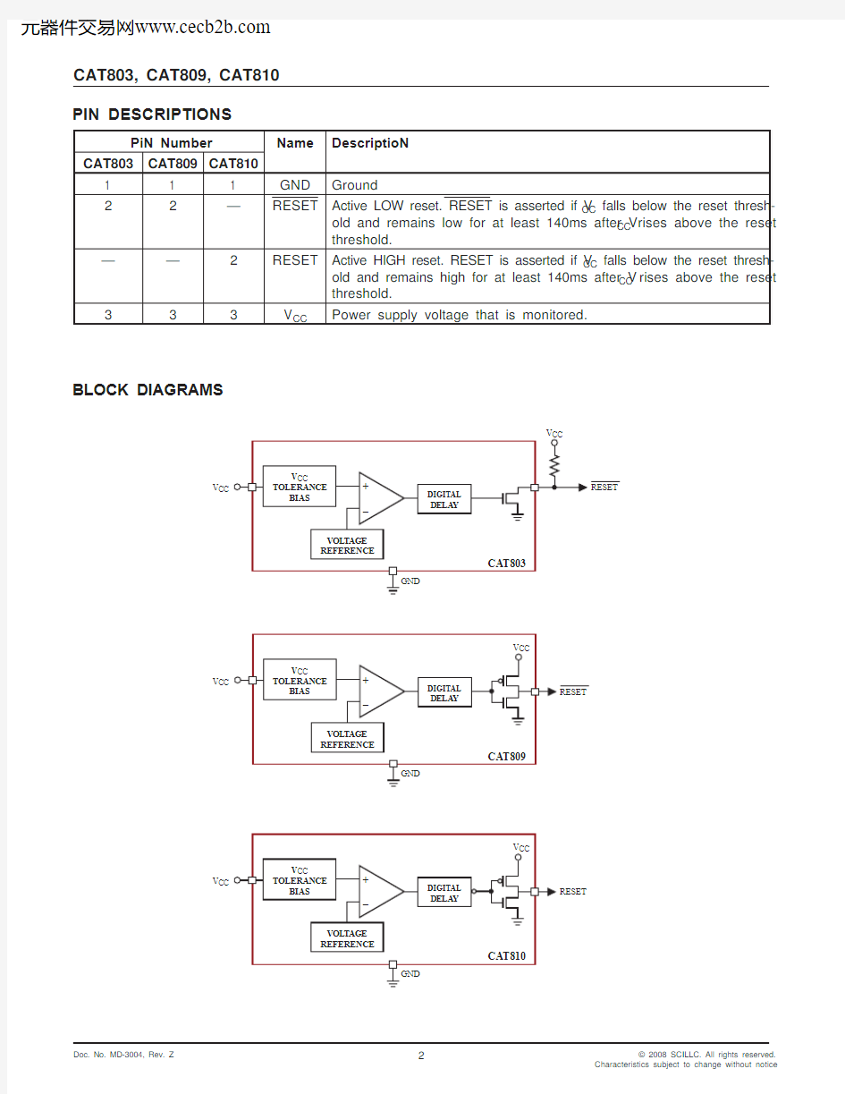
The CAT803, CAT809, and CAT8 0 are supervisory circuits that monitor power supplies in digital systems. The CAT803, CAT809, and CAT8 0 are direct replacements for the MAX803, MAX809 and MAX8 0 in applications operating over the industrial temperature range.These devices generate a reset signal, which is asserted while the power supply voltage is below a preset threshold level and for at least 40 ms after the power supply level has risen above that level. The underlying floating gate technology, AE 2(TM) used by Catalyst Semiconductor, makes it possible to offer any custom reset threshold value. Seven industry standard threshold levels are offered to support +5.0V, +3.3V, +3.0V and +2.5V systems.
The CAT803 has an open-drain RESET output (active LOW). The CAT803 requires a pull-up resistor on the reset output.
The CAT809 features a push-pull RESET output (active LOW) and the CAT8 0 features a push-pull RESET output (active HIGH).
Fast transients on the power supply are ignored and the output is guaranteed to be in the correct state at V cc levels as low as .0V.
The CAT803, CAT809, and CAT8 0 are available in both the compact 3-pin SOT-23 and SC-70 packages.
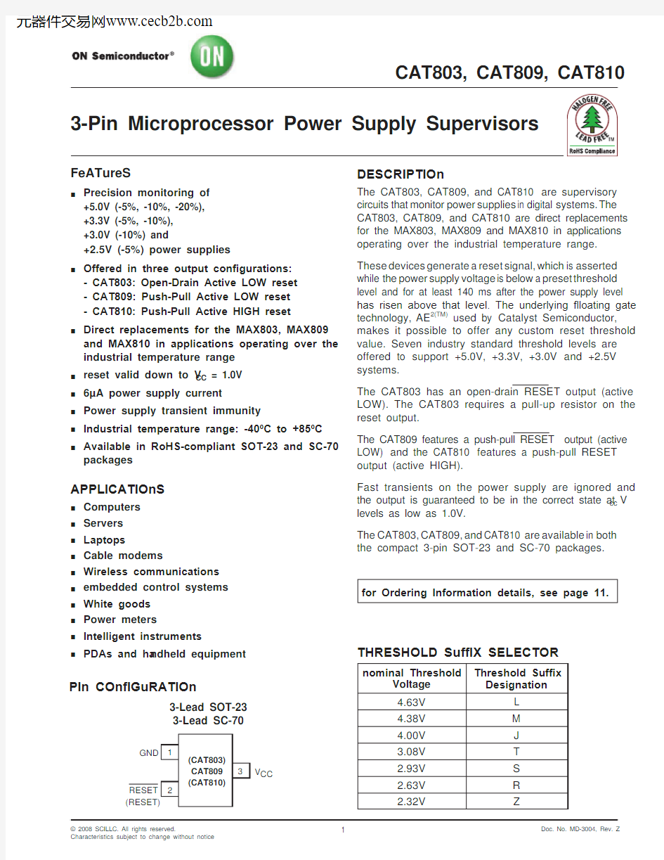
PIn COnfIGuRATIOn
(CAT803)CAT809(CAT810)
GND
RESET (RESET)
V CC
3-Lead SOT-23
3-Lead SC-70
1
23
THRESHOLD SuffIX SELECTOR
nominal Threshold Voltage Threshold Suffix
Designation
4.63V L 4.38V M 4.00V J 3.08V
T 2.93V S 2.63V R 2.32V
Z
for Ordering Information details, see page 11.
CAT803, CAT809, CAT8102
Doc. No. MD-3004, Rev. Z
? 2008 SCILLC. All rights reserved.
Characteristics subject to change without notice
V CC
V CC
RESET
V CC
PIn DESCRIPTIOnS
Pin number
name
Description
CAT803
CAT809CAT810
GND
Ground
2
2
—
RESET Active LOW reset. RESET is asserted if V CC falls below the reset thresh-old and remains low for at least 40ms after V CC rises above the reset threshold.——2
RESET Active HIGH reset. RESET is asserted if V CC falls below the reset thresh-old and remains high for at least 40ms after V CC rises above the reset threshold.333
V CC
Power supply voltage that is monitored.
BLOCK DIAGRAMS
CAT803, CAT809, CAT810
3
Doc. No. MD-3004, Rev. Z
? 2008 SCILLC. All rights reserved.
Characteristics subject to change without notice
ELECTRICAL CHARACTERISTICS
V CC = Full range, T A = -40oC to +85oC unless otherwise noted. Typical values at T A = +25oC and V CC = 5V for the L/M/J versions, V CC = 3.3V for the T/S versions, V CC = 3V for the R version and V CC = 2.5V for the Z version.Parameter Symbol
Conditions Min Typ
Max units V CC Range T A = 0oC to +70oC .0 5.5V
T A = -40oC to +85oC .2
5.5Supply Current I CC T A = -40oC to +85oC
V CC < 5.5V, J/L/M 820μA V CC < 3.6V, R/S/T/Z 6 5Reset Threshold Voltage
V TH L Threshold T A = +25oC 4.56 4.63 4.70V T A = -40oC to +85oC 4.50 4.75M Threshold T A = +25oC 4.3 4.38
4.45T A = -40oC to +85oC 4.25 4.50J Threshold T A = +25oC 3.93 4.00 4.06T A = -40oC to +85oC 3.89 4. 0T Threshold T A = +25oC 3.04 3.08 3. T A = -40oC to +85oC 3.00 3. 5S Threshold T A = +25oC 2.89 2.93 2.96T A = -40oC to +85oC 2.85 3.00R Threshold T A = +25oC 2.59 2.63 2.66T A = -40oC to +85oC 2.55 2.70Z Threshold
T A = +25oC 2.28 2.32 2.35T A = -40oC to +85oC
2.25
2.38
ABSOLuTE MAXIMuM RATInGS (1)Any pin with respect to ground -0.3V to +6.0V Input Current, V CC
20mA Output Current, RESET, RESET 20mA Rate of Rise, V CC
00V/μs Continuous Power Dissipation Derate 2.2mW/oC above 70oC (SC70) 75 mW Derate 4mW/oC above 70oC (SOT23)320 mW Operating Temperature Range -40oC to +85oC Storage Temperature Range -65oC to + 05oC Lead Soldering Temperature ( 0 sec)
300oC
note:
( ) Stresses above those listed under “Absolute Maximum Ratings” may cause permanent damage to the device. These are stress ratings only,
and functional operation of the device at these or any other conditions outside of those listed in the operational sections of this specification is not implied. Exposure to any absolute maximum rating for extended periods may affect device performance and reliability.
CAT803, CAT809, CAT810
4
Doc. No. MD-3004, Rev. Z
? 2008 SCILLC. All rights reserved.
Characteristics subject to change without notice
ELECTRICAL CHARACTERISTICS V CC = Full range, T A = -40oC to +85oC unless otherwise noted. Typical values at T A = +25oC and V CC = 5V for L/M/J versions, V CC = 3.3V for T/S versions, V CC = 3V for R version and V CC = 2.5V for Z version.(continued)
notes:
( ) Production testing done at T A = +25oC; limits over temperature guaranteed by design only.(2) Parameter
Symbol Conditions
Min
Typ (1)Max
units Reset Threshold Tempco 30ppm/oC V CC to Reset Delay (Note 2)T D V CC = V TH to (V TH - 00 mV)20μs Reset Active Timeout Period T R
T A = -40oC to +85oC
40
240
460ms
RESET Output Voltage Low (Open-drain active LOW, CAT803 and push-pull, active LOW, CAT809)V OL V CC = V TH min, I SINK = .2mA CAT803R/S/T/Z, CAT809R/S/T/Z 0.3V
V CC = V TH min, I SINK = 3.2mA CAT803J/L/M, CAT809J/L/M 0.4V CC > .0V, I SINK = 50μA 0.3
RESET Output Voltage High (Push-pull, active LOW, CAT809)
V OH V CC = V TH max, I SOURCE = 500μA CAT809R/S/T/Z
0.8 V CC V
V CC = V TH max, I SOURCE = 800μA CAT809J/L/M
V CC - .5
RESET Output Voltage Low (Push-pull, active HIGH, CAT8 0)
V OL V CC > V TH max, I SINK = .2mA CAT8 0R/S/T/Z
0.3V V CC > V TH max, I SINK = 3.2mA CAT8 0J/L/M 0.4
RESET Output Voltage High (Push-pull active HIGH, CAT8 0)
V OH .8V < V CC V TH min, I SOURCE = 50μA
0.8 V CC
V
CAT803, CAT809, CAT810
5
Doc. No. MD-3004, Rev. Z
? 2008 SCILLC. All rights reserved.
Characteristics subject to change without notice
TyPICAL OPERATInG CHARACTERISTICS
V CC = Full range, T A = -40oC to +85oC unless otherwise noted. Typical values at T A = +25oC and V CC = 5V for L/M/J versions, V CC =3.3V for T/S versions, V CC = 3V for R version and V CC = 2.5V for Z version.
SUPPLY CURRENT VS. TEMPERATURE
(NO LOAD, CAT8xxR/S/T/Z)12
1086420
-50 0 50 100 150
S U P P L Y C U R R E N T (μA )
TEMPERATURE (?C)
POWER-DOWN RESET DELAY VS. TEMPERATURE
(CAT8xxR/S/T/Z)1412108642
P O W E R -D O W N R E S E T D E L A Y (μS )
TEMPERATURE (?C)
POWER-UP RESET TIMEOUT
VS. TEMPERATURE
260
240220200180160
P O W E R -U P R E S E T T I M E O U T (m S )
TEMPERATURE (?C)NORMALIZED RESET THRESHOLD
VS. TEMPERATURE
1.0002
10.99980.99960.99940.99920.9990.9988
0 20 40 60 80 100 120
N O R M A L I Z E D T H R E S H O L D
TEMPERATURE (?C)
-50 0 50 100 150
-50 0 50 100 150
CAT803, CAT809, CAT8106
Doc. No. MD-3004, Rev. Z
? 2008 SCILLC. All rights reserved.
Characteristics subject to change without notice
0V
5V 0V
5V
RESET/OUT
RESET
V TH V CC
0V
5V DETAILED DESCRIPTIOnS
RESET TIMInG
The reset signal is asserted LOW for the CAT803/ CAT809 and HIGH for the CAT8 0 when the power supply voltage falls below the threshold trip voltage and remains asserted for at least 40ms after the power supply voltage has risen above the threshold.
figure 2. Maximum Transient Duration Without Causing a Reset Pulse vs. Reset Comparator Overdrive
T R A N S I E N T D U R A T I O N (μs )
V CC TRAnSIEnT RESPOnSE
The CAT803/CAT809/CAT8 0 protect μPs against brownout failure. Short duration transients of 4μsec or less and 00mV amplitude typically do not cause a false RESET.
Figure 2 shows the maximum pulse duration of negative-going V CC transients that do not cause a reset condition.
figure 1. Reset Timing Diagram
As the amplitude of the transient goes further below the threshold (increasing V TH - V CC ), the maximum pulse duration decreases. In this test, the V CC starts from an initial voltage of 0.5V above the threshold and drops below it by the amplitude of the overdrive voltage (V TH - V CC ).
CAT803, CAT809, CAT810
7
Doc. No. MD-3004, Rev. Z
? 2008 SCILLC. All rights reserved.
Characteristics subject to change without notice
VALID RESET WITH V CC unDER 1.0V
To ensure that the CAT809 RESET pin is in a known state when V CC is under 1.0V, a >10k? pull-down resistor between RESET pin and GND is recommended. For the CAT8 0, a pull-up resistor from RESET pin to V CC is needed.
Power Supply
Figure 3. reSeT Valid with V CC under 1.0V figure 4. RESET Valid with V CC under 1.1V
figure 5. Bi-directional Reset Pin Interfacing
Power Supply
BI-DIRECTIOnAL RESET PIn InTERfACInG The CAT809/8 0 can interface with μP/μC bi-directional reset pins by connecting a 4.7k? resistor in series with the CAT809/8 0 reset output and the μP/μC bi-directional reset pin.
CAT803, CAT809, CAT810
8
Doc. No. MD-3004, Rev. Z
? 2008 SCILLC. All rights reserved.
Characteristics subject to change without notice
CAT803 OPEn-DRAIn reSeT APPLICATIOn The CAT803 features an open-drain RESET output and therefore needs a pull-up resistor on the output for proper operation, as shown on Figure 6. An advantage of the open-drain output includes the ability to “wire AND” several outputs together to form an inexpensive logic circuit. It is also possible to have the pull-up resistor connected to a different supply which can be higher than the CAT803 V CC pin. The value of the pull-up resistor is not critical in most applications, typical values being between 5k? and 10k?.
Power Supply
figure 6. Typical CAT803 Open-Drain Circuit Configuration
CAT803, CAT809, CAT810
9
Doc. No. MD-3004, Rev. Z
? 2008 SCILLC. All rights reserved.
Characteristics subject to change without notice
PACKAGE OuTLInE DRAWInGS
SOT-23 3-Lead (TB)
notes:
( ) All dimensions are in millimeters. Angles in degrees.(2) Complies with JEDEC standard TO-236.
TOP VIEW
SIDE VIEW END VIEW
PACKAGE OUTLINE DRAWING
SOT-23 3-Lead (TP , TB)
Doc. No. SOT233-007-01
07/20/07
(1) All dimensions are in millimeters. Angles in degrees.(2) Complies with JEDEC TO-236.
SYMBOL MIN NOM MAX
A 0.89 1.12 A1 0.013 0.10 b 0.37 0.50
c 0.085 0.18 D 2.80 3.04 E 2.10 2.64 E1 1.20 1.40
e 0.95 BSC e1 1.90 BSC L 0.400 REF L1 0.540 REF
θ
0o
8o
for current Tape and Reel information, download the PDf file from: https://www.doczj.com/doc/4917946381.html,/documents/tapeandreel.pdf
CAT803, CAT809, CAT810
Doc. No. MD-3004, Rev. Z
? 2008 SCILLC. All rights reserved.
Characteristics subject to change without notice
SC-70 3-Lead (SD)
notes:
( ) All dimensions are in millimeters. Angles in degrees.(2) Complies with JEDEC standard MO-203.
for current Tape and Reel information, download the PDf file from: https://www.doczj.com/doc/4917946381.html,/documents/tapeandreel.pdf
TOP VIEW
SIDE VIEW
END VIEW
θPACKAGE OUTLINE DRAWING
SC-70 3-Lead (SB, SD)
Doc. No. SC703-046-01
01/31/08(1) All dimensions are in millimeters. Angles in degrees.(2) Complies with JEDEC MO-203.
SYMBOL MIN NOM MAX
A 0.80 1.10 A1 0.00 0.10 A2 0.80 0.90 1.00 b 0.15 0.30
c 0.08 0.22 D 1.80 2.00 2.20 E 1.80 2.10 2.40 E1 1.15 1.25 1.35 e 0.65 BSC L 0.26 0.36 0.46
L1 0.42 REF L2 0.15 BSC
θ 0° 8°
θ1
4°
10°
CAT803, CAT809, CAT810
Doc. No. MD-3004, Rev. Z
? 2008 SCILLC. All rights reserved.
Characteristics subject to change without notice
EXAMPLE Of ORDERInG InfORMATIOn
(2) (3) (4)
Prefix Device #
Suffix
TOP MARKInG
notes:
( ) All packages are RoHS-compliant (Lead-free, Halogen-free).
(2) The standard lead finish is NiPdAu. Contact factory for other lead finishes.
(3) The device used in the example above is a CAT809STBI-GT 0 (Push-Pull / Active Low Output, trip level of 2.85V to 3.00V NiPdAu, Tape
and Reel).
(4) For additional package and temperature options, please contact your nearest ON Semiconductor Sales office.
Device
(1)
SOT-23 PbSn Finish (2)
SOT-23 RoHS Matte Finish (2)SOT-23 RoHS
niPdAu Finish (2)(3)SC70 PbSn Finish (2)
SC70 RoHS
Matte Finish (2)
SC70 RoHS
niPdAu Finish (2)(3)
CAT803x N/A RPYM RNYM N/A RP__RN__CAT809x PAYM PBYM NRYM PA__PB__NR__CAT8 0x
PCYM
PDYM
NSYM
PC__
PD__
NS__
notes:
( ) All theshold trip level options have the same marking.
(2) The “YM” in the SOT-23 package marking indicates the Year and Month of roduction and the “_” in the SC70 package marking indicates the
assembly location.
(3) All NiPdAu devices will be marked to indicate product type and package. Threshold and full part numbers will be provided on box and reel
labels as well as all Shipping documents.
CAT803, CAT809, CAT810 2
Doc. No. MD-3004, Rev. Z
? 2008 SCILLC. All rights reserved.
Characteristics subject to change without notice
note:
( ) Contact Factory for availability.
CAT803LSDI ( )CAT803LSDI-G CAT809LSDI ( )CAT809LSDI-G CAT8 0LSDI ( )CAT8 0LSDI-G CAT803MSDI ( )CAT803MSDI-G CAT809MSDI ( )CAT809MSDI-G CAT8 0MSDI ( )CAT8 0MSDI-G CAT803JSDI ( )CAT803JSDI-G CAT809JSDI ( )CAT809JSDI-G CAT8 0JSDI ( )CAT8 0JSDI-G CAT803TSDI ( )CAT803TSDI-G CAT809TSDI ( )CAT809TSDI-G CAT8 0TSDI ( )CAT8 0TSDI-G CAT803SSDI ( )CAT803SSDI-G CAT809SSDI ( )CAT809SSDI-G CAT8 0SSDI ( )CAT8 0SSDI-G CAT803RSDI ( )CAT803RSDI-G CAT809RSDI ( )CAT809RSDI-G CAT8 0RSDI ( )CAT8 0RSDI-G CAT803ZSDI ( )CAT803ZSDI-G CAT809ZSDI ( )CAT809ZSDI-G CAT8 0ZSDI ( )CAT8 0ZSDI-G CAT803LTBI ( )CAT803LTBI-G CAT809LTBI ( )CAT809LTBI-G CAT8 0LTBI ( )CAT8 0LTBI-G CAT803MTBI ( )CAT803MTBI-G CAT809MTBI ( )CAT809MTBI-G CAT8 0MTBI ( )CAT8 0MTBI-G CAT803JTBI ( )CAT803JTBI-G CAT809JTBI ( )CAT809JTBI-G CAT8 0JTBI ( )CAT8 0JTBI-G CAT803TTBI ( )CAT803TTBI-G CAT809TTBI ( )CAT809TTBI-G CAT8 0TTBI ( )CAT8 0TTBI-G CAT803STBI ( )CAT803STBI-G CAT809STBI ( )CAT809STBI-G CAT8 0STBI ( )CAT8 0STBI-G CAT803RTBI ( )CAT803RTBI-G CAT809RTBI ( )CAT809RTBI-G CAT8 0RTBI ( )CAT8 0RTBI-G CAT803ZTBI ( )
CAT803ZTBI-G
CAT809ZTBI ( )
CAT809ZTBI-G
CAT8 0ZTBI ( )
CAT8 0ZTBI-G
ORDERInG PART nuMBER
CAT803, CAT809, CAT810
3
Doc. No. MD-3004, Rev. Z
? 2008 SCILLC. All rights reserved.
Characteristics subject to change without notice
REVISIOn HISTORy
Date rev.Description
29-Oct-03N Updated VCC Transient Response text and Figure 230-Oct-03O Updated Power Up Reset Timeout vs. Temperature curve 3-Oct-04
P
Corrected temperature range Updated Description
Updated Ordering Information
Updated Absolute Maximum Ratings Updated Electrical Characteristics 23-Mar-04Q
Updated Description
Updated Ordering Information
Updated Absolute Maximum Ratings Updated Electrical Characteristics
Updated Typical Operating Characteristics Updated Package Information
25-Mar-04R
Changed Preliminary designation to Final
Updated Max Reset Active Timeout Period in Electrical Characteristics Updated package drawings 5-Oct-04S Updated top marking table 28-Feb-05
T
Updated Features
Updated Ordering Information Updated Top Marking
7-Feb-06Q Updated Typical Operating Characteristics
0-Aug-06
U
Updated Features Updated Description
Updated Max Reset Active Timeout Period in Electrical Characteristics Updated Figure
Updated Package Information Correct Revision Number 7-Oct-06V
Updated Top Marking
Updated Detailed Description Adding CAT803
2-Feb-07W
Updated Electrical Characteristics Updated Figure
Updated Ordering Information 20-Mar-07X Updated Detailed Descriptions
3 -Jan-08
Y
Added MD- to Document Number Added Block Diagrams
Updated Package Outline Drawings
Updated Example of Ordering Information Updated Ordering Part Number
05-Nov-08Z
Change logo and fine print to ON Semiconductor
ON Semiconductor and are registered trademarks of Semiconductor Components Industries, LLC (SCILLC). SCILLC reserves the right to make changes without further notice to any products herein. SCILLC makes no warranty, representation or guarantee regarding the suitability of its products for any particular purpose, nor does SCILLC assume any liability arising out of the application or use of any product or circuit, and specifically disclaims any and all liability, including without limitation special, consequential or incidental damages. “Typical” parameters which may be provided in SCILLC data sheets and/or specifications can and do vary in different applications and actual performance may vary over time. All operating parameters, including “Typicals” must be validated for each customer application by customer’s technical experts. SCILLC does not convey any license under its patent rights nor the rights of others. SCILLC products are not designed, intended, or authorized for use as components in systems intended for surgical implant into the body, or other applications intended to support or sustain life, or for any other application in which the failure of the SCILLC product could create a situation where personal injury or death may occur. Should Buyer purchase or use SCILLC products for any such unintended or unauthorized application, Buyer shall indemnify and hold SCILLC and its officers, employees, subsidiaries, affiliates, and distributors harmless against all claims, costs, damages, and expenses, and reasonable attorney fees arising out of, directly or indirectly, any claim of personal injury or death associated with such unintended or unauthorized use, even if such claim alleges that SCILLC was negligent regarding the design or manufacture of the part. SCILLC is an Equal Opportunity/Affirmative Action Employer. This literature is subject to all applicable copyright laws and is not for resale in any manner.
PuBLICATIOn ORDERInG InfORMATIOn
LITERATuRE fuLfILLMEnT:
Literature Distribution Center for On Semiconductor
P.O. Box 5 63, Denver, Colorado 802 7 USA
Phone: 303-675-2 75 or 800-344-3860 Toll Free USA/Canada fax: 303-675-2 76 or 800-344-3867 Toll Free USA/Canada Email: orderlit@https://www.doczj.com/doc/4917946381.html, n. American Technical Support: 800-282-9855 Toll Free
USA/Canada
Europe, Middle East and Africa Technical Support:
Phone: 42 33 790 29 0
Japan Customer focus Center:
Phone: 8 -3-5773-3850
On Semiconductor Website: https://www.doczj.com/doc/4917946381.html,
Order Literature: https://www.doczj.com/doc/4917946381.html,/orderlit
For additional information, please contact your local
Sales Representative