Complementary 20-V (D-S) Low-Threshold MOSFET
PRODUCT SUMMARY
Channel
V DS (V)
r DS(on) (W )
I D (mA)
2.0 @ V GS = 4.5 V 250N-Channel
20
2.5 @ V GS = 2.5 V 150P Channel 20
3.8 @ V GS = ?
4.5 V ?180P-Channel ?
5.0 @ V GS = ?2.5 V
?100
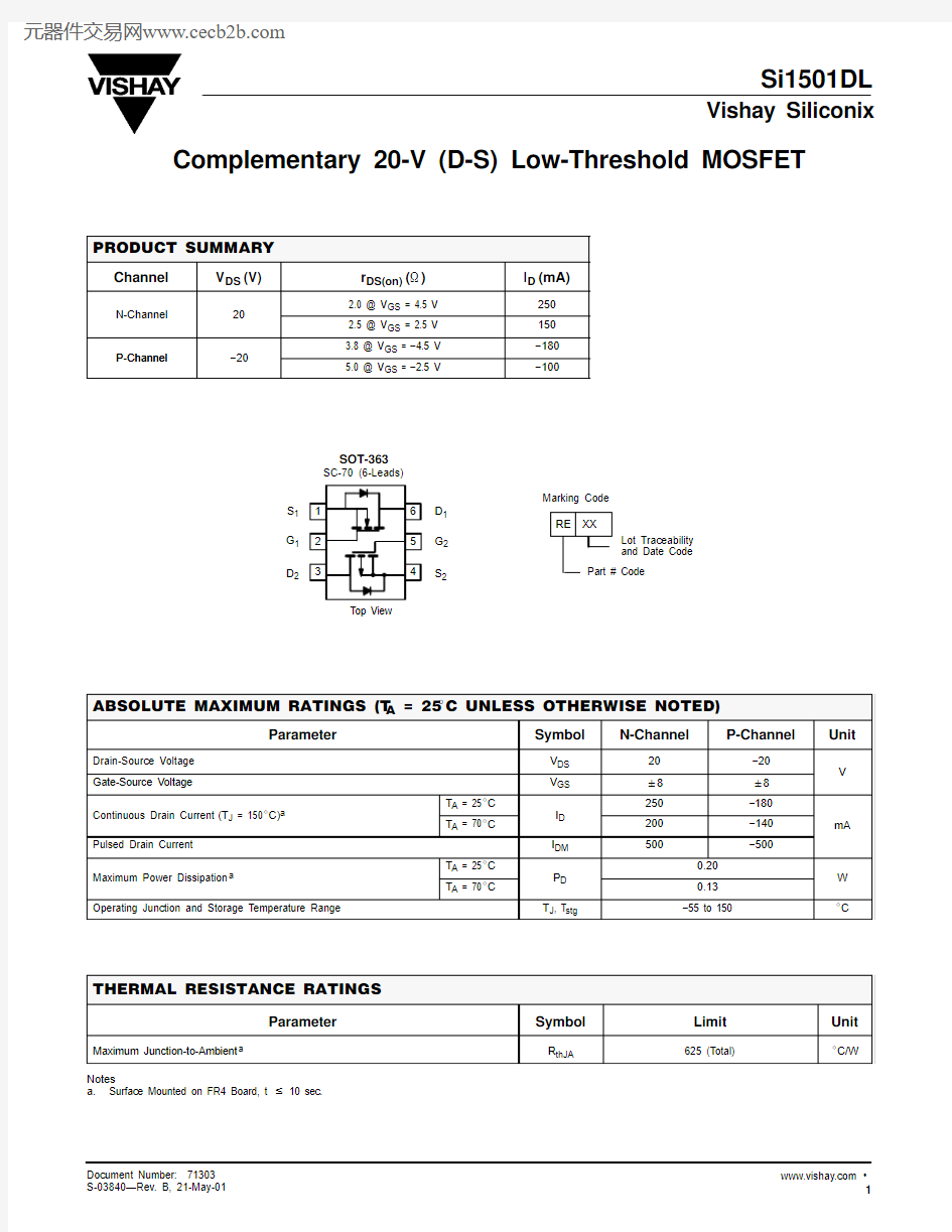
SOT-363
SC-70 (6-Leads)
S 1G 1D 2
D 1G 2S 2
Top View
Marking Code
RE
XX
Lot Traceability
and Date Code
Part # Code
Y Y
ABSOLUTE MAXIMUM RATINGS (T A = 25_C UNLESS OTHERWISE NOTED)
Parameter
Symbol
N-Channel
P-Channel
Unit
Drain-Source Voltage V DS 20?20Gate-Source Voltage
V GS "8"8V
T A = 25_C 250?180Continuous Drain Current (T J = 150_C)a T A = 70_C
I D 200?140mA
Pulsed Drain Current I DM 500
?500
Maximum Power Dissipation T A = 25_C 0.20a
T A = 70_C P D 0.13
W Operating Junction and Storage Temperature Range
T J , T stg
?55 to 150
_C
THERMAL RESISTANCE RATINGS
Parameter
Symbol
Limit
Unit
Maximum Junction-to-Ambient a
R thJA
625 (Total)
_C/W
Notes
a.Surface Mounted on FR4 Board, t v 10 sec.
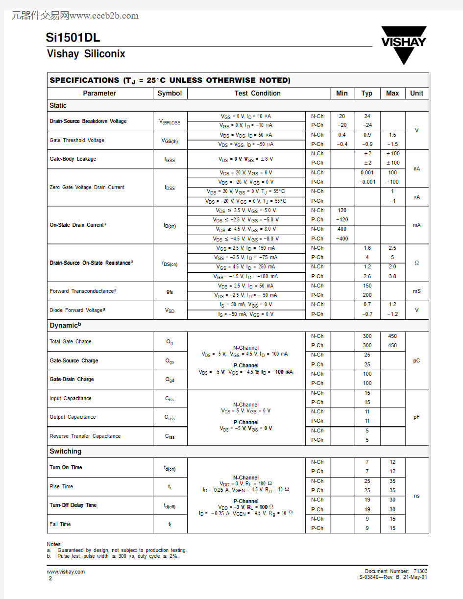
SPECIFICATIONS (T J = 25_C UNLESS OTHERWISE NOTED)
Parameter
Symbol Test Condition Min Typ Max Unit
Static
Drain Source Breakdown Voltage V GS = 0 V, I D = 10 m A N-Ch 2024Drain-Source Breakdown Voltage V (BR)DSS V GS = 0 V, I D = ?10 m A P-Ch ?20?24GS(h)V DS = V GS , I D = 50 m A N-Ch 0.40.9 1.5V
Gate Threshold Voltage V GS(th)V DS = V GS , I D = ?50 m A P-Ch ?0.4
?0.9?1.5Gate Body Leakage = 0 V V N-Ch "2"100Gate-Body Leakage
I GSS
V DS = 0 V, V GS = "8 V P-Ch "2"100V DS = 20 V, V GS = 0 V
N-Ch 0.001100nA V DS = ?20 V, V GS = 0 V P-Ch ?0.001
?100Zero Gate Voltage Drain Current
I DSS
V DS = 20 V, V GS = 0 V, T J = 55_C N-Ch 1V DS = ?20 V, V GS = 0 V, T J = 55_C
P-Ch ?1
m A V DS w 2.5 V, V GS = 5.0 V
N-Ch 120On State Drain Current D()
V DS v ?2.5 V, V GS = ?5.0 V P-Ch ?120On-State Drain Current a
I D(on)V DS w 4.5 V, V GS = 8.0 V N-Ch 400mA
V DS v ?4.5 V, V GS = ?8.0 V P-Ch ?400
V GS = 2.5 V, I D = 150 mA
N-Ch 1.6 2.5Drain Source On State Resistance DS()
V GS = ?2.5 V, I D = ?75 mA P-Ch 45Drain-Source On-State Resistance a
r DS(on)V GS = 4.5 V, I D = 250 mA N-Ch 1.2 2.0W V GS = ?4.5 V, I D = ?180 mA
P-Ch 2.6 3.8
Forward Transconductance f V DS = 2.5 V, I D = 50 mA N-Ch 150a g fs V DS = ?2.5 V, I D = ? 50 mA P-Ch 200mS I S = 50 mA, V GS = 0 V N-Ch 0.7 1.2Diode Forward Voltage a
V SD
I S = ?50 mA, V GS = 0 V
P-Ch
?0.7
?1.2V Dynamic b
N-Ch
300450Total Gate Charge Q g N-Channel
P-Ch 300450
Gate Source Charge V DS = 5 V, V GS = 4.5 V, I D = 100 mA N-Ch 25Gate-Source Charge Q gs P-Channel V V I 100 A P-Ch 25pC
Gate Drain Charge d P Channel
V DS = ?5 V, V GS = ?4.5 V, I D = ?100 mA
N-Ch 100Gate-Drain Charge Q gd P-Ch 100i N-Ch
15Input Capacitance C iss N-Channel
P-Ch 15V DS = 5 V, V GS = 0 V N-Ch 11Output Capacitance
C oss P-Channel V V 0 V
P-Ch 11pF
P Channel V DS = ?5 V, V GS = 0 V N-Ch 5Reverse Transfer Capacitance
C rss
P-Ch
5
Switching
Turn On Time d()N-Ch 712Turn-On Time t d(on)N Channel
P-Ch 712N-Channel N-Ch 2535Rise Time
t r V DD = 3 V, R L = 100 W
I D = 0.25 A, V GEN = 4.5 V, R = 10 W P-Ch 2535Turn Off Delay Time d(ff)g P-Channel 3 V R 100 W
N-Ch 1930ns
Turn-Off Delay Time t d(off)P Channel V DD = ?3 V, R L = 100 I 4.5 V, R W
P-Ch 1930D = -0.25 A, V GEN = ?g = 10 N-Ch 915Fall Time
t f
P-Ch
9
15
Notes
a.Guaranteed by design, not subject to production testing.
b.Pulse test; pulse width v 300 m s, duty cycle v 2%.
0.00.5
1.0 1.5
2.0 2.5
3.0
1
2
3
4
5
6
7
01234
01234
2
4
6
8
10
0100200300400500600
0.6
0.8
1.0
1.2
1.4
1.6
?50?250255075100125150 Gate Charge
On-Resistance vs. Drain Current
V DS? Drain-to-Source Voltage (V)V GS? Gate-to-Source Voltage (V)
?
G
a
t
e
-
t
o
-
S
o
u
r
c
e
V
o
l
t
a
g
e
(
V
)
Q g? Total Gate Charge (pC)
V DS? Drain-to-Source Voltage (V)
C
?
C
a
p
a
c
i
t
a
n
c
e
(
p
F
)
V
G
S
?
O
n
-
R
e
s
i
s
t
a
n
c
e
(
r
D
S
(
o
n
)
W
)
I D? Drain Current (A)
Capacitance
T J? Junction Temperature (_C)
(
N
o
r
m
a
l
i
z
e
d
)
?
O
n
-
R
e
s
i
s
t
a
n
c
e
(
r
D
S
(
o
n
)
W
)
10
20
30
40
50
048121620
TYPICAL CHARACTERISTICS (25_C UNLESS NOTED)
N-CHANNEL
?0.4
?0.3?0.2?0.1?0.00.1
0.2?50
?250
255075100125150
1.2
02
4
68
2
4
6
8
10
0.001
30.00
0.3
0.9
Threshold Voltage
V a r i a n c e (V )
V G S (t h )T J ? Temperature (_C)
Source-Drain Diode Forward Voltage
On-Resistance vs. Gate-to-Source Voltage
? O n -R e s i s t a n c e (r D S (o n )W )
V SD ? Source-to-Drain Voltage (V)
V GS ? Gate-to-Source Voltage (V)
? S o u r c e C u r r e n t (A )
I S 0.1
0.01
1
0.6
0.0
0.5
1.0
1.5
2.0
2.5
3.0
02
4
6
8
0.0
0.5
1.0
1.5
2.0
2.5
3.0
1
2
3
4
0246
810
100
200
300
400
500
600
0.60.8
1.0
1.2
1.4
1.6
?50
?250255075100125150
9
18
27
36
45
3
6
9
12
Gate Charge
On-Resistance vs. Drain Current
V DS ? Drain-to-Source Voltage (V)
V GS ? Gate-to-Source Voltage (V)
? G a t e -t o -S o u r c e V o l t a g e (V )
Q g ? Total Gate Charge (pC)
V DS ? Drain-to-Source Voltage (V)
C ? C a p a c i t a n c e (p F )
V G S ? O n -R e s i s t a n c e (r D S (o n )W )
I D ? Drain Current (A)Capacitance
On-Resistance vs. Junction Temperature
T J ? Junction Temperature (_C)
(N o r m a l i z e d )
? O n -R e s i s t a n c e (r D S (o n )W )
?0.2
?0.1
0.0
0.1
0.2
0.3
?50
?250255075100125150
1.5
1.0
1.5
2.0 2.5
3.0 3.5
4.0 4.5
0.00
0.5
01
Threshold Voltage
V a r i a n c e (V )
V G S (t h )T J ? Temperature (_C)
V SD ? Source-to-Drain Voltage (V)
V GS ? Gate-to-Source Voltage (V)