https://www.doczj.com/doc/4d9415491.html,
FEATURES
APPLICATIONS
DESCRIPTION
bq20z90-V110
SLUS743–NOVEMBER2006 SBS1.1-COMPLIANT GAS GAUGE ENABLED WITH IMPEDANCE TRACK?
TECHNOLOGY FOR USE WITH THE bq29330
Improved System Interaction
?Patented Impedance Track?Technology?Optional Pulse Charging Feature for Improved
Accurately Measures Available Charge in Charge Times
Li-Ion and Li-Polymer Batteries?Drives3-,4-or5-Segment LED Display for ?Better than1%Error Over Lifetime of the Remaining Capacity Indication
Battery?Supports SHA-1Authentication
?Instant Accuracy–No Learning Cycle?Lifetime Data Logging
Required?30-Pin TSSOP(DBT)
?Automatically adjusts for battery aging,
battery self discharge and temperature
inefficiencies?Notebook PCs
?Supports the Smart Battery Specification SBS?Medical and Test Equipment
V1.1?Portable Instrumentation
?Works With the TI bq29330Analog Front-End
(AFE)Protection IC to Provide Complete Pack
Electronics Solution
The bq20z90-V110SBS-compliant gas gauge IC,?Full Array of Programmable Voltage,Current,incorporating patented Impedance Track?
and Temperature Protection Features technology,is designed for battery-pack or in-system
installation.The bq20z90-V110measures and ?Integrated Time Base Removes Need for
maintains an accurate record of available charge in External Crystal with Optional Crystal Input
Li-ion or Li-polymer batteries using its integrated ?Electronics for7.2-V,10.8-V or14.4-V Battery high-performance analog peripherals.The
Packs With50%Fewer External Components bq20z90-V110monitors capacity change,battery ?Based on a Powerful Low-Power RISC CPU impedance,open-circuit voltage,and other critical Core With High-Performance Peripherals parameters of the battery pack,and reports the
information to the system host controller over a ?Integrated Field Programmable FLASH
serial-communication bus.It is designed to work with Memory Eliminates the Need for External
the bq29330analog front-end(AFE)protection IC to Configuration Memory
maximize functionality and safety,and minimize ?Measures Charge Flow Using a component count and cost in smart battery circuits.
High-Resolution,16-Bit Integrating
The Impedance Track technology continuously Delta-Sigma Converter
analyzes the battery impedance,resulting in superior –Better Than0.65nVh of Resolution gas-gauging accuracy.This enables remaining
capacity to be calculated with discharge rate,–Self-Calibrating
temperature,and cell aging all accounted for during ?Uses16-Bit Delta-Sigma Converter for
each stage of every cycle.
Accurate Voltage and Temperature
Measurements
?Extensive Data Reporting Options For
Please be aware that an important notice concerning availability,standard warranty,and use in critical applications of Texas
Instruments semiconductor products and disclaimers thereto appears at the end of this data sheet.
IMPEDANCE TRACK is a trademark of Texas Instruments.
PRODUCTION DATA information is current as of publication date.Copyright?2006,Texas Instruments Incorporated Products conform to specifications per the terms of the Texas
Instruments standard warranty.Production processing does not
necessarily include testing of all parameters.
https://www.doczj.com/doc/4d9415491.html,
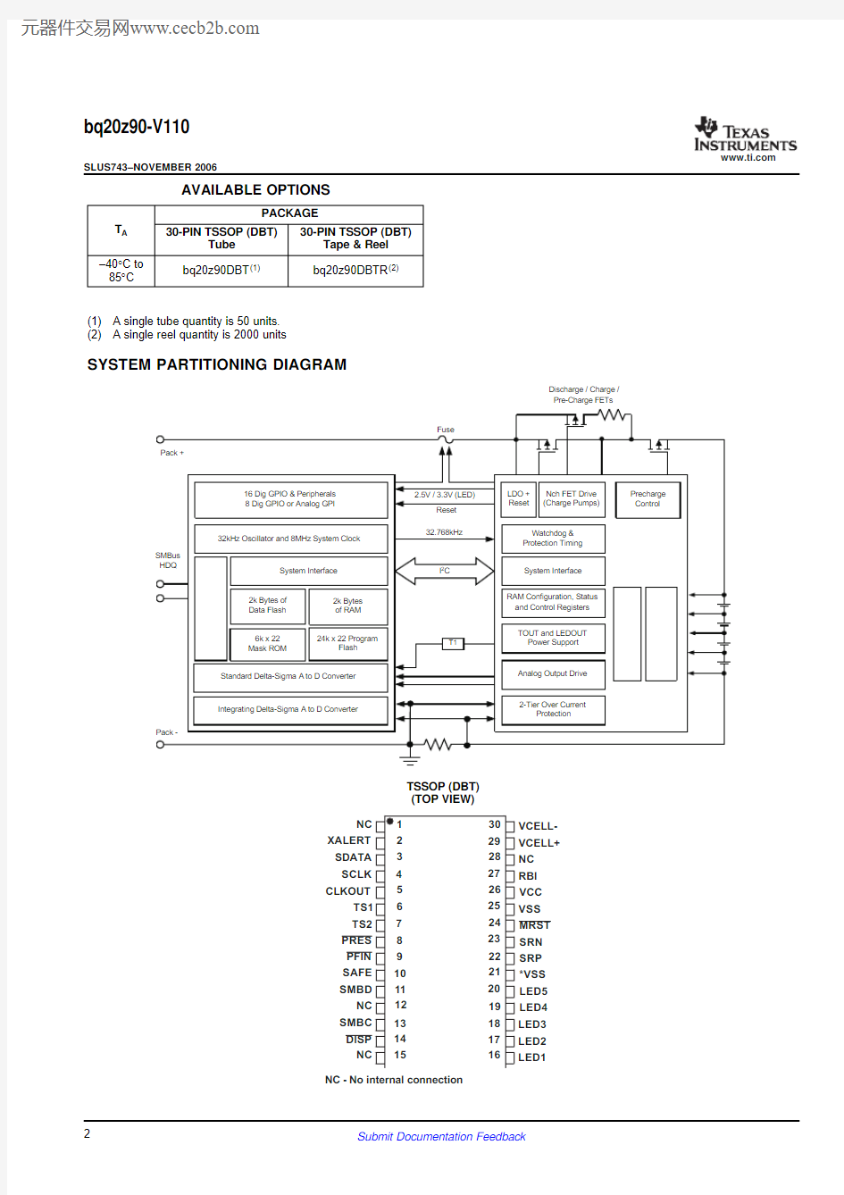
SYSTEM PARTITIONING DIAGRAM
Discharge / Charge /Pre-Charge FETs
VCC MRST SRN LED4LED5*VSS SRP NC - No internal connection
bq20z90-V110
SLUS743–NOVEMBER 2006
AVAILABLE OPTIONS
PACKAGE
T A 30-PIN TSSOP (DBT)
30-PIN TSSOP (DBT)
Tube Tape &Reel –40°C to bq20z90DBT (1)
bq20z90DBTR (2)
85°C
(1)A single tube quantity is 50units.(2)A single reel quantity is 2000units
TSSOP (DBT)(TOP VIEW)
2
Submit Documentation Feedback
https://www.doczj.com/doc/4d9415491.html,
bq20z90-V110
SLUS743–NOVEMBER2006 TERMINAL FUNCTIONS
TERMINAL
I/O(1)DESCRIPTION
https://www.doczj.com/doc/4d9415491.html,
1NC–Not used—leave floating
2XALERT I Input from bq29330XALERT output.
3SDATA I/O Data transfer to and from bq29330
4SCLK I/O Communication clock to the bq29330
5CLKOUT O32.768-kHz output for the bq29330.This pin should be directly connected to the AFE.
6TS1I1st Thermistor voltage input connection to monitor temperature
7TS2I2nd Thermistor voltage input connection to monitor temperature
8PRES I Active low input to sense system insertion and typically requires additional ESD protection
Active low input to detect secondary protector output status and allows the bq20z90-V110to report 9PFIN I
the status of the2nd level protection output
10SAFE O Active high output to enforce additional level of safety protection;e.g.,fuse blow.
11SMBD I/OD SMBus data open-drain bidirectional pin used to transfer address and data to and from the bq20z90 12NC–Not used—leave floating
13SMBC I/OD SMBus clock open-drain bidirectional pin used to clock the data transfer to and from the bq20z90
Display control for the LEDs.This pin is typically connected to bq29330REG via a100-k?resistor 14DISP I
and a push-button switch to VSS.
15NC–Not used—leave floating
16LED1O LED1display segment that drives an external LED depending on the firmware configuration
17LED2O LED2display segment that drives an external LED depending on the firmware configuration
18LED3O LED3display segment that drives an external LED depending on the firmware configuration
19LED4O LED4display segment that drives an external LED depending on the firmware configuration
20LED5O LED5display segment that drives an external LED depending on the firmware configuration
21VSS–Connected I/O pin to VSS
Connections to the top of a small-value sense resistor to monitor the battery charge-and 22SRP IA
discharge-current flow
Connections to the bottom of a small-value sense resistor to monitor the battery charge-and 23SRN IA
discharge-current flow
Master reset input that forces the device into reset when held low.Must be held high for normal 24MRST I
operation
25VSS P Negative Supply Voltage
26VCC P Positive Supply Voltage
Backup power to the bq20z90-V110data registers during periods of low operating voltage.RBI 27RBI P
accepts a storage capacitor or a battery input.
28NC–Not used—leave floating
29VCELL+I Input from bq29330used to read a scaled value of individual cell voltages
30VCELL-I Input from bq29330used to read a scaled value of individual cell voltages
(1)I=Input,IA=Analog input,I/O=Input/output,I/OD=Input/Open-drain output,O=Output,OA=Analog output,P=Power
3
Submit Documentation Feedback
https://www.doczj.com/doc/4d9415491.html,
ABSOLUTE MAXIMUM RATINGS
ELECTRICAL CHARACTERISTICS
bq20z90-V110
SLUS743–NOVEMBER 2006
over operating free-air temperature range (unless otherwise noted)(1)
RANGE
V CC relative to V SS Supply voltage range –0.3V to 2.75V V (IOD)relative to V SS Open-drain I/O pins
–0.3V to 6V V I relative to V SS Input voltage range to all other pins –0.3V to V CC +0.3V
T A Operating free-air temperature range –40°C to 85°C T stg Storage temperature range
–65°C to 150°C
(1)
Stresses beyond those listed under absolute maximum ratings may cause permanent damage to the device.These are stress ratings only,and functional operation of the device at these or any other conditions beyond those indicated under recommended operating conditions is not implied.Exposure to absolute-maximum-rated conditions for extended periods may affect device reliability.
V CC =2.4V to 2.6V,T A =–40°C to 85°C (unless otherwise noted)
PARAMETER
TEST CONDITIONS
MIN TYP MAX UNIT V CC Supply voltage
2.4
2.5 2.6
V
No flash programming
400(1)I CC
Operating mode current
μA
bq20z90-V110+475bq29330Sleep mode
8(1)I (SLP)Low-power storage mode current
μA bq20z90-V110+51
bq29330Output voltage low SMBC,SMBD,SDATA,SCLK,SAFE I OL =0.5mA 0.4V V OL LED1–LED5
I OL =10mA 0.4
V V OH Output high voltage,SMBC,SMBD,SDATA,SCLK,SAFE I OH =–1mA
V CC –0.5
V V IL
Input voltage low SMBC,SMBD,SDATA,SCLK,XALERT,–0.30.8V PRES,PFIN DISP
–0.30.8V V IH
Input voltage high SMBC,SMBD,SDATA,SCLK,XALERT,26
V PRES,PFIN DISP
2
V CC +0.3
V C IN
Input capacitance
5
pF V (AI1)Input voltage range VCELL+,VCELL-,TS1,TS2-0.20.8XV CC
V V (AI2)Input voltage range SR1,SR2
–0.20
0.20Z (AI2)Input impedance VCELL+,VCELL-,TS1,TS20V–1V 8M ?Z (AI1)Input impedance SR1,SR20V–1V
2.5
M ?(1)
This value does not include the bq29330
4
Submit Documentation Feedback
https://www.doczj.com/doc/4d9415491.html,
POWER-ON
RESET
1.76
1.77
1.78
1.79
1.8
1.81
-40
-20020406080
T - Free-Air Temperature - °C
A P o w e r -O n R e s e t N e g a t i v e -G o i n g V o l t a g e - V
POWER ON RESET BEHAVIOR
FREE-AIR TEMPERATURE
VS
INTEGRATING ADC (Coulomb Counter)CHARACTERISTICS
OSCILLATOR
bq20z90-V110
SLUS743–NOVEMBER 2006
V CC =2.4V to 2.6V,T A =–40°C to 85°C (unless otherwise noted)
PARAMETER
TEST CONDITIONS
MIN TYP MAX UNIT V IT–Negative-going voltage input 1.7 1.8 1.9V V HYS
Power-on reset hysteresis
50
125
200
mV
V CC =2.4V to 2.6V,T A =–40°C to 85°C (unless otherwise noted)
PARAMETER
TEST CONDITIONS
MIN TYP
MAX UNIT V (SR)Input voltage range,V (SRN)and V (SRP)V (SR)=V(SRN)–V(SRP)
–0.2
0.2
V V (SROS)Input offset
10μV
INL
Integral nonlinearity error
0.007%
0.034%V CC =2.4V to 2.6V,T A =–40°C to 85°C (unless otherwise noted)
PARAMETER
TEST CONDITIONS
MIN
TYP
MAX
UNIT
HIGH FREQUENCY OSCILLATOR f (OSC)Operating Frequency 4.194MHz
-3%0.25%
3%f (EIO)Frequency Error (1)(2)T A =20°C to 70°C
-2%0.25%
2%t (SXO)Start-up Time (3)
2.5
5
ms LOW FREQUENCY OSCILLATOR f (LOSC)Operating Frequency 32.768
KHz
-2.5%0.25% 2.5%f (LEIO)Frequency Error (2)(4)
T A =20°C to 70°C
-1.5%0.25%
1.5%
(1)The frequency error is measured from 4.194MHz.
(2)The frequency drift is included and measured from the trimmed frequency at V CC =2.5V,T A =25°C.
(3)The start-up time is defined as the time it takes for the oscillator output frequency to be within 1%of the specified frequency.(4)The frequency error is measured from 32.768kHz.
5
Submit Documentation Feedback
https://www.doczj.com/doc/4d9415491.html,
DATA FLASH MEMORY CHARACTERISTICS
REGISTER BACKUP
bq20z90-V110
SLUS743–NOVEMBER 2006
OSCILLATOR (continued)
V CC =2.4V to 2.6V,T A =–40°C to 85°C (unless otherwise noted)
PARAMETER
TEST CONDITIONS MIN TYP MAX UNIT t (LSXO)Start-up time (5)
500
μs
(5)
The start-up time is defined as the time it takes for the oscillator output frequency to be ±3%.
V CC =2.4V to 2.6V,T A =–40°C to 85°C (unless otherwise noted)
PARAMETER
TEST CONDITIONS MIN TYP MAX UNIT t DR
Data retention
See (1)10Years Flash programming write-cycles
See (1)20,000
Cycles
t (WORDPROG)Word programming time See (1)2
ms I (DDdPROG)Flash-write supply current
See
(1)
5
10
mA
(1)
Assured by design.Not production tested
V CC =2.4V to 2.6V,T A =–40°C to 85°C (unless otherwise noted)
PARAMETER
TEST CONDITIONS
MIN
TYP
MAX UNIT I (RB)
RB data-retention input current
V (RB)>V (RBMIN),V CC V (RB)>V (RBMIN),V CC 160 to 50°C V (RB)RB data-retention voltage (1) 1.7 V (1) Specified by design.Not production tested. 6 Submit Documentation Feedback https://www.doczj.com/doc/4d9415491.html, SMBus TIMING SPECIFICATIONS bq20z90-V110 SLUS743–NOVEMBER 2006 V CC =2.4V to 2.6V,T A =–40°C to 85°C (unless otherwise noted) PARAMETER TEST CONDITIONS MIN TYP MAX UNIT f SMB SMBus operating frequency Slave mode,SMBC 50%duty cycle 10 100 kHz f MAS SMBus master clock frequency Master mode,no clock low slave extend 51.2 t BUF Bus free time between start and stop 4.7t HD:STA Hold time after (repeated)start 4μs t SU:STA Repeated start setup time 4.7t SU:STO Stop setup time 4 Receive mode 0t HD:DAT Data hold time Transmit mode 300ns t SU:DAT Data setup time 250t TIMEOUT Error signal/detect See (1) 2535 ms t LOW Clock low period 4.7μs t HIGH Clock high period See (2)4 50t LOW:SEXT Cumulative clock low slave extend time See (3)25ms t LOW:MEXT Cumulative clock low master extend time See (4) 10t F Clock/data fall time (V ILMAX –0.15V)to (V IHMIN +0.15V)300ns t R Clock/data rise time 0.9VCC to (VILMAX –0.15V) 1000(1)The bq20z90-V110times out when any clock low exceeds t TIMEOUT . (2)t HIGH:MAX .is minimum bus idle time.SMBC =1for t >50μs causes reset of any transaction involving the bq20z90-V110that is in progress. (3)t LOW:SEXT is the cumulative time a slave device is allowed to extend the clock cycles in one message from initial start to the stop.(4) t LOW:MEXT is the cumulative time a master device is allowed to extend the clock cycles in one message from initial start to the stop. SMBus TIMING DIAGRAM 7 Submit Documentation Feedback https://www.doczj.com/doc/4d9415491.html, FEATURE SET Primary (1st Level)Safety Features Secondary (2nd Level)Safety Features Charge Control Features Gas Gauging bq20z90-V110 SLUS743–NOVEMBER 2006 The bq20z90-V110supports a wide range of battery and system protection features that can easily be configured.The primary safety features include:?Battery cell over/under voltage protection ?Battery pack over/under voltage protection ?2independent charge overcurrent protection ?3independent discharge overcurrent protection ?Short circuit protection ?Over temperature protection ?AFE Watchdog ? Host Watchdog The secondary safety features of the bq20z90-V110can be used to indicate more serious faults via the SAFE (pin 10)pin.This pin can be used to blow an in-line fuse to permanently disable the battery pack from charging or discharging.The secondary safety features include:?Safety over voltage ?Battery cell imbalance ?2nd level protection IC input ?Safety over current ?Safety over temperature ?Open thermistor ?Charge FET and Zero-Volt Charge FET fault ?Discharge FET fault ?Fuse blow failure detection ?AFE Communication error ?AFE Verification error ? Internal flash data error The bq20z90-V110charge control features include:?Report the appropriate charging current needed for constant current charging and the appropriate charging voltage needed for constant voltage charging to a smart charger using SMBus broadcasts. ? Determine the chemical state of charge of each battery cell using Impedance Track?.Using cell balancing algorithm,gradually decrease the differences in the cells'state of charge in a fully charged state.This prevents high cells from overcharging,causing excessive degradation and also increases the usable pack energy by preventing early charge termination.?Support Pre-charging/Zero-volt charging ?Support Fast charging ?Support Pulse charging ?Support Charge Inhibit and Charge Suspend modes ? Report charging faults and also indicate charging status via charge and discharge alarms. The bq20z90-V110uses the Impedance Track?Technology to measure and calculate the available charge in battery cells.The achievable accuracy is better than 1%error over the lifetime of the battery and there is no full charge-discharge learning cycle required. 8 Submit Documentation Feedback https://www.doczj.com/doc/4d9415491.html, LED Display LifeTime Data Logging Features Authentication Power Modes CONFIGURATION Oscillator Function System Present Operation bq20z90-V110 SLUS743–NOVEMBER2006 FEATURE SET(continued) See Theory and Implementation of Impedance Track Battery Fuel-Gauging Algorithm application note (SLUA364)for further details. The bq20z90-V110can drive a3-,4-,or5-segment LED display for remaining capacity indication.The LED drive current can be adjusted to3mA,4mA and5mA digitally. The bq20z90-V110offers a lifetime data logging array,where all important measurements are stored for warranty and analysis purposes.The data monitored include: ?Lifetime maximum temperature ?Lifetime minimum temperature ?Lifetime maximum battery cell voltage ?Lifetime minimum battery cell voltage ?Lifetime maximum battery pack voltage ?Lifetime minimum battery pack voltage ?Lifetime maximum charge current ?Lifetime maximum discharge current ?Lifetime maximum charge power ?Lifetime maximum discharge power ?Lifetime maximum average discharge current ?Lifetime maximum average discharge power ?Lifetime average temperature The bq20z90-V110supports authentication by the host using SHA-1. The bq20z90-V110supports3different power modes to reduce power consumption: ?In Normal Mode,the bq20z90-V110performs measurements,calculations,protection decisions,and data updates in1second intervals.Between these intervals,the bq20z90-V110is in a reduced power stage. ?In Sleep Mode,the bq20z90-V110performs measurements,calculations,protection decisions,and data updates in adjustable time intervals.Between these intervals,the bq20z90-V110is in a reduced power stage.?In Shutdown Mode the bq20z90-V110is completety disabled. The bq20z90-V110fully integrates the system and processor oscillators and,therefore,requires no pins or components for this feature. The bq20z90-V110periodically verifies the PRES pin and detects that the battery is present in the system via a low state on a PRES input.When this occurs,bq20z90-V110enters normal operating mode.When the pack is removed from the system and the PRES input is high,the bq20z90-V110enters the battery-removed state, disabling the charge,discharge and ZVCHG FETs.The PRES input is ignored and can be left floating when non-removal mode is set in the data flash. 9 Submit Documentation Feedback https://www.doczj.com/doc/4d9415491.html, BATTERY PARAMETER MEASUREMENTS Charge and Discharge Counting Voltage Current Wake Function Auto Calibration Temperature COMMUNICATIONS SMBus On and Off State bq20z90-V110 SLUS743–NOVEMBER 2006 FEATURE SET (continued) The bq20z90-V110uses an integrating delta-sigma analog-to-digital converter (ADC)for current measurement,and a second delta-sigma ADC for individual cell and battery voltage,and temperature measurement.The integrating delta-sigma ADC measures the charge/discharge flow of the battery by measuring the voltage drop across a small-value sense resistor between the SRP and SRN pins.The integrating ADC measures bipolar signals from -0.25V to 0.25V.The bq20z90-V110detects charge activity when V SR =V (SRP)-V (SRN)is positive and discharge activity when V SR =V (SRP)-V (SRN)is negative.The bq20z90-V110continuously integrates the signal over time,using an internal counter.The fundamental rate of the counter is 0.65nVh.The bq20z90-V110updates the individual series cell voltages through the bq29330at one second intervals.The bq20z90-V110configures the bq29330to connect the selected cell,cell offset,or bq29330VREF to the CELL pin of the bq29330,which is required to be connected to VIN of the bq20z90.The internal ADC of the bq20z90-V110measures the voltage,scales it,and calibrates itself appropriately.This data is also used to calculate the impedance of the cell for the Impedance Track?gas-gauging.The bq20z90-V110uses the SRP and SRN inputs to measure and calculate the battery charge and discharge current using a 5m ?to 20m ?typ.sense resistor.The bq20z90-V110can exit sleep mode,if enabled,by the presence of a programmable level of current signal across SRP and SRN.The bq20z90-V110provides an auto-calibration feature to cancel the voltage offset error across SRP and SRN for maximum charge measurement accuracy.The bq20z90-V110performs auto-calibration when the SMBus lines stay low continuously for a minimum of a programmable amount of time. The bq20z90-V110TS1and TS2inputs,in conjunction with two identical NTC thermistors (default are Semitec 103AT),measure the battery environmental temperature.The bq20z90-V110can also be configured to use its internal temperature sensor. The bq20z90-V110uses SMBus v1.1with Master Mode and package error checking (PEC)options per the SBS specification. The bq20z90-V110detects an SMBus off state when SMBC and SMBD are logic-low for ≥2seconds.Clearing this state requires either SMBC or SMBD to transition high.Within 1ms,the communication bus is available. Table 1.SBS COMMANDS SBS Cmd Mode Name Format Size in Min Max Default Value Unit Bytes Value Value 0x00R/W ManufacturerAccess hex 20x00000xffff —0x01R/W RemainingCapacityAlarm unsigned int 2065535300mAh or 10mWh 0x02 R/W RemainingTimeAlarm unsigned int 2 65535 10 min 10 Submit Documentation Feedback https://www.doczj.com/doc/4d9415491.html, bq20z90-V110 SLUS743–NOVEMBER2006 FEATURE SET(continued) Table1.SBS COMMANDS(continued) SBS Cmd Mode Name Format Size in Min Max Default Value Unit Bytes Value Value 0x03R/W BatteryMode hex20x00000xe383— 0x04R/W AtRate signed int2-3276832767—mA or10mW 0x05R AtRateTimeToFull unsigned int2065534—min 0x06R AtRateTimeToEmpty unsigned int2065534—min 0x07R AtRateOK unsigned int2065535— 0x08R Temperature unsigned int2065535—0.1°K 0x09R Voltage unsigned int2065535—mV 0x0a R Current signed int2-3276832767—mA 0x0b R AverageCurrent signed int2-3276832767—mA 0x0c R MaxError unsigned int10100—% 0x0d R RelativeStateOfCharge unsigned int10100—% 0x0e R AbsoluteStateOfCharge unsigned int10100+—% 0x0f R/W RemainingCapacity unsigned int2065535—mAh or 10mWh 0x10R FullChargeCapacity unsigned int2065535—mAh or 10mWh 0x11R RunTimeToEmpty unsigned int2065534—min 0x12R AverageTimeToEmpty unsigned int2065534—min 0x13R AverageTimeToFull unsigned int2065534—min 0x14R ChargingCurrent unsigned int2065534—mA 0x15R ChargingVoltage unsigned int2065534—mV 0x16R BatteryStatus unsigned int20x00000xdbff— 0x17R/W CycleCount unsigned int2065535— 0x18R/W DesignCapacity unsigned int20655354400mAh or 10mWh 0x19R/W DesignVoltage unsigned int206553514400mV 0x1a R/W SpecificationInfo hex20x00000xffff0x0031 0x1b R/W ManufactureDate unsigned int2——01-Jan-1980ASCII 0x1c R/W SerialNumber hex20x00000xffff0x0001 0x20R/W ManufacturerName String11+1——Texas Inst.ASCII 0x21R/W DeviceName String7+1——bq20z90ASCII 0x22R/W DeviceChemistry String4+1——LION ASCII 0x23R/W ManufacturerData String14+1———ASCII 0x2f R/W Authenticate String20+1———ASCII 0x3c R CellVoltage4unsigned int2065535—mV 0x3d R CellVoltage3unsigned int2065535—mV 0x3e R CellVoltage2unsigned int2065535—mV 0x3f R CellVoltage1unsigned int2065535—mV Table2.EXTENDED SBS COMMANDS SBS Mode Name Format Size in Min Value Max Value Default Unit Cmd Bytes Value 0x45R AFEData String11+1———ASCII 0x46R/W FETControl hex10x000x1e— 0x4f R StateOfHealth unsigned int10100—% 0x50R SafetyAlert hex20x00000xffff— 11 Submit Documentation Feedback https://www.doczj.com/doc/4d9415491.html, bq20z90-V110 SLUS743–NOVEMBER 2006 Table 2.EXTENDED SBS COMMANDS (continued) SBS Mode Name Format Size in Min Value Max Value Default Unit Cmd Bytes Value 0x51R SafetyStatus hex 20x00000xffff —0x52R PFAlert hex 20x00000x9fff —0x53R PFStatus hex 20x00000x9fff —0x54R OperationStatus hex 20x00000xf7f7—0x55R ChargingStatus hex 20x00000xffff —0x57R ResetData hex 20x00000xffff —0x58R WDResetData unsigned int 2065535—0x5a R PackVoltage unsigned int 2065535---mV 0x5d R AverageVoltage unsigned int 20 65535—mV 0x60R/W UnSealKey hex 40x000000000xffffffff —0x61R/W FullAccessKey hex 40x000000000xffffffff —0x62R/W PFKey hex 40x000000000xffffffff —0x63R/W AuthenKey3hex 40x000000000xffffffff —0x64R/W AuthenKey2hex 40x000000000xffffffff —0x65R/W AuthenKey1hex 40x000000000xffffffff —0x66R/W AuthenKey0hex 40x000000000xffffffff —0x70R/W ManufacturerInfo String 8+1———ASCII 0x71R/W SenseResistor unsigned int 2065535—μ?0x77R/W DataFlashSubClassID hex 20x00000xffff —0x78R/W DataFlashSubClassPage1hex 32———0x79R/W DataFlashSubClassPage2hex 32———0x7a R/W DataFlashSubClassPage3hex 32———0x7b R/W DataFlashSubClassPage4hex 32———0x7c R/W DataFlashSubClassPage5hex 32———0x7d R/W DataFlashSubClassPage6hex 32———0x7e R/W DataFlashSubClassPage7hex 32———0x7f R/W DataFlashSubClassPage8 hex 32 — — — NOTE: All reserved bits in data flash should be set to zero. Table 3.DATA FLASH VALUES Class Subclass Subclass Offset Name Data Min Max Value Default Units ID Type Value Value 1st Level 0Voltage 0COV Threshold I2370050004300mV Safety 1st Level 0Voltage 2COV Time U102402s Safety 1st Level 0Voltage 3COV Recovery I2044003900mV Safety 1st Level 0Voltage 5COV Delta U1020020mV Safety 1st Level 0Voltage 6COV Temp.Hys U102501000.1°C Safety 1st Level 0Voltage 7POV Threshold I201800017500mV Safety 1st Level 0Voltage 9POV Time U102402s Safety 1st Level 0Voltage 10POV Recovery I201700016000mV Safety 1st Level 0 Voltage 12 CUV Threshold I2 3500 2200 mV Safety 12 Submit Documentation Feedback https://www.doczj.com/doc/4d9415491.html, bq20z90-V110 SLUS743–NOVEMBER2006 Table3.DATA FLASH VALUES(continued) Class Subclass Subclass Offset Name Data Min Max Value Default Units ID Type Value Value 1st Level0Voltage14CUV Time U102402s Safety 1st Level0Voltage15CUV Recovery I2036003000mV Safety 1st Level0Voltage17PUV Threshold I201600011000mV Safety 1st Level0Voltage19PUV Time U102402s Safety 1st Level0Voltage20PUV Recovery I201600012000mV Safety 1st Level1Current0OC(1st Tier)Chg I20200006000mA Safety 1st Level1Current2OC(1st Tier)Chg Time U102402s Safety 1st Level1Current3OC Chg Recovery I2-10001000200mA Safety 1st Level1Current5OC(1st Tier)Dsg I20200006000mA Safety 1st Level1Current7OC(1st Tier)Dsg Time U102402s Safety 1st Level1Current8OC Dsg Recovery I201000200mA Safety 1st Level1Current10OC(2nd Tier)Chg I20200008000mA Safety 1st Level1Current12OC(2nd Tier)Chg Time U102402s Safety 1st Level1Current13OC(2nd Tier)Dsg I20220008000mA Safety 1st Level1Current15OC(2nd Tier)Dsg Time U102402s Safety 1st Level1Current16Current Recovery Time U102408s Safety 1st Level1Current17AFE OC Dsg H10x000x1f0x12 Safety 1st Level1Current18AFE OC Dsg Time H10x000x0f0x0f Safety 1st Level1Current19AFE OC Dsg Recovery I21010005mA Safety 1st Level1Current21AFE SC Chg Cfg H10x000xff0x77 Safety 1st Level1Current22AFE SC Dsg Cfg H10x000xff0x77 Safety 1st Level1Current23AFE SC Recovery I202001mA Safety 1st Level2Temperature0Over Temp Chg I2012005500.1°C Safety 1st Level2Temperature2OT Chg Time U102402s Safety 1st Level2Temperature3OT Chg Recovery I2012005000.1°C Safety 1st Level2Temperature5Over Temp Dsg I2012006000.1°C Safety 1st Level2Temperature7OT Dsg Time U102402s Safety 1st Level2Temperature8OT Dsg Recovery I2012005500.1°C Safety 1st Level3Host Comm0Host Watchdog Timeout U102550s Safety 2nd Level16Voltage0SOV Threshold I202000018000mV Safety 13 Submit Documentation Feedback https://www.doczj.com/doc/4d9415491.html, bq20z90-V110 SLUS743–NOVEMBER 2006 Table 3.DATA FLASH VALUES (continued) Class Subclass Subclass Offset Name Data Min Max Value Default Units ID Type Value Value 2nd Level 16Voltage 2SOV Time U102400s Safety 2nd Level 16Voltage 3Cell Imbalance Current I102005mA Safety 2nd Level 16Voltage 4Cell Imbalance Fail Voltage I2050001000mV Safety 2nd Level 16Voltage 6Cell Imbalance Time U102400s Safety 2nd Level 16Voltage 7Battery Rest Time U20655351800s Safety 2nd Level 16Voltage 9PFIN Detect Time U102400s Safety 2nd Level 17Current 0SOC Chg I203000010000mA Safety 2nd Level 17Current 2SOC Chg Time U102400s Safety 2nd Level 17Current 3SOC Dsg I203000010000mA Safety 2nd Level 17Current 5SOC Dsg Time U102400s Safety 2nd Level 18Temperature 0SOT Chg I2012006500.1°C Safety 2nd Level 18Temperature 2SOT Chg Time U102400s Safety 2nd Level 18Temperature 3SOT Dsg I2012007500.1°C Safety 2nd Level 18Temperature 5SOT Dsg Time U102400s Safety 2nd Level 18Temperature 6Open Thermistor I2-10001200-3330.1°C Safety 2nd Level 18Temperature 8Open Time I102400s Safety 2nd Level 19FET Verification 0FET Fail Limit I2050020mA Safety 2nd Level 19FET Verification 2FET Fail Time U102400s Safety 2nd Level 20AFE Verification 0AFE Check Time U102550s Safety 2nd Level 20AFE Verification 1AFE Fail Limit U1025510Safety 2nd Level 20AFE Verification 2AFE Fail Recovery Time U1025520s Safety 2nd Level 20AFE Verification 3AFE Init Retry Limit U102556Safety 2nd Level 20AFE Verification 4AFE Init Limit U1025520Safety 2nd Level 21Fuse Verification 0Fuse Fail Limit I20202mA Safety 2nd Level 21Fuse Verification 2Fuse Fail Time U102400s Safety Charge Control 32Charge Inhibit Cfg 0Chg Inhibit Temp Low I2-400120000.1°C Charge Control 32Charge Inhibit Cfg 2Chg Inhibit Temp High I2-40012004500.1°C Charge Control 32Charge Inhibit Cfg 4Temp Hys I20100100.1°C Charge Control 33Pre-Charge Cfg 0Pre-chg Current I202000250mA Charge Control 33Pre-Charge Cfg 2Pre-chg Temp I2-40012001200.1°C Charge Control 33Pre-Charge Cfg 4Pre-chg Voltage I20200003000mV Charge Control 33Pre-Charge Cfg 6Recovery Voltage I20200003100mV Charge Control 34Fast Charge Cfg 0Fast Charge Current I20100004000mA Charge Control 34 Fast Charge Cfg 2 Charging Voltage I2 20000 16800 mV 14 Submit Documentation Feedback https://www.doczj.com/doc/4d9415491.html, bq20z90-V110 SLUS743–NOVEMBER2006 Table3.DATA FLASH VALUES(continued) Class Subclass Subclass Offset Name Data Min Max Value Default Units ID Type Value Value Charge Control34Fast Charge Cfg4Delta Temp I20500500.1°C Charge Control34Fast Charge Cfg6Suspend Low Temp I2-4001200-500.1°C Charge Control34Fast Charge Cfg8Suspend High Temp I2-40012005500.1°C Charge Control35Pulse Charge Cfg0Turn ON Voltage I2050004150mV Charge Control35Pulse Charge Cfg2Turn OFF Voltage I2050004250mV Charge Control35Pulse Charge Cfg4Max ON Pulse Time U10240240Seconds/4 Charge Control35Pulse Charge Cfg5Min OFF Pulse Time U102400Seconds/4 Charge Control35Pulse Charge Cfg6Max OFF Voltage I2050004270mV Charge Control36Termination Cfg.0Maintenance Current I2010000mA Charge Control36Termination Cfg.2Taper Current I201000250mA Charge Control36Termination Cfg.6Taper Voltage I201000300mV Charge Control36Termination Cfg.8Current Taper Window U1024040s Charge Control36Termination Cfg.9TCA Set%I1-1100-1% Charge Control36Termination Cfg.10TCA Clear%I1-110095% Charge Control36Termination Cfg.11FC Set%I1-1100-1% Charge Control36Termination Cfg.12FC Clear%I1-110098% Charge Control37Cell Balancing Cfg0Min Cell Deviation U20655351750s/mAh Charge Control38Charging Faults0Over Charging Voltage I203000500mV Charge Control38Charging Faults2Over Charging Volt Time U102402s Charge Control38Charging Faults3Over Charging Current I202000500mA Charge Control38Charging Faults5Over Charging Curr Time U102402s Charge Control38Charging Faults6Over Charging Curr Recov I202000100mA Charge Control38Charging Faults8Depleted Voltage I20160008000mV Charge Control38Charging Faults10Depleted Voltage Time U102402s Charge Control38Charging Faults11Depleted Recovery I20160008500mV Charge Control38Charging Faults13Over Charge Capacity I204000300mAh Charge Control38Charging Faults15Over Charge Recovery I201002mAh Charge Control38Charging Faults17FC-MTO U206553510800s Charge Control38Charging Faults19PC-MTO U20655353600s Charge Control38Charging Faults21Charge Fault Cfg H10x000x3f0x00 SBS48Data0Rem Cap Alarm I20700300mAh Configuration SBS48Data2Rem Energy Alarm I20100043210mW Configuration SBS48Data4Rem Time Alarm U203010min Configuration SBS48Data6Init Battery Mode H20x00000xffff0x0081 Configuration SBS48Data8Design Voltage I270001800014400mV Configuration SBS48Data10Spec Info H20x00000xffff0x0031 Configuration SBS48Data12Manuf Date U20655350Day+ Configuration Mo*32+ (Yr - 1980)*256 SBS48Data14Ser.Num.H20x00000xffff0x0001 Configuration SBS48Data16Cycle Count U20655350Count Configuration SBS48Data18CC Threshold I2100327674400mAh Configuration SBS48Data20CC%U1010090% Configuration 15 Submit Documentation Feedback https://www.doczj.com/doc/4d9415491.html, bq20z90-V110 SLUS743–NOVEMBER 2006 Table 3.DATA FLASH VALUES (continued) Class Subclass Subclass Offset Name Data Min Max Value Default Units ID Type Value Value SBS 48Data 21CF MaxError Limit U10100100%Configuration SBS 48Data 22Design Capacity I20655354400mAh Configuration SBS 48Data 24Design Energy I2065535633610mW Configuration SBS 48Data 26Manuf Name S12--Texas Inst.ASCII Configuration SBS 48Data 38Device Name S8--bq20z90ASCII Configuration SBS 48Data 46Device Chemistry S5--LION ASCII Configuration SBS 49Configuration 0TDA Set %I1-11006%Configuration SBS 49Configuration 1TDA Clear %I1-11008%Configuration SBS 49Configuration 2FD Set %I1-11002%Configuration SBS 49Configuration 3FD Clear % I1-11005%Configuration SBS 49Configuration 4TDA Set Volt Threshold I20168005000mV Configuration SBS 49Configuration 6TDA Set Volt Time U102405s Configuration SBS 49Configuration 7TDA Clear Volt I20168005500mV Configuration SBS 49Configuration 9FD Set Volt Threshold I20168005000mV Configuration SBS 49Configuration 11FD Volt Time U102405s Configuration SBS 49Configuration 12FD Clear Volt I20168005500mV Configuration System Data 56Manufacturer Data 0Pack Lot Code H20x00000xffff 0x0000System Data 56Manufacturer Data 2PCB Lot Code H20x00000xffff 0x0000System Data 56Manufacturer Data 4Firmware Version H20x00000xffff 0x0000System Data 56Manufacturer Data 6Hardware Revision H20x00000xffff 0x0000System Data 56Manufacturer Data 8Cell Revision H20x00000xffff 0x0000System Data 58Manufacturer Info https://www.doczj.com/doc/4d9415491.html, S9--0123456789abcdef0123System Data 59Lifetime Data 0Lifetime Max Temp I2014003000.1°C System Data 59Lifetime Data 2Lifetime Min Temp I2-60014002000.1°C System Data 59Lifetime Data 4Lifetime Max Cell Voltage I20327673500mV System Data 59Lifetime Data 6Lifetime Min Cell Voltage I20327673200mV System Data 59Lifetime Data 8Lifetime Max Pack Voltage I203276714000mV System Data 59Lifetime Data 10Lifetime Min Pack Voltage I203276712800mV System Data 59Lifetime Data 12Lifetime Max Chg Current I2-32768327671500mA System Data 59Lifetime Data 14Lifetime Max Dsg Current I2-3276832767-3000mA System Data 59Lifetime Data 16Lifetime Max Chg Power I2-32768327671500cWatt System Data 59Lifetime Data 18Lifetime Max Dsg Power I2-3276832767-1500cWatt System Data 59Lifetime Data 22Life Max AvgDsg Cur I2-3276832767-1000mA System Data 59Lifetime Data 26Life Max AvgDsg Pow I2-3276832767-1500cW System Data 59Lifetime Data 28Lifetime Avg Temp I2-4014002500.1°C System Data 60Lifetime Temp 0LT Temp Samples I401400000000Count Samples Configuration 64Registers 0Operation Cfg A H20x00000xffff 0x0f29Configuration 64 Registers 2 Operation Cfg B H2 0x0000 0xffff 0x6440 16 Submit Documentation Feedback https://www.doczj.com/doc/4d9415491.html, bq20z90-V110 SLUS743–NOVEMBER2006 Table3.DATA FLASH VALUES(continued) Class Subclass Subclass Offset Name Data Min Max Value Default Units ID Type Value Value Configuration64Registers4Operation Cfg C H20x00000xffff0x0000 Configuration64Registers6Permanent Fail Cfg H20x00000xffff0x0000 Configuration64Registers8Non-Removable Cfg H20x00000xffff0x0000 LED Support67LED Cfg0LED Flash Rate U2065535512500us LED Support67LED Cfg2LED Blink Rate U20655351024500us LED Support67LED Cfg4LED Delay U2165535100500us LED Support67LED Cfg6LED Hold Time U102554sec LED Support67LED Cfg7CHG Flash Alarm I1-110110% LED Support67LED Cfg8CHG Thresh1I1-11010% LED Support67LED Cfg9CHG Thresh2I1-110120% LED Support67LED Cfg10CHG Thresh3I1-110140% LED Support67LED Cfg11CHG Thresh4I1-110160% LED Support67LED Cfg12CHG Thresh5I1-110180% LED Support67LED Cfg13DSG Flash Alarm I1-110110% LED Support67LED Cfg14DSG Thresh1I1-11010% LED Support67LED Cfg15DSG Thresh2I1-110120% LED Support67LED Cfg16DSG Thresh3I1-110140% LED Support67LED Cfg17DSG Thresh4I1-110160% LED Support67LED Cfg18DSG Thresh5I1-110180% LED Support67LED Cfg19Sink Current U1033 Power68Power0Flash Update OK Voltage I26000200007500mV Power68Power2Shutdown Voltage I25000200007000mV Power68Power4Shutdown Time U10244010s Power68Power5Charger Present I20230003000mV Power68Power7Sleep Current I2010010mA Power68Power9Bus Low Time U102555s Power68Power10Cal Inhibit Temp Low I2-4001200500.1°C Power68Power12Cal Inhibit Temp High I2-40012004500.1°C Power68Power14Sleep Voltage Time U102405s Power68Power15Sleep Current Time U1025520s Power68Power16Wake Current Reg H10x000x070x00 Gas Gauging80IT Cfg0Load Select U102553 Gas Gauging80IT Cfg1Load Mode U102550 Gas Gauging80IT Cfg45Term Voltage I2-327683276712000mV Gas Gauging80IT Cfg60User Rate-mA I2200090000mA Gas Gauging80IT Cfg62User Rate-mW I2300014000010mW Gas Gauging80IT Cfg64Reserve Cap-mAh I2090000mAh Gas Gauging80IT Cfg66Reserve Cap-mWh I2014000010mWh Gas Gauging81Current0Dsg Current Threshold I202000100mA Thresholds Gas Gauging81Current2Chg Current Threshold I20200050mA Thresholds Gas Gauging81Current4Quit Current I20100010mA Thresholds Gas Gauging81Current6Dsg Relax Time U102551s Thresholds Gas Gauging81Current7Chg Relax Time U1025560s Thresholds Gas Gauging82State0Qmax Cell0I20327674400mAh Gas Gauging82State2Qmax Cell1I20327674400mAh Gas Gauging82State4Qmax Cell2I20327674400mAh Gas Gauging82State6Qmax Cell3I20327674400mAh 17 Submit Documentation Feedback https://www.doczj.com/doc/4d9415491.html, bq20z90-V110 SLUS743–NOVEMBER 2006 Table 3.DATA FLASH VALUES (continued) Class Subclass Subclass Offset Name Data Min Max Value Default Units ID Type Value Value Gas Gauging 82State 8Qmax Pack I20327674400mAh Gas Gauging 82State 12Update Status H10x000x030x00Gas Gauging 82State 21Avg I Last Run I2-3276832767-2000mA Gas Gauging 82State 23Avg P Last Run I2-3276832767-3022cWatt Gas Gauging 82State 25Delta Voltage I2-32768327670mV Ra Table 88R_a00Cell0R_a flag H20x00000x00000xff55Ra Table 88R_a02Cell0R_a 0I21831831602^-10?Ra Table 88R_a04Cell0R_a 1I21811811662^-10?Ra Table 88R_a06Cell0R_a 2I21981981532^-10?Ra Table 88R_a08Cell0R_a 3I22442441512^-10?Ra Table 88R_a010Cell0R_a 4I22542541452^-10?Ra Table 88R_a012Cell0R_a 5I22612611522^-10?Ra Table 88R_a014Cell0R_a 6I23333331762^-10?Ra Table 88R_a016Cell0R_a 7I23383382042^-10?Ra Table 88R_a018Cell0R_a 8I23453452222^-10?Ra Table 88R_a020Cell0R_a 9I23503502542^-10?Ra Table 88R_a022Cell0R_a 10I23823823152^-10?Ra Table 88R_a024Cell0R_a 11I24294294372^-10?Ra Table 88R_a026Cell0R_a 12I25025026512^-10?Ra Table 88R_a028Cell0R_a 13I254554510012^-10?Ra Table 88R_a030Cell0R_a 14I236636614582^-10?Ra Table 89R_a10Cell1R_a flag H20x00000x00000xff55Ra Table 89R_a12Cell1R_a 0I21831831602^-10?Ra Table 89R_a14Cell1R_a 1I21811811662^-10?Ra Table 89R_a16Cell1R_a 2I21981981532^-10?Ra Table 89R_a18Cell1R_a 3I22442441512^-10?Ra Table 89R_a110Cell1R_a 4I22542541452^-10?Ra Table 89R_a112Cell1R_a 5I22612611522^-10?Ra Table 89R_a114Cell1R_a 6I23333331762^-10?Ra Table 89R_a116Cell1R_a 7I23383382042^-10?Ra Table 89R_a118Cell1R_a 8I23453452222^-10?Ra Table 89R_a120Cell1R_a 9I23503502542^-10?Ra Table 89R_a122Cell1R_a 10I23823823152^-10?Ra Table 89R_a124Cell1R_a 11I24294294372^-10?Ra Table 89R_a126Cell1R_a 12I25025026512^-10?Ra Table 89R_a128Cell1R_a 13I254554510012^-10?Ra Table 89R_a130Cell1R_a 14I236636614582^-10?Ra Table 90R_a20Cell2R_a flag H20x00000x00000xff55Ra Table 90R_a22Cell2R_a 0I21831831602^-10?Ra Table 90R_a24Cell2R_a 1I21811811662^-10?Ra Table 90R_a26Cell2R_a 2I21981981532^-10?Ra Table 90R_a28Cell2R_a 3I22442441512^-10?Ra Table 90R_a210Cell2R_a 4I22542541452^-10?Ra Table 90R_a212Cell2R_a 5I22612611522^-10?Ra Table 90R_a214Cell2R_a 6I23333331762^-10?Ra Table 90R_a216Cell2R_a 7I23383382042^-10?Ra Table 90R_a218Cell2R_a 8I23453452222^-10?Ra Table 90R_a220Cell2R_a 9I23503502542^-10?Ra Table 90R_a222Cell2R_a 10I23823823152^-10?Ra Table 90 R_a2 24 Cell2R_a 11 I2 429 429 437 2^-10?18 Submit Documentation Feedback https://www.doczj.com/doc/4d9415491.html, bq20z90-V110 SLUS743–NOVEMBER2006 Table3.DATA FLASH VALUES(continued) Class Subclass Subclass Offset Name Data Min Max Value Default Units ID Type Value Value Ra Table90R_a226Cell2R_a12I25025026512^-10? Ra Table90R_a228Cell2R_a13I254554510012^-10? Ra Table90R_a230Cell2R_a14I236636614582^-10? Ra Table91R_a30Cell3R_a flag H20x00x00xff55 Ra Table91R_a32Cell3R_a0I21831831602^-10? Ra Table91R_a34Cell3R_a1I21811811662^-10? Ra Table91R_a36Cell3R_a2I21981981532^-10? Ra Table91R_a38Cell3R_a3I22442441512^-10? Ra Table91R_a310Cell3R_a4I22542541452^-10? Ra Table91R_a312Cell3R_a5I22612611522^-10? Ra Table91R_a314Cell3R_a6I23333331762^-10? Ra Table91R_a316Cell3R_a7I23383382042^-10? Ra Table91R_a318Cell3R_a8I23453452222^-10? Ra Table91R_a320Cell3R_a9I23503502542^-10? Ra Table91R_a322Cell3R_a10I23823823152^-10? Ra Table91R_a324Cell3R_a11I24294294372^-10? Ra Table91R_a326Cell3R_a12I25025026512^-10? Ra Table91R_a328Cell3R_a13I254554510012^-10? Ra Table91R_a330Cell3R_a14I236636614582^-10? Ra Table92R_a0x0xCell0R_a flag H20xffff0xffff0xffff Ra Table92R_a0x2xCell0R_a0I21831831602^-10? Ra Table92R_a0x4xCell0R_a1I21811811662^-10? Ra Table92R_a0x6xCell0R_a2I21981981532^-10? Ra Table92R_a0x8xCell0R_a3I22442441512^-10? Ra Table92R_a0x10xCell0R_a4I22542541452^-10? Ra Table92R_a0x12xCell0R_a5I22612611522^-10? Ra Table92R_a0x14xCell0R_a6I23333331762^-10? Ra Table92R_a0x16xCell0R_a7I23383382042^-10? Ra Table92R_a0x18xCell0R_a8I23453452222^-10? Ra Table92R_a0x20xCell0R_a9I23503502542^-10? Ra Table92R_a0x22xCell0R_a10I23823823152^-10? Ra Table92R_a0x24xCell0R_a11I24294294372^-10? Ra Table92R_a0x26xCell0R_a12I25025026512^-10? Ra Table92R_a0x28xCell0R_a13I254554510012^-10? Ra Table92R_a0x30xCell0R_a14I236636614582^-10? Ra Table93R_a1x0xCell1R_a flag H20xffff0xffff0xffff Ra Table93R_a1x2xCell1R_a0I21831831602^-10? Ra Table93R_a1x4xCell1R_a1I21811811662^-10? Ra Table93R_a1x6xCell1R_a2I21981981532^-10? Ra Table93R_a1x8xCell1R_a3I22442441512^-10? Ra Table93R_a1x10xCell1R_a4I22542541452^-10? Ra Table93R_a1x12xCell1R_a5I22612611522^-10? Ra Table93R_a1x14xCell1R_a6I23333331762^-10? Ra Table93R_a1x16xCell1R_a7I23383382042^-10? Ra Table93R_a1x18xCell1R_a8I23453452222^-10? Ra Table93R_a1x20xCell1R_a9I23503502542^-10? Ra Table93R_a1x22xCell1R_a10I23823823152^-10? Ra Table93R_a1x24xCell1R_a11I24294294372^-10? Ra Table93R_a1x26xCell1R_a12I25025026512^-10? Ra Table93R_a1x28xCell1R_a13I254554510012^-10? 19 Submit Documentation Feedback https://www.doczj.com/doc/4d9415491.html, bq20z90-V110 SLUS743–NOVEMBER 2006 Table 3.DATA FLASH VALUES (continued) Class Subclass Subclass Offset Name Data Min Max Value Default Units ID Type Value Value Ra Table 93R_a1x 30xCell1R_a 14I236636614582^-10? Ra Table 94R_a2x 0xCell2R_a flag H20xffff 0xffff 0xffff Ra Table 94R_a2x 2xCell2R_a 0I21831831602^-10?Ra Table 94R_a2x 4xCell2R_a 1I21811811662^-10?Ra Table 94R_a2x 6xCell2R_a 2I21981981532^-10?Ra Table 94R_a2x 8xCell2R_a 3I22442441512^-10?Ra Table 94R_a2x 10xCell2R_a 4I22542541452^-10?Ra Table 94R_a2x 12xCell2R_a 5I22612611522^-10?Ra Table 94R_a2x 14xCell2R_a 6I23333331762^-10?Ra Table 94R_a2x 16xCell2R_a 7I23383382042^-10?Ra Table 94R_a2x 18xCell2R_a 8I23453452222^-10?Ra Table 94R_a2x 20xCell2R_a 9I23503502542^-10?Ra Table 94R_a2x 22xCell2R_a 10I23823823152^-10?Ra Table 94R_a2x 24xCell2R_a 11I24294294372^-10?Ra Table 94R_a2x 26xCell2R_a 12I25025026512^-10?Ra Table 94R_a2x 28xCell2R_a 13I254554510012^-10?Ra Table 94R_a2x 30xCell2R_a 14I236636614582^-10?Ra Table 95R_a3x 0xCell3R_a flag H20xffff 0xffff 0xffff Ra Table 95R_a3x 2xCell3R_a 0I21831831602^-10?Ra Table 95R_a3x 4xCell3R_a 1I21811811662^-10?Ra Table 95R_a3x 6xCell3R_a 2I21981981532^-10?Ra Table 95R_a3x 8xCell3R_a 3I22442441512^-10?Ra Table 95R_a3x 10xCell3R_a 4I22542541452^-10?Ra Table 95R_a3x 12xCell3R_a 5I22612611522^-10?Ra Table 95R_a3x 14xCell3R_a 6I23333331762^-10?Ra Table 95R_a3x 16xCell3R_a 7I23383382042^-10?Ra Table 95R_a3x 18xCell3R_a 8I23453452222^-10?Ra Table 95R_a3x 20xCell3R_a 9I23503502542^-10?Ra Table 95R_a3x 22xCell3R_a 10I23823823152^-10?Ra Table 95R_a3x 24xCell3R_a 11I24294294372^-10?Ra Table 95R_a3x 26xCell3R_a 12I25025026512^-10?Ra Table 95R_a3x 28xCell3R_a 13I254554510012^-10?Ra Table 95R_a3x 30xCell3R_a 14I236636614582^-10?PF Status 96Device Status 0PF Flags 1H20x00000x6fff 0x0000Data PF Status 96Device Status 2Fuse Flag H20x00000xffff 0x0000Data PF Status 96Device Status 4PF Voltage I20327670mV Data PF Status 96Device Status 6PF C4Voltage I2099990mV Data PF Status 96Device Status 8PF C3Voltage I2099990mV Data PF Status 96Device Status 10PF C2Voltage I2099990mV Data PF Status 96Device Status 12PF C1Voltage I2099990mV Data PF Status 96Device Status 14PF Current I2-32768327670mA Data PF Status 96Device Status 16PF Temperature I2-9999999900.1K Data PF Status 96 Device Status 18 PF Batt Stat H2 0x0000 0xffff 0x0000 Data 20 Submit Documentation Feedback
相关主题
文本预览