
MT9V034: 1/3-Inch Wide-VGA Digital Image Sensor
Features
PDF: 09005aef8366edcb/Source: 09005aef8366ede5Aptina Imaging reserves the right to change products or specifications without notice.
MT9V034_DS -Rev. A 10/08 EN ?2008 Aptina Imaging Corporation All rights reserved.
1/3-Inch Wide-VGA CMOS Digital Image Sensor
MT9V034
For the latest data sheet revision, refer to Aptina’s Web site: https://www.doczj.com/doc/427987848.html,
Features
?DigitalClarity ? CMOS imaging technology ?Array format: Wide-VGA, active 752H x 480V (360,960 pixels)
?TrueSNAP? global shutter photodiode pixels; simultaneous integration and readout
?Monochrome or color: NIR enhanced performance for use with non-visible NIR illumination ?Readout modes: progressive or interlaced ?Shutter efficiency: >99%
?Simple two-wire serial interface
?Real-time exposure context switching - dual register set
?Register lock capability
?Window size: User programmable to any smaller format (QVGA, CIF , QCIF). Data rate can be maintained independent of window size ?Binning: 2 x 2 and 4 x 4 of the full resolution
?ADC: On-chip, 10-bit column-parallel (option to operate in 12-bit to 10-bit companding mode)?Automatic controls: Auto exposure control (AEC) and auto gain control (AGC); variable regional and variable weight AEC/AGC
?Support for four unique serial control register IDs to control multiple imagers on the same bus ?Data output formats: –Single sensor mode:
10-bit parallel/stand-alone 8-bit or 10-bit serial LVDS –Stereo sensor mode:
Interspersed 8-bit serial LVDS ?High dynamic range (HDR) mode
Applications
?Security
?High dynamic range imaging ?Unattended surveillance ?Stereo vision ?Video as
input ?Machine vision ?
Automation
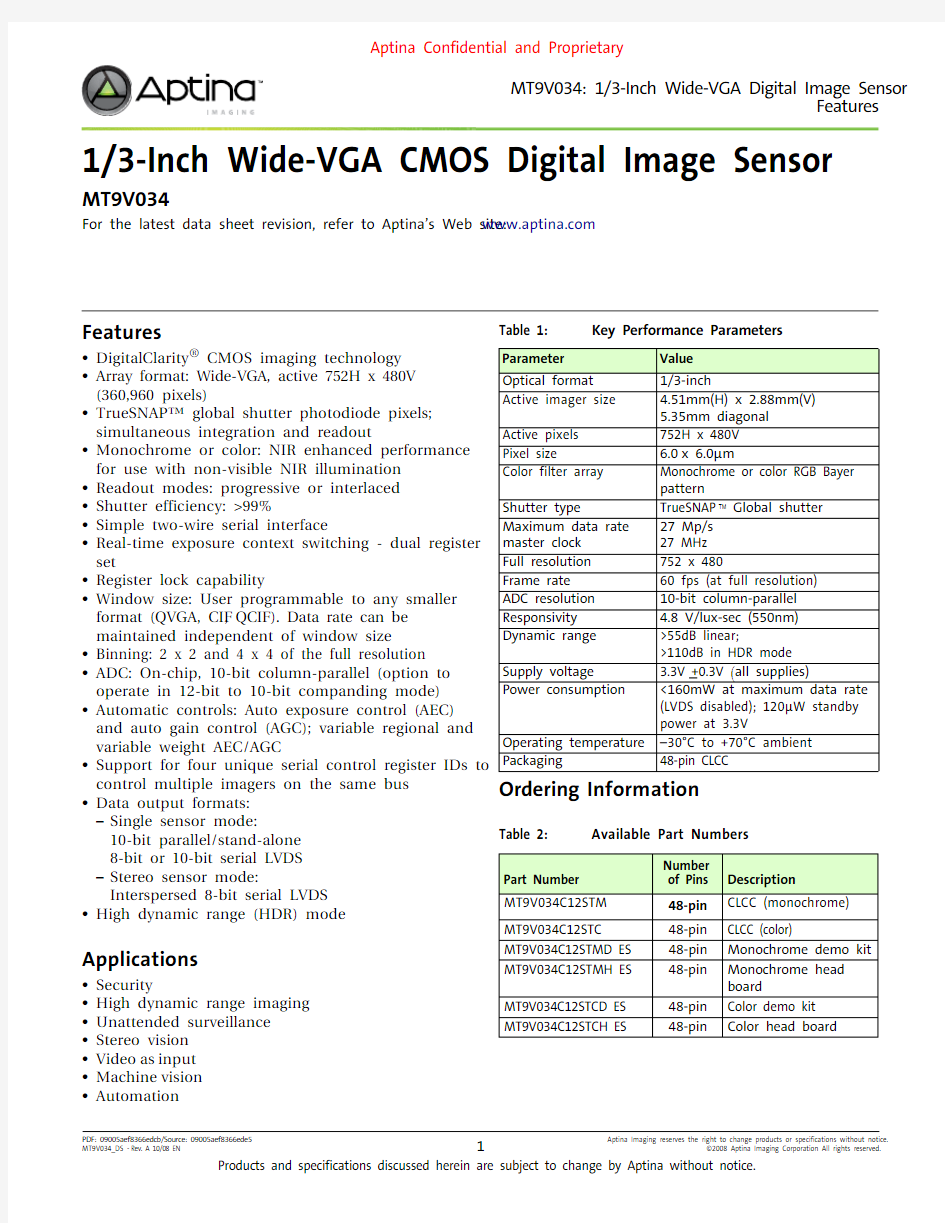
Table 1:
Key Performance Parameters
Ordering Information
Parameter
Value
Optical format 1/3-inch
Active imager size 4.51mm(H) x 2.88mm(V)5.35mm diagonal Active pixels 752H x 480V Pixel size
6.0x 6.0μm
Color filter array Monochrome or color RGB Bayer pattern
Shutter type
TrueSNAP ? Global shutter Maximum data rate master clock 27 Mp/s 27 MHz Full resolution 752 x 480
Frame rate 60 fps (at full resolution)ADC resolution 10-bit column-parallel Responsivity 4.8 V/lux-sec (550nm)Dynamic range >55dB linear;
>110dB in HDR mode Supply voltage
3.3V +0.3V (all supplies)
Power consumption
<160mW at maximum data rate (LVDS disabled); 120μW standby power at 3.3V
Operating temperature –30°C to +70°C ambient Packaging
48-pin CLCC
Table 2:
Available Part Numbers
Part Number Number
of Pins Description MT9V034C12STM 48-pin CLCC (monochrome)MT9V034C12STC
48-pin CLCC (color)
MT9V034C12STMD ES 48-pin Monochrome demo kit MT9V034C12STMH ES 48-pin Monochrome head board
MT9V034C12STCD ES 48-pin Color demo kit MT9V034C12STCH ES
48-pin
Color head board
Table of Contents
Features. . . . . . . . . . . . . . . . . . . . . . . . . . . . . . . . . . . . . . . . . . . . . . . . . . . . . . . . . . . . . . . . . . . . . . . . . . . . . . . . . . . . . . . . . . . . . .1 Applications . . . . . . . . . . . . . . . . . . . . . . . . . . . . . . . . . . . . . . . . . . . . . . . . . . . . . . . . . . . . . . . . . . . . . . . . . . . . . . . . . . . . . . . . . .1 Ordering Information. . . . . . . . . . . . . . . . . . . . . . . . . . . . . . . . . . . . . . . . . . . . . . . . . . . . . . . . . . . . . . . . . . . . . . . . . . . . . . . . . .1 General Description . . . . . . . . . . . . . . . . . . . . . . . . . . . . . . . . . . . . . . . . . . . . . . . . . . . . . . . . . . . . . . . . . . . . . . . . . . . . . . . . . . .6 Pin Descriptions . . . . . . . . . . . . . . . . . . . . . . . . . . . . . . . . . . . . . . . . . . . . . . . . . . . . . . . . . . . . . . . . . . . . . . . . . . . . . . . . . . . . . .8 Pixel Data Format . . . . . . . . . . . . . . . . . . . . . . . . . . . . . . . . . . . . . . . . . . . . . . . . . . . . . . . . . . . . . . . . . . . . . . . . . . . . . . . . . . . .10 Pixel Array Structure . . . . . . . . . . . . . . . . . . . . . . . . . . . . . . . . . . . . . . . . . . . . . . . . . . . . . . . . . . . . . . . . . . . . . . . . . . . . . . .10 Color Device Limitations. . . . . . . . . . . . . . . . . . . . . . . . . . . . . . . . . . . . . . . . . . . . . . . . . . . . . . . . . . . . . . . . . . . . . . . . . . . . . .11 Pixel Binning . . . . . . . . . . . . . . . . . . . . . . . . . . . . . . . . . . . . . . . . . . . . . . . . . . . . . . . . . . . . . . . . . . . . . . . . . . . . . . . . . . . . . .11 Interlaced Readout. . . . . . . . . . . . . . . . . . . . . . . . . . . . . . . . . . . . . . . . . . . . . . . . . . . . . . . . . . . . . . . . . . . . . . . . . . . . . . . . .11 Automatic Black Level Calibration. . . . . . . . . . . . . . . . . . . . . . . . . . . . . . . . . . . . . . . . . . . . . . . . . . . . . . . . . . . . . . . . . . .11 Other Limiting Factors . . . . . . . . . . . . . . . . . . . . . . . . . . . . . . . . . . . . . . . . . . . . . . . . . . . . . . . . . . . . . . . . . . . . . . . . . . . . .11 Output Data Format. . . . . . . . . . . . . . . . . . . . . . . . . . . . . . . . . . . . . . . . . . . . . . . . . . . . . . . . . . . . . . . . . . . . . . . . . . . . . . . . . .12 Output Data Timing. . . . . . . . . . . . . . . . . . . . . . . . . . . . . . . . . . . . . . . . . . . . . . . . . . . . . . . . . . . . . . . . . . . . . . . . . . . . . . . .13 Serial Bus Description . . . . . . . . . . . . . . . . . . . . . . . . . . . . . . . . . . . . . . . . . . . . . . . . . . . . . . . . . . . . . . . . . . . . . . . . . . . . . . . .15 Protocol . . . . . . . . . . . . . . . . . . . . . . . . . . . . . . . . . . . . . . . . . . . . . . . . . . . . . . . . . . . . . . . . . . . . . . . . . . . . . . . . . . . . . . . . . .15 Start Bit. . . . . . . . . . . . . . . . . . . . . . . . . . . . . . . . . . . . . . . . . . . . . . . . . . . . . . . . . . . . . . . . . . . . . . . . . . . . . . . . . . . . . . . . . . .15 Slave Address. . . . . . . . . . . . . . . . . . . . . . . . . . . . . . . . . . . . . . . . . . . . . . . . . . . . . . . . . . . . . . . . . . . . . . . . . . . . . . . . . . . . . .15 Acknowledge Bit. . . . . . . . . . . . . . . . . . . . . . . . . . . . . . . . . . . . . . . . . . . . . . . . . . . . . . . . . . . . . . . . . . . . . . . . . . . . . . . . . . .15 No-Acknowledge Bit . . . . . . . . . . . . . . . . . . . . . . . . . . . . . . . . . . . . . . . . . . . . . . . . . . . . . . . . . . . . . . . . . . . . . . . . . . . . . . .15 Stop Bit. . . . . . . . . . . . . . . . . . . . . . . . . . . . . . . . . . . . . . . . . . . . . . . . . . . . . . . . . . . . . . . . . . . . . . . . . . . . . . . . . . . . . . . . . . .15 Sequence . . . . . . . . . . . . . . . . . . . . . . . . . . . . . . . . . . . . . . . . . . . . . . . . . . . . . . . . . . . . . . . . . . . . . . . . . . . . . . . . . . . . . . . . .16 Bus Idle State. . . . . . . . . . . . . . . . . . . . . . . . . . . . . . . . . . . . . . . . . . . . . . . . . . . . . . . . . . . . . . . . . . . . . . . . . . . . . . . . . . . . . .16 Data Bit Transfer. . . . . . . . . . . . . . . . . . . . . . . . . . . . . . . . . . . . . . . . . . . . . . . . . . . . . . . . . . . . . . . . . . . . . . . . . . . . . . . . . . .16 Two-Wire Serial Interface Sample Read and Write Sequences. . . . . . . . . . . . . . . . . . . . . . . . . . . . . . . . . . . . . . . . . . . . .17 16-Bit Write Sequence. . . . . . . . . . . . . . . . . . . . . . . . . . . . . . . . . . . . . . . . . . . . . . . . . . . . . . . . . . . . . . . . . . . . . . . . . . . . . .17 16-Bit Read Sequence . . . . . . . . . . . . . . . . . . . . . . . . . . . . . . . . . . . . . . . . . . . . . . . . . . . . . . . . . . . . . . . . . . . . . . . . . . . . . .17 8-Bit Write Sequence. . . . . . . . . . . . . . . . . . . . . . . . . . . . . . . . . . . . . . . . . . . . . . . . . . . . . . . . . . . . . . . . . . . . . . . . . . . . . . .18 8-Bit Read Sequence . . . . . . . . . . . . . . . . . . . . . . . . . . . . . . . . . . . . . . . . . . . . . . . . . . . . . . . . . . . . . . . . . . . . . . . . . . . . . . .18 Register Lock. . . . . . . . . . . . . . . . . . . . . . . . . . . . . . . . . . . . . . . . . . . . . . . . . . . . . . . . . . . . . . . . . . . . . . . . . . . . . . . . . . . . . .19 Lock All Registers. . . . . . . . . . . . . . . . . . . . . . . . . . . . . . . . . . . . . . . . . . . . . . . . . . . . . . . . . . . . . . . . . . . . . . . . . . . . . . . .19 Lock Only Read Mode Registers (R0x0D and R0x0E). . . . . . . . . . . . . . . . . . . . . . . . . . . . . . . . . . . . . . . . . . . . . . . . .19 Real-Time Context Switching . . . . . . . . . . . . . . . . . . . . . . . . . . . . . . . . . . . . . . . . . . . . . . . . . . . . . . . . . . . . . . . . . . . . . . .20 Registers . . . . . . . . . . . . . . . . . . . . . . . . . . . . . . . . . . . . . . . . . . . . . . . . . . . . . . . . . . . . . . . . . . . . . . . . . . . . . . . . . . . . . . . . . . . .21 Shadowed Register. . . . . . . . . . . . . . . . . . . . . . . . . . . . . . . . . . . . . . . . . . . . . . . . . . . . . . . . . . . . . . . . . . . . . . . . . . . . . . . . .25 Feature Description . . . . . . . . . . . . . . . . . . . . . . . . . . . . . . . . . . . . . . . . . . . . . . . . . . . . . . . . . . . . . . . . . . . . . . . . . . . . . . . . . .47 Operational Modes . . . . . . . . . . . . . . . . . . . . . . . . . . . . . . . . . . . . . . . . . . . . . . . . . . . . . . . . . . . . . . . . . . . . . . . . . . . . . . . .47 Master Mode. . . . . . . . . . . . . . . . . . . . . . . . . . . . . . . . . . . . . . . . . . . . . . . . . . . . . . . . . . . . . . . . . . . . . . . . . . . . . . . . . . . .47 Simultaneous Master Mode . . . . . . . . . . . . . . . . . . . . . . . . . . . . . . . . . . . . . . . . . . . . . . . . . . . . . . . . . . . . . . . . . . . . . .47 Sequential Master Mode . . . . . . . . . . . . . . . . . . . . . . . . . . . . . . . . . . . . . . . . . . . . . . . . . . . . . . . . . . . . . . . . . . . . . . . . .48 Snapshot Mode . . . . . . . . . . . . . . . . . . . . . . . . . . . . . . . . . . . . . . . . . . . . . . . . . . . . . . . . . . . . . . . . . . . . . . . . . . . . . . . . .48 Slave Mode . . . . . . . . . . . . . . . . . . . . . . . . . . . . . . . . . . . . . . . . . . . . . . . . . . . . . . . . . . . . . . . . . . . . . . . . . . . . . . . . . . . . .49 Signal Path. . . . . . . . . . . . . . . . . . . . . . . . . . . . . . . . . . . . . . . . . . . . . . . . . . . . . . . . . . . . . . . . . . . . . . . . . . . . . . . . . . . . . . . .50 On-Chip Biases. . . . . . . . . . . . . . . . . . . . . . . . . . . . . . . . . . . . . . . . . . . . . . . . . . . . . . . . . . . . . . . . . . . . . . . . . . . . . . . . . . . .50 ADC Voltage Reference . . . . . . . . . . . . . . . . . . . . . . . . . . . . . . . . . . . . . . . . . . . . . . . . . . . . . . . . . . . . . . . . . . . . . . . . . .50 V_Step Voltage Reference . . . . . . . . . . . . . . . . . . . . . . . . . . . . . . . . . . . . . . . . . . . . . . . . . . . . . . . . . . . . . . . . . . . . . . . .51 Chip Version. . . . . . . . . . . . . . . . . . . . . . . . . . . . . . . . . . . . . . . . . . . . . . . . . . . . . . . . . . . . . . . . . . . . . . . . . . . . . . . . . . . .51 Window Control . . . . . . . . . . . . . . . . . . . . . . . . . . . . . . . . . . . . . . . . . . . . . . . . . . . . . . . . . . . . . . . . . . . . . . . . . . . . . . . . . . .51 Blanking Control. . . . . . . . . . . . . . . . . . . . . . . . . . . . . . . . . . . . . . . . . . . . . . . . . . . . . . . . . . . . . . . . . . . . . . . . . . . . . . . . . . .51 Pixel Integration Control . . . . . . . . . . . . . . . . . . . . . . . . . . . . . . . . . . . . . . . . . . . . . . . . . . . . . . . . . . . . . . . . . . . . . . . . . . .52 Total Integration . . . . . . . . . . . . . . . . . . . . . . . . . . . . . . . . . . . . . . . . . . . . . . . . . . . . . . . . . . . . . . . . . . . . . . . . . . . . . . . .52
Changes to Integration Time . . . . . . . . . . . . . . . . . . . . . . . . . . . . . . . . . . . . . . . . . . . . . . . . . . . . . . . . . . . . . . . . . . . . .53 Exposure Indicator . . . . . . . . . . . . . . . . . . . . . . . . . . . . . . . . . . . . . . . . . . . . . . . . . . . . . . . . . . . . . . . . . . . . . . . . . . . . . .54 High Dynamic Range . . . . . . . . . . . . . . . . . . . . . . . . . . . . . . . . . . . . . . . . . . . . . . . . . . . . . . . . . . . . . . . . . . . . . . . . . . . .54 ADC Companding Mode. . . . . . . . . . . . . . . . . . . . . . . . . . . . . . . . . . . . . . . . . . . . . . . . . . . . . . . . . . . . . . . . . . . . . . . . . . . .56 Gain Settings . . . . . . . . . . . . . . . . . . . . . . . . . . . . . . . . . . . . . . . . . . . . . . . . . . . . . . . . . . . . . . . . . . . . . . . . . . . . . . . . . . . . . .57 Changes to Gain Settings. . . . . . . . . . . . . . . . . . . . . . . . . . . . . . . . . . . . . . . . . . . . . . . . . . . . . . . . . . . . . . . . . . . . . . . . .57 Analog Gain . . . . . . . . . . . . . . . . . . . . . . . . . . . . . . . . . . . . . . . . . . . . . . . . . . . . . . . . . . . . . . . . . . . . . . . . . . . . . . . . . . . .58 Digital Gain. . . . . . . . . . . . . . . . . . . . . . . . . . . . . . . . . . . . . . . . . . . . . . . . . . . . . . . . . . . . . . . . . . . . . . . . . . . . . . . . . . . . .58 Black Level Calibration . . . . . . . . . . . . . . . . . . . . . . . . . . . . . . . . . . . . . . . . . . . . . . . . . . . . . . . . . . . . . . . . . . . . . . . . . . . . .59 Row-wise Noise Correction . . . . . . . . . . . . . . . . . . . . . . . . . . . . . . . . . . . . . . . . . . . . . . . . . . . . . . . . . . . . . . . . . . . . . . . . .61 Automatic Gain Control and Automatic Exposure Control . . . . . . . . . . . . . . . . . . . . . . . . . . . . . . . . . . . . . . . . . . . . .61 Pixel Clock Speed . . . . . . . . . . . . . . . . . . . . . . . . . . . . . . . . . . . . . . . . . . . . . . . . . . . . . . . . . . . . . . . . . . . . . . . . . . . . . . . . . .62 Hard Reset of Logic . . . . . . . . . . . . . . . . . . . . . . . . . . . . . . . . . . . . . . . . . . . . . . . . . . . . . . . . . . . . . . . . . . . . . . . . . . . . . . . .63 Soft Reset of Logic . . . . . . . . . . . . . . . . . . . . . . . . . . . . . . . . . . . . . . . . . . . . . . . . . . . . . . . . . . . . . . . . . . . . . . . . . . . . . . . . .63 STANDBY Control . . . . . . . . . . . . . . . . . . . . . . . . . . . . . . . . . . . . . . . . . . . . . . . . . . . . . . . . . . . . . . . . . . . . . . . . . . . . . . . . .63 Monitor Mode Control . . . . . . . . . . . . . . . . . . . . . . . . . . . . . . . . . . . . . . . . . . . . . . . . . . . . . . . . . . . . . . . . . . . . . . . . . . . . .63 Read Mode Options. . . . . . . . . . . . . . . . . . . . . . . . . . . . . . . . . . . . . . . . . . . . . . . . . . . . . . . . . . . . . . . . . . . . . . . . . . . . . . . .63 Column Flip . . . . . . . . . . . . . . . . . . . . . . . . . . . . . . . . . . . . . . . . . . . . . . . . . . . . . . . . . . . . . . . . . . . . . . . . . . . . . . . . . . . .63 Row Flip. . . . . . . . . . . . . . . . . . . . . . . . . . . . . . . . . . . . . . . . . . . . . . . . . . . . . . . . . . . . . . . . . . . . . . . . . . . . . . . . . . . . . . . .64 Pixel Binning. . . . . . . . . . . . . . . . . . . . . . . . . . . . . . . . . . . . . . . . . . . . . . . . . . . . . . . . . . . . . . . . . . . . . . . . . . . . . . . . . . . .64 Row Binning. . . . . . . . . . . . . . . . . . . . . . . . . . . . . . . . . . . . . . . . . . . . . . . . . . . . . . . . . . . . . . . . . . . . . . . . . . . . . . . . . . . .65 Column Binning . . . . . . . . . . . . . . . . . . . . . . . . . . . . . . . . . . . . . . . . . . . . . . . . . . . . . . . . . . . . . . . . . . . . . . . . . . . . . . . .65 Interlaced Readout . . . . . . . . . . . . . . . . . . . . . . . . . . . . . . . . . . . . . . . . . . . . . . . . . . . . . . . . . . . . . . . . . . . . . . . . . . . . . .66 LINE_VALID . . . . . . . . . . . . . . . . . . . . . . . . . . . . . . . . . . . . . . . . . . . . . . . . . . . . . . . . . . . . . . . . . . . . . . . . . . . . . . . . . . . . . .68 LVDS Serial (Stand-Alone/Stereo) Output . . . . . . . . . . . . . . . . . . . . . . . . . . . . . . . . . . . . . . . . . . . . . . . . . . . . . . . . . . . .68 LVDS Output Format. . . . . . . . . . . . . . . . . . . . . . . . . . . . . . . . . . . . . . . . . . . . . . . . . . . . . . . . . . . . . . . . . . . . . . . . . . . . . . .69 LVDS Enable and Disable. . . . . . . . . . . . . . . . . . . . . . . . . . . . . . . . . . . . . . . . . . . . . . . . . . . . . . . . . . . . . . . . . . . . . . . . . . .71 LVDS Data Bus Timing . . . . . . . . . . . . . . . . . . . . . . . . . . . . . . . . . . . . . . . . . . . . . . . . . . . . . . . . . . . . . . . . . . . . . . . . . . . . .72 Electrical Specifications. . . . . . . . . . . . . . . . . . . . . . . . . . . . . . . . . . . . . . . . . . . . . . . . . . . . . . . . . . . . . . . . . . . . . . . . . . . . . . .73 Propagation Delays for PIXCLK and Data Out Signals. . . . . . . . . . . . . . . . . . . . . . . . . . . . . . . . . . . . . . . . . . . . . . . . . .75 Propagation Delays for FRAME_VALID and LINE_VALID Signals . . . . . . . . . . . . . . . . . . . . . . . . . . . . . . . . . . . . . . .75 Two-Wire Serial Bus Timing . . . . . . . . . . . . . . . . . . . . . . . . . . . . . . . . . . . . . . . . . . . . . . . . . . . . . . . . . . . . . . . . . . . . . . . .76 Minimum Master Clock Cycles . . . . . . . . . . . . . . . . . . . . . . . . . . . . . . . . . . . . . . . . . . . . . . . . . . . . . . . . . . . . . . . . . . .77 Package Dimensions . . . . . . . . . . . . . . . . . . . . . . . . . . . . . . . . . . . . . . . . . . . . . . . . . . . . . . . . . . . . . . . . . . . . . . . . . . . . . . . . .80 Appendix A–Power-On Reset and Standby Timing . . . . . . . . . . . . . . . . . . . . . . . . . . . . . . . . . . . . . . . . . . . . . . . . . . . . . .81 Revision History. . . . . . . . . . . . . . . . . . . . . . . . . . . . . . . . . . . . . . . . . . . . . . . . . . . . . . . . . . . . . . . . . . . . . . . . . . . . . . . . . . . . . .82
List of Figures
Figure 1:Block Diagram. . . . . . . . . . . . . . . . . . . . . . . . . . . . . . . . . . . . . . . . . . . . . . . . . . . . . . . . . . . . . . . . . . . . . . . . . . . .6 Figure 2:48-Pin CLCC Package Pinout Diagram . . . . . . . . . . . . . . . . . . . . . . . . . . . . . . . . . . . . . . . . . . . . . . . . . . . . . .7 Figure 3:Typical Configuration (Connection)—Parallel Output Mode. . . . . . . . . . . . . . . . . . . . . . . . . . . . . . . . . . .9 Figure 4:Pixel Array Description . . . . . . . . . . . . . . . . . . . . . . . . . . . . . . . . . . . . . . . . . . . . . . . . . . . . . . . . . . . . . . . . . . .10 Figure 5:Pixel Color Pattern Detail (Top Right Corner) . . . . . . . . . . . . . . . . . . . . . . . . . . . . . . . . . . . . . . . . . . . . . . .11 Figure 6:Spatial Illustration of Image Readout. . . . . . . . . . . . . . . . . . . . . . . . . . . . . . . . . . . . . . . . . . . . . . . . . . . . . . .12 Figure 7:Timing Example of Pixel Data . . . . . . . . . . . . . . . . . . . . . . . . . . . . . . . . . . . . . . . . . . . . . . . . . . . . . . . . . . . . .13 Figure 8:Row Timing and FRAME_VALID/LINE_VALID Signals . . . . . . . . . . . . . . . . . . . . . . . . . . . . . . . . . . . . . . .13 Figure 9:Timing Diagram Showing a Write to R0x09 with the Value 0x0284. . . . . . . . . . . . . . . . . . . . . . . . . . . . .17 Figure 10:Timing Diagram Showing a Read from R0x09; Returned Value 0x0284 . . . . . . . . . . . . . . . . . . . . . . . . .17 Figure 11:Timing Diagram Showing a Bytewise Write to R0x09 with the Value 0x0284 . . . . . . . . . . . . . . . . . . . .18 Figure 12:Timing Diagram Showing a Bytewise Read from R0x09; Returned Value 0x0284 . . . . . . . . . . . . . . . .18 Figure 13:Simultaneous Master Mode Synchronization Waveforms #1. . . . . . . . . . . . . . . . . . . . . . . . . . . . . . . . . .47 Figure 14:Simultaneous Master Mode Synchronization Waveforms #2. . . . . . . . . . . . . . . . . . . . . . . . . . . . . . . . . .48 Figure 15:Sequential Master Mode Synchronization Waveforms . . . . . . . . . . . . . . . . . . . . . . . . . . . . . . . . . . . . . . .48 Figure 16:Snapshot Mode Interface Signals . . . . . . . . . . . . . . . . . . . . . . . . . . . . . . . . . . . . . . . . . . . . . . . . . . . . . . . . . .49 Figure 17:Snapshot Mode Frame Synchronization Waveforms. . . . . . . . . . . . . . . . . . . . . . . . . . . . . . . . . . . . . . . . .49 Figure 18:Slave Mode Operation. . . . . . . . . . . . . . . . . . . . . . . . . . . . . . . . . . . . . . . . . . . . . . . . . . . . . . . . . . . . . . . . . . . .50 Figure 19:Signal Path . . . . . . . . . . . . . . . . . . . . . . . . . . . . . . . . . . . . . . . . . . . . . . . . . . . . . . . . . . . . . . . . . . . . . . . . . . . . . .50 Figure 20:Latency When Changing Integration . . . . . . . . . . . . . . . . . . . . . . . . . . . . . . . . . . . . . . . . . . . . . . . . . . . . . . .53 Figure 21:Sequence of Control Voltages at the HDR Gate. . . . . . . . . . . . . . . . . . . . . . . . . . . . . . . . . . . . . . . . . . . . . .54 Figure 22:Sequence of Voltages in a Piecewise Linear Pixel Response . . . . . . . . . . . . . . . . . . . . . . . . . . . . . . . . . . .55 Figure 23:12- to 10-Bit Companding Chart. . . . . . . . . . . . . . . . . . . . . . . . . . . . . . . . . . . . . . . . . . . . . . . . . . . . . . . . . . .56 Figure 24:Latency of Analog Gain Change When AGC Is Disabled . . . . . . . . . . . . . . . . . . . . . . . . . . . . . . . . . . . . . .57 Figure 25:Tiled Sample . . . . . . . . . . . . . . . . . . . . . . . . . . . . . . . . . . . . . . . . . . . . . . . . . . . . . . . . . . . . . . . . . . . . . . . . . . . .59 Figure 26:Black Level Calibration Flow Chart. . . . . . . . . . . . . . . . . . . . . . . . . . . . . . . . . . . . . . . . . . . . . . . . . . . . . . . . .59 Figure 27:Controllable and Observable AEC/AGC Registers. . . . . . . . . . . . . . . . . . . . . . . . . . . . . . . . . . . . . . . . . . . .62 Figure 28:Readout of Six Pixels in Normal and Column Flip Output Mode. . . . . . . . . . . . . . . . . . . . . . . . . . . . . . .64 Figure 29:Readout of Six Rows in Normal and Row Flip Output Mode . . . . . . . . . . . . . . . . . . . . . . . . . . . . . . . . . .64 Figure 30:Readout of 8 Pixels in Normal and Row Bin Output Mode . . . . . . . . . . . . . . . . . . . . . . . . . . . . . . . . . . . .65 Figure 31:Readout of 8 Pixels in Normal and Column Bin Output Mode. . . . . . . . . . . . . . . . . . . . . . . . . . . . . . . . .66 Figure 32:Spatial Illustration of Interlaced Image Readout. . . . . . . . . . . . . . . . . . . . . . . . . . . . . . . . . . . . . . . . . . . . .67 Figure 33:Different LINE_VALID Formats. . . . . . . . . . . . . . . . . . . . . . . . . . . . . . . . . . . . . . . . . . . . . . . . . . . . . . . . . . . .68 Figure 34:Serial Output Format for a 6x2 Frame . . . . . . . . . . . . . . . . . . . . . . . . . . . . . . . . . . . . . . . . . . . . . . . . . . . . . .69 Figure 35:LVDS Timing . . . . . . . . . . . . . . . . . . . . . . . . . . . . . . . . . . . . . . . . . . . . . . . . . . . . . . . . . . . . . . . . . . . . . . . . . . . .72 Figure 36:Propagation Delays for PIXCLK and Data Out Signals. . . . . . . . . . . . . . . . . . . . . . . . . . . . . . . . . . . . . . . .75 Figure 37:Propagation Delays for FRAME_VALID and LINE_VALID Signals. . . . . . . . . . . . . . . . . . . . . . . . . . . . . .75 Figure 38:Two-wire Serial Bus Timing . . . . . . . . . . . . . . . . . . . . . . . . . . . . . . . . . . . . . . . . . . . . . . . . . . . . . . . . . . . . . . .76 Figure 39:Serial Host Interface Start Condition Timing. . . . . . . . . . . . . . . . . . . . . . . . . . . . . . . . . . . . . . . . . . . . . . . .77 Figure 40:Serial Host Interface Stop Condition Timing . . . . . . . . . . . . . . . . . . . . . . . . . . . . . . . . . . . . . . . . . . . . . . . .77 Figure 41:Serial Host Interface Data Timing for Write . . . . . . . . . . . . . . . . . . . . . . . . . . . . . . . . . . . . . . . . . . . . . . . . .77 Figure 42:Serial Host Interface Data Timing for Read . . . . . . . . . . . . . . . . . . . . . . . . . . . . . . . . . . . . . . . . . . . . . . . . .78 Figure 43:Acknowledge Signal Timing After an 8-Bit WRITE to the Sensor. . . . . . . . . . . . . . . . . . . . . . . . . . . . . . .78 Figure 44:Acknowledge Signal Timing After an 8-Bit READ from the Sensor . . . . . . . . . . . . . . . . . . . . . . . . . . . . .78 Figure 45:Typical Quantum Efficiency – Color. . . . . . . . . . . . . . . . . . . . . . . . . . . . . . . . . . . . . . . . . . . . . . . . . . . . . . . .79 Figure 46:Typical Quantum Efficiency – Monochrome . . . . . . . . . . . . . . . . . . . . . . . . . . . . . . . . . . . . . . . . . . . . . . . .79 Figure 47:48-Pin CLCC Package Outline Drawing. . . . . . . . . . . . . . . . . . . . . . . . . . . . . . . . . . . . . . . . . . . . . . . . . . . . .80 Figure 48:Power-up, Reset, Clock and Standby Sequence. . . . . . . . . . . . . . . . . . . . . . . . . . . . . . . . . . . . . . . . . . . . . .81
List of Tables
Table 1:Key Performance Parameters. . . . . . . . . . . . . . . . . . . . . . . . . . . . . . . . . . . . . . . . . . . . . . . . . . . . . . . . . . . . . . .1 Table 2:Available Part Numbers. . . . . . . . . . . . . . . . . . . . . . . . . . . . . . . . . . . . . . . . . . . . . . . . . . . . . . . . . . . . . . . . . . . .1 Table 3:Pin Descriptions . . . . . . . . . . . . . . . . . . . . . . . . . . . . . . . . . . . . . . . . . . . . . . . . . . . . . . . . . . . . . . . . . . . . . . . . . .8 Table 4:Frame Time . . . . . . . . . . . . . . . . . . . . . . . . . . . . . . . . . . . . . . . . . . . . . . . . . . . . . . . . . . . . . . . . . . . . . . . . . . . . .13 Table 5:Frame Time—Long Integration Time . . . . . . . . . . . . . . . . . . . . . . . . . . . . . . . . . . . . . . . . . . . . . . . . . . . . . .14 Table 6:Slave Address Modes . . . . . . . . . . . . . . . . . . . . . . . . . . . . . . . . . . . . . . . . . . . . . . . . . . . . . . . . . . . . . . . . . . . . .16 Table 7:Real-Time Context-Switchable Registers . . . . . . . . . . . . . . . . . . . . . . . . . . . . . . . . . . . . . . . . . . . . . . . . . . .20 Table 8:Default Register Descriptions . . . . . . . . . . . . . . . . . . . . . . . . . . . . . . . . . . . . . . . . . . . . . . . . . . . . . . . . . . . . .21 Table 9:Register Descriptions. . . . . . . . . . . . . . . . . . . . . . . . . . . . . . . . . . . . . . . . . . . . . . . . . . . . . . . . . . . . . . . . . . . . .25 Table 10:LVDS Packet Format in Stand-Alone Mode . . . . . . . . . . . . . . . . . . . . . . . . . . . . . . . . . . . . . . . . . . . . . . . . .69 Table 11:LVDS Packet Format in Stereoscopy Mode (Stereoscopy Mode Bit Asserted) . . . . . . . . . . . . . . . . . . .70 Table 12:Reserved Words in the Pixel Data Stream . . . . . . . . . . . . . . . . . . . . . . . . . . . . . . . . . . . . . . . . . . . . . . . . . . .70 Table 13:SER_DATAOUT_* state . . . . . . . . . . . . . . . . . . . . . . . . . . . . . . . . . . . . . . . . . . . . . . . . . . . . . . . . . . . . . . . . . . .71 Table 14:SHFT_CLK_* state. . . . . . . . . . . . . . . . . . . . . . . . . . . . . . . . . . . . . . . . . . . . . . . . . . . . . . . . . . . . . . . . . . . . . . . .71 Table 15:LVDS AC Timing Specifications. . . . . . . . . . . . . . . . . . . . . . . . . . . . . . . . . . . . . . . . . . . . . . . . . . . . . . . . . . . .72 Table 16:DC Electrical Characteristics Over Temperature. . . . . . . . . . . . . . . . . . . . . . . . . . . . . . . . . . . . . . . . . . . . .73 Table 17:DC Electrical Characteristics . . . . . . . . . . . . . . . . . . . . . . . . . . . . . . . . . . . . . . . . . . . . . . . . . . . . . . . . . . . . . .73 Table 18:Absolute Maximum Ratings. . . . . . . . . . . . . . . . . . . . . . . . . . . . . . . . . . . . . . . . . . . . . . . . . . . . . . . . . . . . . . .74 Table 19:AC Electrical Characteristics . . . . . . . . . . . . . . . . . . . . . . . . . . . . . . . . . . . . . . . . . . . . . . . . . . . . . . . . . . . . . .74 Table 20:Two-Wire Serial Bus Timing Parameters. . . . . . . . . . . . . . . . . . . . . . . . . . . . . . . . . . . . . . . . . . . . . . . . . . . .76
General Description
The MT9V034 is a 1/3-inch wide-VGA format CMOS active-pixel digital image sensor
with TrueSNAP? global shutter and high dynamic range (HDR) operation. The sensor
has specifically been designed to support the demanding interior and exterior surveil-
lance imaging needs, which makes this part ideal for a wide variety of imaging applica-
tions in real-world environments.
This wide-VGA CMOS image sensor features DigitalClarity?Aptina’s breakthrough
low-noise CMOS imaging technology that achieves CCD image quality (based on
signal-to-noise ratio and low-light sensitivity) while maintaining the inherent size, cost,
and integration advantages of CMOS.
The active imaging pixel array is 752H x480V. It incorporates sophisticated camera func-
tions on-chip—such as binning 2x2 and 4x4, to improve sensitivity when operating in
smaller resolutions—as well as windowing, column and row mirroring. It is program-
mable through a simple two-wire serial interface.
The MT9V034 can be operated in its default mode or be programmed for frame size,
exposure, gain setting, and other parameters. The default mode outputs a
wide-VGA-size image at 60 frames per second (fps).
An on-chip analog-to-digital converter (ADC) provides 10 bits per pixel. A 12-bit resolu-
tion companded for 10 bits for small signals can be alternatively enabled, allowing more
accurate digitization for darker areas in the image.
In addition to a traditional, parallel logic output the MT9V034 also features a serial low-
voltage differential signaling (LVDS) output. The sensor can be operated in a stereo-
camera, and the sensor, designated as a stereo-master, is able to merge the data from
itself and the stereo-slave sensor into one serial LVDS stream.
The sensor is designed to operate in a wide temperature range (–30°C to +70°C). Figure 1: Block Diagram
Pin Descriptions
Table 3: Pin Descriptions
48-Pin CLCC
Numbers Symbol Type Description Note
D GND.1
to
29RSVD Input Connect
10SER_DATAIN_N Input Serial data in for stereoscopy (differential negative). Tie to 1KΩ
pull-up (to 3.3V) in non-stereoscopy mode.
11SER_DATAIN_P Input Serial data in for stereoscopy (differential positive). Tie to D GND in
non-stereoscopy mode.
8BYPASS_CLKIN_N Input Input bypass shift-CLK (differential negative). Tie to 1KΩ pull-up
(to 3.3V) in non-stereoscopy mode.
9BYPASS_CLKIN_P Input Input bypass shift-CLK (differential positive). Tie to D GND in non-
stereoscopy mode.
23EXPOSURE Input Rising edge starts exposure in snapshot and slave modes.
25SCLK Input Two-wire serial interface clock. Connect to V DD with 1.5K resistor
even when no other two-wire serial interface peripheral is
attached.
28OE Input D OUT enable pad, active HIGH.2 30S_CTRL_ADR0Input Two-wire serial interface slave address select (see Table6 on
page16).
31S_CTRL_ADR1Input Two-wire serial interface slave address select (see Table6 on
page16).
32RESET_BAR Input Asynchronous reset. All registers assume defaults.
33STANDBY Input Shut down sensor operation for power saving.
47SYSCLK Input Master clock (26.6 MHz; 13MHz – 27MHz).
24S DATA I/O Two-wire serial interface data. Connect to V DD with 1.5K resistor
even when no other two-wire serial interface peripheral is
attached.
22STLN_OUT I/O Output in master mode—start line sync to drive slave chip in-
phase; input in slave mode.
26STFRM_OUT I/O Output in master mode—start frame sync to drive a slave chip in-
phase; input in slave mode.
20LINE_VALID Output Asserted when D OUT data is valid.
21FRAME_VALID Output Asserted when D OUT data is valid.
15D OUT5Output Parallel pixel data output 5.
16D OUT6Output Parallel pixel data output 6.
17D OUT7Output Parallel pixel data output 7.
18D OUT8Output Parallel pixel data output 8.
19D OUT9Output Parallel pixel data output 9.
27LED_OUT Output LED strobe output.
41D OUT4Output Parallel pixel data output 4.
42D OUT3Output Parallel pixel data output 3.
43D OUT2Output Parallel pixel data output 2.
44D OUT1Output Parallel pixel data output 1.
45D OUT0Output Parallel pixel data output 0.
46PIXCLK Output Pixel clock out. D OUT is valid on rising edge of this clock.
2SHFT_CLKOUT_N Output Output shift CLK (differential negative).
3SHFT_CLKOUT_P Output Output shift CLK (differential positive).
4SER_DATAOUT_N Output Serial data out (differential negative).
Notes:
1.Pin 29, (RSVD) must be tied to GND.
2.Output enable (OE) tri-states signals D OUT 0–D OUT 9, LINE_VALID, FRAME_VALID, and PIXCLK.
3.No connect. These pins must be left floating for proper operation.
Figure 3: Typical Configuration (Connection)—Parallel Output Mode
Note:LVDS signals are to be left floating.
5SER_DATAOUT_P
Output Serial data out (differential positive).1,14V DD Supply Digital power 3.3V.35,39V AA Supply Analog power 3.3V.40VAAPIX Supply Pixel power 3.3V.
6V DD LVDS Supply Dedicated power for LVDS pads.7,12LVDSGND Ground Dedicated GND for LVDS pads.13,48D GND Ground Digital GND.34,38A GND Ground Analog GND.36,37
NC NC
No connect.
3
Table 3:
Pin Descriptions (continued)
48-Pin CLCC Numbers
Symbol Type Description
Note
Pixel Data Format
Pixel Array Structure
The MT9V034 pixel array is configured as 809 columns by 499 rows, shown in Figure4.
The dark pixels are optically black and are used internally to monitor black level. Of the
left 52 columns, 36 are dark pixels used for row noise correction. Of the top 14 rows of
pixels, two of the dark rows are used for black level correction. Also, three black rows
from the top black rows can be read out by setting the Show Dark Rows bit in the Read
Mode register; setting Show Dark Columns will display the 36 dark columns. There are
753 columns by 481 rows of optically active pixels. While the sensor's format is 752 x 480,
one additional active column and active row are included for use when horizontal or
vertical mirrored readout is enabled, to allow readout to start on the same pixel. This one
pixel adjustment is always performed, for monochrome or color versions. The active
area is surrounded with optically transparent dummy pixels to improve image unifor-
mity within the active area. Neither dummy pixels nor barrier pixels can be read out. Figure 4: Pixel Array Description
Color Device Limitations
The color version of the MT9V034 does not support or offers reduced performance for
the following functionalities.
Pixel Binning
Pixel binning is done on immediate neighbor pixels only, no facility is provided to skip
pixels according to a Bayer pattern. Therefore, the result of binning combines pixels of
different colors. See “Pixel Binning” on page64 for additional information. Interlaced Readout
Interlaced readout yields one field consisting only of red and green pixels and another
consisting only of blue and green pixels. This is due to the Bayer pattern of the CFA. Automatic Black Level Calibration
When the color bit is set (R0x0F[1]=1), the sensor uses black level correction values from
one green plane, which are applied to all colors. To use the calibration value based on all
dark pixels' offset values, the color bit should be cleared.
Other Limiting Factors
Black level correction and row-wise noise correction are applied uniformly to each color.
The row-wise noise correction algorithm does not work well in color sensors. Automatic
exposure and gain control calculations are made based on all three colors, not just the
green channel. High dynamic range does operate in color; however, Aptina strongly
recommends limiting use to linear operation where good color fidelity is required.
Output Data Format
The MT9V034 image data can be read out in a progressive scan or interlaced scan mode.
Valid image data is surrounded by horizontal and vertical blanking, as shown in Figure6.
The amount of horizontal and vertical blanking is programmable through R0x05 and
R0x06, respectively (R0xCD and R0xCE for context B). LV is HIGH during the shaded
region of the figure. See “Output Data Timing” on page13 for the description of FV
timing.
Figure 6: Spatial Illustration of Image Readout
The PIXCLK is a nominally inverted version of the master clock (SYSCLK). This allows PIXCLK to be used as a clock to latch the data. However, when column bin 2 is enabled, the PIXCLK is HIGH for one complete master clock master period and then LOW for one complete master clock period; when column bin 4 is enabled, the PIXCLK is HIGH for two complete master clock periods and then LOW for two complete master clock periods. It is continuously enabled, even during the blanking period. Setting R0x72 bit[4]=1 causes the MT9V034 to invert the polarity of the PIXCLK.The parameters P1, A, Q, and P2 in Figure 8 are defined in Table 4.
Figure 8: Row Timing and FRAME_VALID/LINE_VALID Signals
Table 4: Frame Time
Parameter
Name
Equation Default Timing at 26.66 MHz A
Active data time
Context A: R0x04 Context B: R0xCC 752 pixel clocks = 752 master = 28.20μs P1Frame start blanking
Context A: R0x05 - 23Context B: R0xCD - 2371 pixel clocks = 71master = 2.66μs
P2Frame end blanking
23 (fixed)
23 pixel clocks = 23 master = 0.86μs
Q Horizontal blanking
Context A: R0x05Context B: R0xCD
94 pixel clocks = 94 master = 3.52μs
Sensor timing is shown above in terms of pixel clock and master clock cycles (refer to Figure 7 on page 13). The recommended master clock frequency is 26.66 MHz. The vertical blanking and the total frame time equations assume that the integration time (Coarse Shutter Width plus Fine Shutter Width) is less than the number of active rows plus the blanking rows minus the overhead rows:
Window Height + Vertical Blanking – 2
(EQ 1)
If this is not the case, the number of integration rows must be used instead to determine the frame time, as shown in Table 5. In this example it is assumed that the Coarse Shutter Width Control is programmed with 523 rows, and the Fine Shutter Width Total is zero. For Simultaneous mode, if the exposure time registers (Coarse Shutter Width Total plus Fine Shutter Width Total) exceed the total readout time, then the vertical blanking time is internally extended automatically to adjust for the additional integration time
required. This extended value is not written back to the vertical blanking registers. The Vertical Blank register can be used to adjust frame-to-frame readout time. This register does not affect the exposure time but it may extend the readout time.
Notes:
1.The MT9V034 uses column parallel analog-digital converters, thus short row timing is not possible. The minimum total row time is 690 columns (horizontal width + horizontal blanking). The mini-mum horizontal blanking is 61. When the window width is set below 627, horizontal blanking must be increased.
A+Q
Row time
Context A: R0x04 + R0x05Context B: R0xCC + R0xCD 846 pixel clocks = 846 master = 31.72μs
V Vertical blanking
Context A: (R0x06) x (A + Q) + 4Context B: (R0xCE) x (A + Q) + 438,074 pixel clocks = 38,074 master = 1.43ms
Nrows x (A + Q)Frame valid time
Context A: (R0x03) × (A + Q)Context B: (R0xCB) x (A + Q)406,080 pixel clocks = 406,080 master = 15.23ms
F Total frame time
V + (Nrows x (A + Q))
444,154 pixel clocks = 444,154 master = 16.66ms
Table 5:
Frame Time—Long Integration Time
Parameter
Name
Equation
(Number of Master Clock Cycles)
Default Timing at 26.66 MHz V’
Vertical blanking (long integration time)Context A: (R0x0B + 2 - R0x03) × (A + Q) + R0xD5 + 4Context B: (R0xD2 + 2 - R0xCB) x (A + Q) + R0xD8 + 438,074 pixel clocks = 38,074 master = 1.43ms
F
Total frame time (long integration time)
Context A: (R0x0B + 2) × (A + Q) + R0xD5 + 4Context B: (R0xD2 + 2) x (A + Q) + R0xD8 + 4
444,154 pixel clocks = 444,154 master = 16.66ms
Table 4:
Frame Time (continued)
Parameter Name Equation
Default Timing at 26.66 MHz
Serial Bus Description
Registers are written to and read from the MT9V034 through the two-wire serial inter-
face bus. The MT9V034 is a serial interface slave with four possible IDs (0x90, 0x98, 0xB0
and 0xB8) determined by the S_CTRL_ADR0 and S_CTRL_ADR1 input pins. Data is
transferred into the MT9V034 and out through the serial data (S DATA) line. The S DATA
line is pulled up to V DD off-chip by a 1.5KΩ resistor. Either the slave or master device can
pull the S DATA line down—the serial interface protocol determines which device is
allowed to pull the S DATA line down at any given time. The registers are 16-bit wide, and
can be accessed through 16- or 8-bit two-wire serial interface sequences.
Protocol
The two-wire serial interface defines several different transmission codes, as shown in
the following sequence:
1.a start bit
2.the slave device 8-bit address
3.a(n) (no) acknowledge bit
4.an 8-bit message
5.a stop bit
Start Bit
The start bit is defined as a HIGH-to-LOW transition of the data line while the clock line
is HIGH.
Slave Address
The 8-bit address of a two-wire serial interface device consists of 7 bits of address and
1bit of direction. A “0” in the LSB of the address indicates write mode, and a “1” indi-
cates read mode. As indicated above, the MT9V034 allows four possible slave addresses
determined by the two input pins, S_CTRL_ADR0 and S_CTRL_ADR1. Acknowledge Bit
The master generates the acknowledge clock pulse. The transmitter (which is the master
when writing, or the slave when reading) releases the data line, and the receiver indi-
cates an acknowledge bit by pulling the data line LOW during the acknowledge clock
pulse.
No-Acknowledge Bit
The no-acknowledge bit is generated when the data line is not pulled down by the
receiver during the acknowledge clock pulse. A no-acknowledge bit is used to terminate
a read sequence.
Stop Bit
The stop bit is defined as a LOW-to-HIGH transition of the data line while the clock line
is HIGH.
Sequence
A typical READ or WRITE sequence begins by the master sending a start bit. After the
start bit, the master sends the slave device’s 8-bit address. The last bit of the address
determines if the request is a read or a write, where a “0” indicates a WRITE and a “1”
indicates a READ. The slave device acknowledges its address by sending an acknowledge
bit back to the master.
If the request was a WRITE, the master then transfers the 8-bit register address to which
a WRITE should take place. The slave sends an acknowledge bit to indicate that the
register address has been received. The master then transfers the data 8 bits at a time,
with the slave sending an acknowledge bit after each 8 bits. The MT9V034 uses 16-bit
data for its internal registers, thus requiring two 8-bit transfers to write to one register.
After 16 bits are transferred, the register address is automatically incremented, so that
the next 16 bits are written to the next register address. The master stops writing by
sending a start or stop bit.
A typical READ sequence is executed as follows. First the master sends the write mode
slave address and 8-bit register address, just as in the write request. The master then
sends a start bit and the read mode slave address. The master then clocks out the register
data 8 bits at a time. The master sends an acknowledge bit after each 8-bit transfer. The
register address is automatically incremented after every 16 bits is transferred. The data
transfer is stopped when the master sends a no-acknowledge bit. The MT9V034 allows
for 8-bit data transfers through the two-wire serial interface by writing (or reading) the
most significant 8 bits to the register and then writing (or reading) the least significant 8
bits to Byte-Wise Address register (0x0F0).
Bus Idle State
The bus is idle when both the data and clock lines are HIGH. Control of the bus is initi-
ated with a start bit, and the bus is released with a stop bit. Only the master can generate
the start and stop bits.
Table 6: Slave Address Modes
{S_CTRL_ADR1, S_CTRL_ADR0}Slave Address Write/Read Mode
000x90Write
0x91Read
010x98Write
0x99Read
100xB0Write
0xB1Read
110xB8Write
0xB9Read
Data Bit Transfer
One data bit is transferred during each clock pulse. The two-wire serial interface clock
pulse is provided by the master. The data must be stable during the HIGH period of the
serial clock—it can only change when the two-wire serial interface clock is LOW. Data is
transferred 8 bits at a time, followed by an acknowledge bit.
Two-Wire Serial Interface Sample Read and Write Sequences
16-Bit Write Sequence
A typical write sequence for writing 16 bits to a register is shown in Figure9. A start bit
given by the master, followed by the write address, starts the sequence. The image sensor
then gives an acknowledge bit and expects the register address to come first, followed by
the 16-bit data. After each 8-bit the image sensor gives an acknowledge bit. All 16 bits
must be written before the register is updated. After 16 bits are transferred, the register
address is automatically incremented, so that the next 16 bits are written to the next
register. The master stops writing by sending a start or stop bit.
Figure 9: Timing Diagram Showing a Write to R0x09 with the Value 0x0284
16-Bit Read Sequence
A typical read sequence is shown in Figure10. First the master has to write the register
address, as in a write sequence. Then a start bit and the read address specifies that a read
is about to happen from the register. The master then clocks out the register data 8 bits
at a time. The master sends an acknowledge bit after each 8-bit transfer. The register
address is auto-incremented after every 16 bits is transferred. The data transfer is
stopped when the master sends a no-acknowledge bit.
Figure 10: Timing Diagram Showing a Read from R0x09; Returned Value 0x0284
8-Bit Read Sequence
To read one byte at a time the same special register address is used for the lower byte.
The upper 8 bits are read from the desired register. By following this with a read from the
Bytewise Address register (R0xF0) the lower 8 bits are accessed (Figure12). The master
sets the no-acknowledge bits shown.
Figure 12: Timing Diagram Showing a Bytewise Read from R0x09; Returned Value 0x0284
Register Lock
Included in the MT9V034 is a register lock (R0xFE) feature that can be used as a solution
to reduce the probability of an inadvertent noise-triggered two-wire serial interface
write to the sensor. All registers, or only the Read Mode registers–R0x0D and R0x0E, can
be locked. It is important to prevent an inadvertent two-wire serial interface write to the
Read Mode registers in automotive applications since this register controls the image
orientation and any unintended flip to an image can cause serious results.
At power-up, the register lock defaults to a value of 0xBEEF, which implies that all
registers are unlocked and any two-wire serial interface writes to the register gets
committed.
Lock All Registers
If a unique pattern (0xDEAD) to R0xFE is programmed, any subsequent two-wire serial
interface writes to registers (except R0xFE) are NOT committed. Alternatively, if the user
writes a 0xBEEF to the register lock register, all registers are unlocked and any
subsequent two-wire serial interface writes to the register are committed.
Lock Only Read Mode Registers (R0x0D and R0x0E)
If a unique pattern (0xDEAF) to R0xFE is programmed, any subsequent two-wire serial
interface writes to R0x0D or R0x0E are NOT committed. Alternatively, if the user writes a
0xBEEF to register lock register, registers R0x0D and R0x0E are unlocked and any
subsequent two-wire serial interface writes to these registers are committed.
Real-Time Context Switching
In the MT9V034, the user may switch between two full register sets (listed in Table7) by
writing to a context switch change bit in register 0x07. This context switch will change all
registers (no shadowing) at the frame start time and have the new values apply to the
immediate next exposure and readout time.
.
Table 7: Real-Time Context-Switchable Registers
Register Name Register Number (Hex) For Context A Register Number (Hex) for Context B Column Start0x010xC9
Row Start0x020xCA
Window Height0x030xCB
Window Width0x040xCC
Horizontal Blanking0x050xCD
Vertical Blanking0x060xCE
Coarse Shutter Width 10x080xCF
Coarse Shutter Width 20x090xD0
Coarse Shutter Width Control0x0A0xD1
Coarse Shutter Width Total0x0B0xD2
Fine Shutter Width 10xD30xD6
Fine Shutter Width 20xD40xD7
Fine Shutter Width Total0xD50xD8
Read Mode 0x0D [5:0]0x0E [5:0]
High Dynamic Range enable0x0F [0]0x0F [8]
ADC Resolution Control0x1C [1:0]0x1C [9:8]
V1 Control – V4 Control0x31 – 0x340x39 –0x3C
Analog Gain Control0x350x36
Row Noise Correction Control 10x70 [1:0]0x70 [9:8]
Tiled Digital Gain0x80 [3:0] – 0x98 [3:0]0x80 [11:8] – 0x98 [11:8]
AEC/AGC Enable0xAF [1:0]0xAF [9:8]