SY87725L
2.5Gbps GPON/BPON ONU SERDES
Micrel Inc. ? 2180 Fortune Drive ? San Jose, CA 95131 ? USA ? tel +1 (408) 944-0800 ? fax + 1 (408) 474-1000 ? https://www.doczj.com/doc/4d7511587.html, General Description
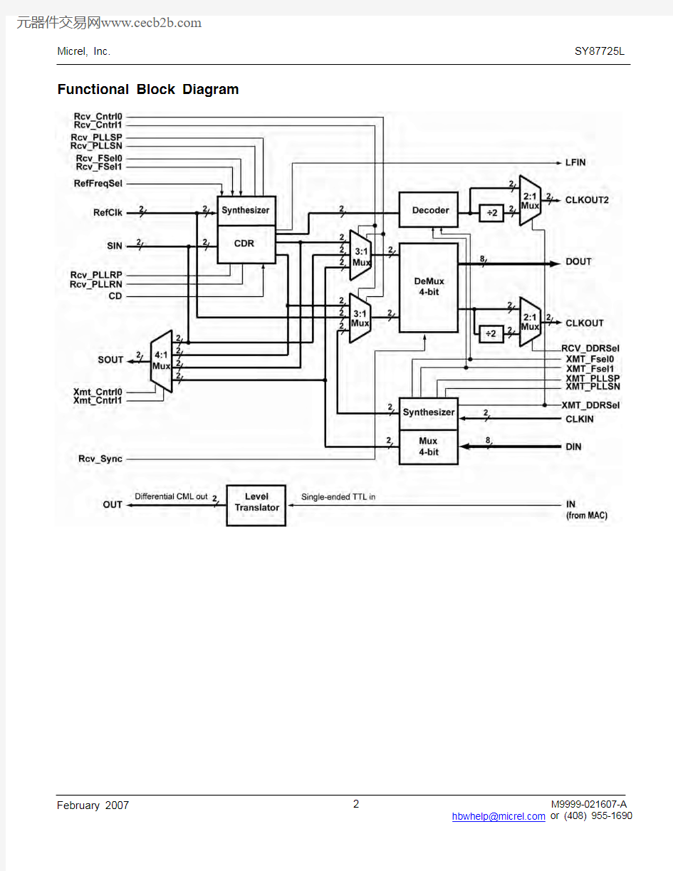
The SY87725L is a single chip transceiver for data rates
up to 2.5Gbps. On the receive side, it includes a
complete clock recovery and data retiming circuit with
an integrated 4-bit serial-to-parallel data converter. On
the transmit side, it includes a synthesizer with an
integrated 4-bit parallel-to-serial data converter.
The SY87725L receiver has a synthesizer that
generates an internal clock from an externally supplied
TTL or PECL REFCLK that can be either 155.52MHz or
77.76MHz. This internal clock can be used by the clock
recovery PLL if an absence of transitions on the input
serial data stream prevents normal clock recovery. This
enables it to provide a stable clock source in the
absence of transitions on the incoming serial data
stream.
The transmit synthesizer uses the CLKIN parallel data
clock to generate its own serial rate clock locked to
CLKIN. This enables the transmit and receive to operate
at different data rates.
The serial interface for both the transmit and receive
functions feature industry standard high-speed
differential CML I/O. The parallel interfaces feature high-
speed LVDS I/O with an internal 100?termination on
the LVDS inputs.
The first bit for the serial-to-parallel conversion can be
moved using the RCV_SYNC input. The RCV_SYNC
input enables the parallel word boundary to move up in
time by one bit time for each pulse. This allows it to in
effect “swallow” one bit each time the RCV_SYNC pulse
is asserted.
Datasheets and support documentation can be found on
Micrel’s web site at: https://www.doczj.com/doc/4d7511587.html,.
Features
?Single 3.3V supply and 1W typ. power consumption
? 2.5G/1.25G/625Mbps down stream
? 1.25G/625M/156Mbps up stream
?4-bit Serdes with LVDS interfaces
?Serial Data input sensitivity of 30mV typical
?Training mode for fast lock acquisition
?Link Fault Indicator (LFIN: “HIGH” = Locked)
?Separate training and MUX synthesizers
?Loop back function for diagnostics
?TTL–CML Translator for MAC-to-Laser diode driver
burst control
?Selectable double data rate option for low cost
FPGA/ASIC MAC implementation
?Available in Pb-Free (10mm x 10mm) 64-pin
EPAD-TQFP
Applications
?BPON/GPON/GEPON/EPON
Markets
?FTTH/FTTP
Functional Block Diagram
64-Pin EPAD-TQFP (T64-1) Ordering Information
Part Number Package
Type
Operating
Range
Package Marking
Lead
Finish
SY87725LHY H64-1Industrial
SY87725LHG with
Pb-Free bar-line indicator
Pb-Free
Matte-Sn
SY87725LHYTR(2)H64-1Industrial
SY87725LHG with
Pb-Free bar-line indicator
Pb-Free
Matte-Sn
Notes:
1.Contact factory for die availability. Dice are guaranteed at T A = 25o C, DC electricals only.
2.Tape and Reel.
RECEIVE SECTION SIGNALS
Pin Number Pin Name Pin Description
55, 56SINP, SINN Serial Data In (Differential LVPECL Input): This input receives the serial differential data stream. An internal PLL recovers the embedded clock and data.
60, 61REFCLKP,
REFCLKN,
Reference Clock (TTL or Differential LVPECL Input): This input accepts either single-
ended TTL or differential LVPECL signals and is used as the reference for the internal
frequency synthesizer and the “training” frequency for the receiver PLL to keep it
centered in the absence of data at the SIN input. The REFCLKN input has an internal
reference circuit that applies the threshold voltage in case of a single-ended TTL-
signal at REFCLKP. REFCLKN has an internal 75k? to GND and can be left open
in that case.
15REFFREQSEL Reference Clock Frequency Select (TTL Input): Selects REFCLK frequency of 77.76MHz when LOW or 155.52MHz when HIGH.
6, 7RCV_PLLRP,
RCV_PLLRN
Clock Recovery PLL Loop Filter: External loop filter pins for the receive PLL.
1, 2RCV_PLLSN,
RCV_PLLSP
Clock Synthesis PLL Loop Filter: External loop filter pins for the clock synthesis PLL.
59RCV_SYNC Receive Synchronizer (TTL Input): Single-ended asynchronous input to set the word boundary on the 4-bit parallel data
3, 5RCV_FSEL0,
RCV_FSEL1
Receive Frequency Control (TTL Inputs): Two single-ended frequency selects for
receive synthesizer.
39, 40, 41, 42, 43, 44, 45, 46DOUTOP, DOUT0N,
DOUT1P, DOUT1N,
DOUT2P, DOUT2N,
DOUT3P, DOUT3N
Parallel Data Out (LVDS Outputs): These are the four pairs of receive parallel data
outputs.
33, 34CLKOUT2P,
CLKOUT2N
Parallel Clock Out (LVDS Output): This output is the recovered clock at the transmit
byte clock rate and provides a clock that can be used as a reference clock to drive
CLKIN.
36, 37CLKOUTP,
CLKOUTN
Parallel Clock Out (LVDS Output): This output is the recovered clock divided by 4 or 8
to provide the parallel data rate clock.
18LFIN Link Fault Indicator (TTL Output): When HIGH, LFIN indicates CDR is “in-lock” and when LOW it indicates CDR loss-of-lock.
63RCV_DDRSEL Double Data Rate Select (TTL Input): Selects either parallel data rate clock for normal operation or one-half of parallel data rate clock for double data rate applications.
62CD Carrier Detect Input (LVPECL input): When HIGH, CD indicates the carrier is present and when LOW it indicates the loss of carrier.
TRANSMIT SECTION SIGNALS
25, 26, 27, 28, 29, 30, 31, 32DIN0P, DIN0N,
DIN1P, DIN1N,
DIN2P, DIN2N,
DIN3P, DIN3N
Parallel Data In (LVDS Inputs): These are the four pairs of transmit parallel data
inputs. Each Differential pair has a 100? internal termination across the pair.
22, 23CLKINP, CLKINN Parallel Clock In (LVDS Input): This input is the transmit parallel (byte-rate) clock.
10, 14XMT_FSEL0,
XMT_FSEL1
Transmit Frequency Control (TTL Inputs): Two single-ended frequency selects for
transmit synthesizer.
11, 12XMT_PLLSN,
XMT_PLLSP
Clock Synthesis PLL Loop Filter: External loop filter pins for the clock synthesis PLL.
49, 50SOUTP, SOUTN Serial Data Out (Differential CML Output): This is the serial differential data stream output.
24XMT_DDRSEL Double Data Rate Select (TTL Input): Selects either parallel data rate clock for normal operation or one-half of parallel data rate clock for double data rate applications.
LOOPBACK CONTROLS
Pin Number Pin Name Pin Description
16, 17XMT_CNTRL0,
XMT_CNTRL1
Transmit Loop back Multiplexer Control (TTL Inputs): Two single-ended control lines
to control the data flow for remote loop back or normal serial data output.
4, 64RCV_CNTRL0,
RCV_CNTRL1
Receive Loop back Multiplexer Control (TTL Inputs): Two single-ended control lines
to control the data flow for local loop back or recovered serial data into the 1:4
DeMUX.
TRANSLATOR SIGNALS
48IN Signal from MAC to be translated (TTL Input)
52, 53OUTP, OUTN Signal to Laser Diode Driver (CML Differential Output) POWER PINS AND TEST PIN
13Testb Test Mode Pin: When held LOW activates test mode. (For factory use only, leave open for normal operation.)
20Test Test Mode Pin: When held HIGH activates test mode. (For factory use only, must be tied to GND for normal operation.).
8VCCA Analog Power: Connect to +3.3V power supply. Bypass with 0.1μF//0.1μF low ESR capacitors as close to VCCA pin as possible.
9GNDA Analog Ground pin and exposed pad must be connected to the same ground plane.
19, 38, 47, 54,
57VCC
Core Power: Connect to +3.3V power supply. Bypass with 0.1μF//0.1μF low
ESR capacitors as close to VCC pins as possible.
21, 35, 58GND, Exposed Pad Core Ground: Ground pins and exposed pad must be connected to the same ground plane.
51VCCO CML Output Power: Connect to +3.3V power supply. Bypass with
0.1μF//0.1μF low ESR capacitors as close to VCCO pin as possible.
Functional Description
The SY87725L is a fully integrated transceiver with an integrated serial-to-4-bit DeMUX and 4-bit-to-serial Multiplexer.
Receive Section
Clock and Data Recovery Function
The Clock Recovery function includes a synthesizer that generates a stable frequency based on the REFCLK input. The REFCLK input can be either a differential PECL input or a single-ended TTL input. It can also be either 77.76MHz or 155.52MHz as selected by REFFREQSEL. The synthesized frequency derived from the REFCLK is within 1000ppm of the incoming serial data rate and is used by the Clock and Data Recovery (CDR) circuit to “train” to the correct frequency range. This training function minimizes the acquisition time for the CDR to lock onto the incoming data stream by keeping the CDR frequency within close range of the recovered clock in the case of loss of data.
The RCV_FSEL0 and RCV_FSEL1 inputs select the receive data rate. For example, these inputs can be used to select an OC-48, OC-24 or OC-12 data rate for the serial data in, SIN. The typical input sensitivity of SIN is 30mV.
The Clock Recovery function also generates CLKOUT2 that is controlled by the XMT_DDRSEL input for regular or double data rate applications. If a clean, low-jitter byte-rate clock is not available for CLKIN to the Transmit Synthesizer, CLKOUT2 can be used as the reference clock.
DeMUX Function
The recovered serial data from the CDR is converted to a 4-bit parallel word by a 1:4 de-multiplexer. The serial-to-parallel conversion sequence is LSB first, i.e. first serial bit in is DOUT0, second serial bit in is DOUT1, etc. A RCV_SYNC pulse input is used to set the word boundary of the 4-bit parallel word. A single pulse, applied asynchronously for a minimum of two input clock cycles to the RCV_SYNC input, causes the start bit of conversion to occur one bit earlier.
The CLKOUT output is the parallel data rate clock to be used with the DOUT parallel data from the DeMUX. It is selectable by the RCV_DDRSEL input to be either at the parallel data rate or one-half the parallel data rate for double data rate applications.Transmit Section
Synthesizer Function
The SY87725L Transmit Synthesizer uses the divide-by-4 parallel clock input or a divide-by-8 clock input when double data rate is selected as a reference clock. The XMT_FSEL0 and XMT_FSEL1 inputs select the TX data rate. For example, these inputs can be used to select an OC-24, OC-12 or OC-3 rate for the serial data out, SOUT.
MUX Function
The 4-bit parallel data input is converted to a serial data stream with a 4:1 multiplexer. The parallel-to-serial conversion sequence is LSB first, i.e. DIN0 will be shifted out first, followed by DIN1, etc.
Auto-Alignment Function
Because the 4-bit parallel data input can have an arbitrary phase relationship with the transmit byte-rate clock input (CLKIN), an auto-alignment function is included in the transmit parallel-to-serial circuit.
The phase of the 4-bit parallel data is sampled and compared with the phase of the incoming CLKIN. If the clock and data are not in the proper phase relationship, the phase is internally adjusted to insure that the data will be sampled at the optimal time. This can result in a variation of the latency between the parallel data in and the serial data out (TDOUT) of up to three CLKIN clock cycles.
Loopback Function
Two 3:1 multiplexers are provided to allow Local or Remote Loopback.
Frequency Selections
XMT_FSEL0XMT_FSEL1TX DATA RATE
00155.52Mbps
10622.08Mbps
011244.16Mbps
11N/A
Table 1. Transmit Frequency Selection
RCV_FSEL0RCV_FSEL1RX DATA RATE
00N/A
10622.08Mbps
011244.16Mbps
112488.32Mbps
Table 2. Receive Frequency Selection
XMT_FSEL0XMT_FSEL1XMT_DDRSEL CLKOUT2 00038.88MHz
100155.52MHz
010 311.04MHz
110N/A
00119.44MHz
10177.76MHz
011155.52MHz
111N/A
Table 3. CLKOUT2 Frequency Selection
RCV_CNTRL0RCV_CNTRL1XMT_DDRSEL RCV_DDRSEL DOUT CLKOUT 0000N/A N/A
1000DIN CLKIN
0100SIN (bypass)REFCLK/4
1100SIN (Recovered Data)Recovered Clock/4 0010N/A N/A
1010DIN 2 * CLKIN
0110SIN (bypass)REFCLK/4
1110SIN (Recovered Data)Recovered Clock/4 0001N/A N/A
1001DIN CLKIN/2
0101SIN (bypass)REFCLK/8
1101SIN (Recovered Data)Recovered Clock/8 0011N/A N/A
1011DIN CLKIN
0111SIN (bypass)REFCLK/8
1111SIN (Recovered Data)Recovered Clock/8
Table 4. Local Loopback Controls
XMT_CNTRL0XMT_CNTRL1SOUT
00SIN (Bypass CDR)
10Recovered Clock (from SIN)
01Recovered Data (from SIN)
11DIN (Normal Data Flow)
Table 5. Remote Loopback Controls
Loop Filter Components
R C
Rcv_PLLS 1.2k?1μF
Rcv_PLLR390?1μF
XMT_PLLS 1.2k?1μF
Table 6. Synthesizer & Clock Recovery Loop Filter Values
Absolute Maximum Ratings(1)
Supply Voltage (V CC) ................................. –0.5V to + 4.6V Input Voltage (V IN)............................................–0.5V to V CC LVDS Output Current (I OUT)...................................... ±10mA CML Outputs
Voltage.........................................V CC-1.0V to V CC+0.5V Current.................................................................±25mA Lead Temperature (soldering, 20 sec.)..................+260°C Storage Temperature (T S)........................–65°C to +150°C Operating Ratings(2)
Supply Voltage (V CC) ............................+3.15V to +3.45V Ambient Temperature (T A) ..................... –40°C to +85°C Package Thermal Resistance(3)
MLF?θ JB
Still-Air ............................................................ 35°C/W MLF? ψJB
Junction-to-Board ............................................7°C/W
DC Electrical Characteristics(4)
T A = –40°C to +85°C, unless noted.
Symbol Parameter Condition Min Typ Max Units V CC Power Supply 3.15 3.3 3.45V
I CC Power Supply Current No load, max. V CC300380mA
LVPECL Electrical Characteristics(4)
V CC = V CCA =V CCO = 3.3V ±5%; GND = GNDA = 0V; T A = –40°C to +85°C, unless otherwise noted.
Symbol Parameter Condition Min Typ Max Units V IH Input HIGH Voltage V CC–1.165V CC–0.88V
V IL Input LOW Voltage V CC–1.810V CC–1.475V
CML Output Electrical Characteristics(4)
V CC = V CCA =V CCO = 3.3V ±5%; GND = GNDA = 0V; T A = –40°C to +85°C, unless otherwise noted.
Symbol Parameter Condition Min Typ Max Units V OH Output HIGH Voltage V CC–0.020V CC–0.010V CC V
V OUT Output LOW Voltage325400mV
V DIFF_OUT Differential Output Voltage650800mV
Notes:
1. Permanent device damage may occur if absolute maximum ratings are exceeded. This is a stress rating only and functional operation is not
implied at conditions other than those detailed in the operational sections of this data sheet. Exposure to absolute maximum rating conditions for extended periods may affect device reliability
2. The data sheet limits are not guaranteed if the device is operated beyond the operating ratings.
3. Package Thermal Resistance assumes exposed pad is soldered (or equivalent) to the devices most negative potential on the PCB. θJB
assumes a 4-layer PCB. ψ JA in still air unless otherwise stated.
4. The circuit is designed to meet the DC specifications shown in the above table after thermal equilibrium has been established.
LVTTL/CMOS DC Electrical Characteristics(5)
V CC = V CCA =V CCO = 3.3V ±5%; GND = GNDA = 0V; T A = –40°C to +85°C, unless otherwise noted.
Symbol Parameter Condition Min Typ Max Units V IH Input HIGH Voltage 2.0V CC V V IL Input LOW Voltage00.8V I IH Input HIGH Current-12530μA I IL Input LOW Current-300μA V OH Output HIGH Voltage I OH = 100μA 2.0V V OL Output LOW Voltage I Ol = 4mA0.5V I OS Output Short-Circuit Current V OUT = 0V (max. 1sec.)-100-15mA
LVDS DC Electrical Characteristics(5)
V CC = V CCA =V CCO = 3.3V ±5%; GND = GNDA = 0V, R L = 100? across output pair; T A = –40°C to +85°C, unless otherwise noted.
Symbol Parameter Condition Min Typ Max Units V IN-Range Input Voltage Range0 2.4V V IN Input Voltage Swing100500mV V DIFF-IN Differential Input Voltage Swing2001000mV
R IN Input Differential
Resistance
85100115?
V OUT Output Voltage Swing325mV
V DIFF-OUT Differential Output Voltage
Swing
650mV
V OCM Output Common Mode
Voltage
1.125 1.275V
ΔV OCM Change in Output Common
Mode Voltage
-50+50mV Note:
5.The circuit is designed to meet the DC specifications shown in the above table after thermal equilibrium has been established.
AC Electrical Characteristics(6)
V CC = V CCA =V CCO = 3.3V ±5%; GND = GNDA = 0V; T A = –40°C to +85°C, unless otherwise noted
Symbol Parameter Condition Min Typ Max Units SIN MAX SIN Maximum Data Rate 2.5Gbps SOUT MAX SOUT Maximum Data Rate 1.25Gbps t ACQ Acquisition Lock Time15μs Frequency Difference, LFIN
1000ppm shows Out-of-Lock
t CPWH REFCLK Pulse Width HIGH Time 2.5ns t CPWL REFCLK Pulse Width LOW Time 2.5ns
See “Figure 1”-150+150ps t SKEW Parallel CLKOUT to Parallel Data
Out Skew
t PR, t PF CML Output Rise/Fall Time
At full output swing4070100ps (20% to 80%)
At full output swing100250400ps t LR, t LF LVDS Output Rise/Fall Time
(20% to 80%)
t DC CLKOUT, CLKOUT2 Duty Cycle4555% Note:
6. The circuit is designed to meet the DC specifications shown in the above table after thermal equilibrium has been established.
Timing Diagrams
Receive Timing
Figure 1. 1:4 Serial-to-Parallel Conversion
Figure 2. 1:4 Serial-to-Parallel Conversion with SYNC Pulse
Transmit Timing
Figure 3. 4:1 Parallel-to-Serial Conversion
Applications Sections
This section illustrates the various operating modes of the SY87725L with the appropriate control signals.
Normal Data Flow
Receive Section
The diagram below shows the data paths in a normal operating mode. In this case, downstream data at a serial rate of 2.5Gbps is arriving at SIN and the recovered 4-bit parallel data is exiting at DOUT at 625Mbps. This is not the double data rate mode (DDR) so the parallel rate is the serial rate ÷ 4.
Transmit Section
On the transmit side, the upstream data appears at DIN in a 4-bit wide parallel format at 312.5Mbps and exits at SOUT at a 1.25Gbps serial rate. The CLKIN input is synchronous with the parallel data at DIN.
The loopback control signals RCV_CNTRL0,RCV_CNTRL1, XMT_CNTRL0, XMT_CNTRL1 shown in the table below select the clock and data paths for normal operation. The RCV_DDRSel input is selecting the CLKOUT to be in normal rate (÷ 4)
mode.
Figure 4. Normal Data Flow
RCV_CNTRL0
RCV_CNTRL1
XMT_CNTRL0
XMT_CNTRL1
RCV_DDRSEL
1
1
1
1
Table 7. Loopback and DDR Select Control Signals
RCV_FSEL0
RCV_FSEL1
XMT_FSEL0
XMT_FSEL1
1
1
1
Table 8. Transmit and Receive Frequency Select
Normal Data Flow (Secondary Clock)
Receive Section
This mode is identical to the Normal Mode in the
previous section, but utilizes CLKOUT2 to be used as the transmit parallel clock. In this mode, CLKOUT2must be externally connected to CLKIN as shown in
the block diagram below.
Figure 5. Normal Data Flow
RCV_CNTRL0
RCV_CNTRL1
XMT_CNTRL0
XMT_CNTRL1
RCV_DDRSEL
1
1
1
1
Table 9. Loopback and DDR Select Control Signals
RCV_FSEL0
RCV_FSEL1
XMT_FSEL0
XMT_FSEL1
1
1
1
Table 10. Transmit and Receive Frequency Select
Remote Loopback Mode 00
This is the simplest of the loopback modes as its main purpose is to verify if the link is OK.
It is possible to combine this with Local Loopback modes; however, it is intended to be a stand-alone
test mode.
Figure 6. Remote Loopback Data Flow XMT_CNTRL0
XMT_CNTRL1
Table 11. Loopback Control Signals
Remote Loopback Modes 01 and 10 These modes verify the operation of the CDR by looping back the recovered clock or data.
The REFCLK is necessary for normal operation of the CDR.
Figure 7. Remote Loopback Recovered Clock Flow
XMT_CNTRL0XMT_CNTRL1
10
Table 12. Loopback Control Signals
Figure 8. Remote Loopback Recovered Data Flow
XMT_CNTRL0XMT_CNTRL1
01
Table 13. Loopback Control Signals
CDR Bypass Mode
This mode bypasses the CDR and feeds SIN directly into the DeMUX. Because the CDR is bypassed, there is no recovered clock in this mode. The RefClk is fed directly into the DeMUX and is the serial rate clock.
Therefore, in this mode only, the RefClk is not used by the Synthesizer but will be at the same frequency as the SIN data rate. In this mode the maximum SIN data rate is 155.52Mbps and the matching RefClk frequency will be 155.52MHz. The Data at SIN is sampled at the falling edge of
REFCLK.
Figure 9. CDR Bypass Mode RCV_CNTRL0
RCV_CNTRL1
1
Table 14. Loopback Control Signals
Local Loopback Mode
This mode loops the serial data out of the Mux back to the serial input of the DeMux. This allows the
operation of the Mux and DeMux to be verified
through the parallel interface.
Figure 10. Local Loopback Data Flow RCV_CNTRL0
RCV_CNTRL1
1
Table 15. Loopback Control Signals
Package Information
64-Pin EPAD-TQFP (T64-1)