January 2011Doc ID 13773 Rev 31/67
STA333BW
2.1-channel 40-watt high-efficiency digital audio system
Sound T erminal?
Features
Wide-range supply voltage, 4.5 V to 21.5V
Three power output configurations:– 2 channels of ternary PWM
(2 x 20W into 8? at 18V) + PWM output – 2 channels of ternary PWM
(2 x 20W into 8? at 18V) + ternary stereo line-out
– 2.1 channels of binary PWM (left, right, LFE) (2x 9W into 4? +1 x 20 W into 8? at 18V) FFX with 100-dB SNR and dynamic range Scalable FFX modulation index
Selectable 32-to 192-kHz input sample rates I 2C control with selectable device address Digital gain/attenuation +48dB to -80dB with 0.5-dB/step resolution
Soft volume update with programmable ratio Individual channel and master gain/attenuation Dynamic range compression (DRC) or anticlipping mode
Audio presets:
–15 preset crossover filters – 5 preset anticlipping modes
–Preset night-time listening mode Individual channel soft/hard mute
Independent channel volume and DSP bypass
I 2S input data interface
Input and output channel mapping Automatic invalid input-detect mute
Up to 5 user-programmable biquads/channel Three coefficients banks for EQ presets storing with fast recall via I 2C interface
Bass/treble tones and de-emphasis control Selectable high-pass filter for DC blocking Advanced AM interference frequency switching and noise suppression modes Sub channel mix into left and right channels Selectable high- or low-bandwidth noise-shaping topologies Selectable clock input ratio
96-kHz internal processing sample rate Thermal overload and short-circuit protection technology
Video apps: 576 x f S input mode supported
Pin and SW compatible with STA335BW, STA339BW, STA339BWS, STA559BW and STA559BWS
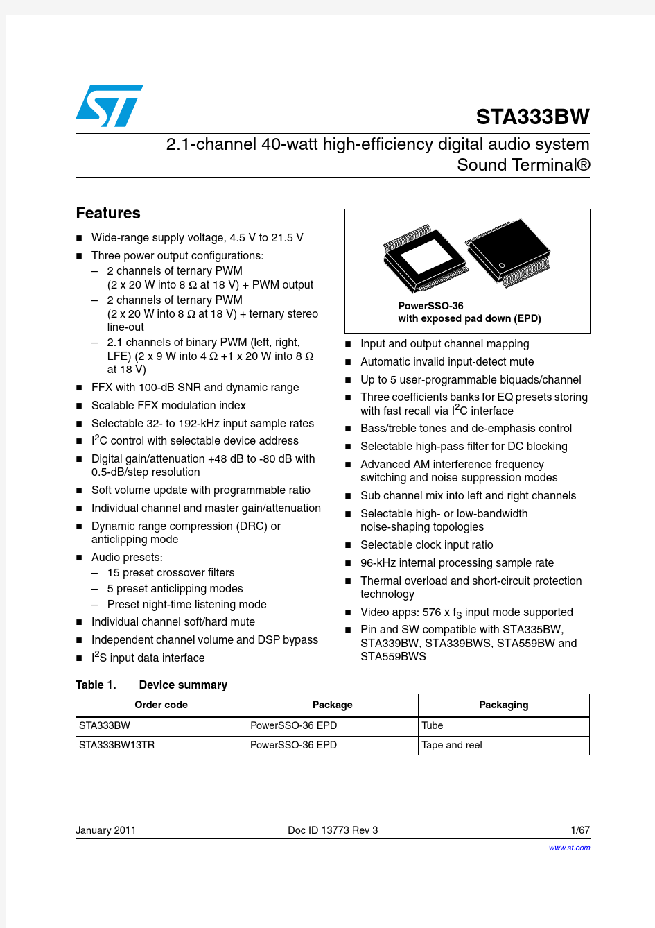
Table 1.
Device summary
Order code
Package
Packaging
ST A333BW PowerSSO-36 EPD Tube ST A333BW13TR
PowerSSO-36 EPD
Tape and reel
https://www.doczj.com/doc/4a5831215.html,
Contents STA333BW
Contents
1Description . . . . . . . . . . . . . . . . . . . . . . . . . . . . . . . . . . . . . . . . . . . . . . . . . 8
2Pin connections . . . . . . . . . . . . . . . . . . . . . . . . . . . . . . . . . . . . . . . . . . . . . 9
2.1Connection diagram . . . . . . . . . . . . . . . . . . . . . . . . . . . . . . . . . . . . . . . . . . 9
2.2Pin description . . . . . . . . . . . . . . . . . . . . . . . . . . . . . . . . . . . . . . . . . . . . . . 9
3Electrical specifications . . . . . . . . . . . . . . . . . . . . . . . . . . . . . . . . . . . . . 11
3.1Absolute maximum ratings . . . . . . . . . . . . . . . . . . . . . . . . . . . . . . . . . . . . 11
3.2Thermal data . . . . . . . . . . . . . . . . . . . . . . . . . . . . . . . . . . . . . . . . . . . . . . 11
3.3Recommended operating conditions . . . . . . . . . . . . . . . . . . . . . . . . . . . . 12
3.4Electrical specifications for the digital section . . . . . . . . . . . . . . . . . . . . . 12
3.5Electrical specifications for the power section . . . . . . . . . . . . . . . . . . . . . 13
3.6Power-on/off sequence . . . . . . . . . . . . . . . . . . . . . . . . . . . . . . . . . . . . . . . 15 4Processing data paths . . . . . . . . . . . . . . . . . . . . . . . . . . . . . . . . . . . . . . 16
5I2C bus specification . . . . . . . . . . . . . . . . . . . . . . . . . . . . . . . . . . . . . . . . 18
5.1Communication protocol . . . . . . . . . . . . . . . . . . . . . . . . . . . . . . . . . . . . . . 18
5.1.1Data transition or change . . . . . . . . . . . . . . . . . . . . . . . . . . . . . . . . . . . . 18
5.1.2Start condition . . . . . . . . . . . . . . . . . . . . . . . . . . . . . . . . . . . . . . . . . . . . 18
5.1.3Stop condition . . . . . . . . . . . . . . . . . . . . . . . . . . . . . . . . . . . . . . . . . . . . 18
5.1.4Data input . . . . . . . . . . . . . . . . . . . . . . . . . . . . . . . . . . . . . . . . . . . . . . . 18
5.2Device addressing . . . . . . . . . . . . . . . . . . . . . . . . . . . . . . . . . . . . . . . . . . 18
5.3Write operation . . . . . . . . . . . . . . . . . . . . . . . . . . . . . . . . . . . . . . . . . . . . . 19
5.3.1Byte write . . . . . . . . . . . . . . . . . . . . . . . . . . . . . . . . . . . . . . . . . . . . . . . . 19
5.3.2Multi-byte write . . . . . . . . . . . . . . . . . . . . . . . . . . . . . . . . . . . . . . . . . . . . 19
5.4Read operation . . . . . . . . . . . . . . . . . . . . . . . . . . . . . . . . . . . . . . . . . . . . . 19
5.4.1Current address byte read . . . . . . . . . . . . . . . . . . . . . . . . . . . . . . . . . . . 19
5.4.2Current address multi-byte read . . . . . . . . . . . . . . . . . . . . . . . . . . . . . . 19
5.4.3Random address byte read . . . . . . . . . . . . . . . . . . . . . . . . . . . . . . . . . . 19
5.4.4Random address multi-byte read . . . . . . . . . . . . . . . . . . . . . . . . . . . . . . 20 6Register description . . . . . . . . . . . . . . . . . . . . . . . . . . . . . . . . . . . . . . . . 21
2/67Doc ID 13773 Rev 3
STA333BW Contents
6.1Configuration registers (addr 0x00 to 0x05) . . . . . . . . . . . . . . . . . . . . . . . 22
6.1.1Configuration register A (addr 0x00) . . . . . . . . . . . . . . . . . . . . . . . . . . . 22
6.1.2Configuration register B (addr 0x01) . . . . . . . . . . . . . . . . . . . . . . . . . . . 24
6.1.3Configuration register C (addr 0x02) . . . . . . . . . . . . . . . . . . . . . . . . . . . 27
6.1.4Configuration register D (addr 0x03) . . . . . . . . . . . . . . . . . . . . . . . . . . . 29
6.1.5Configuration register E (addr 0x04) . . . . . . . . . . . . . . . . . . . . . . . . . . . 31
6.1.6Configuration register F (addr 0x05) . . . . . . . . . . . . . . . . . . . . . . . . . . . 32
6.2Volume control registers (addr 0x06 - 0x0A) . . . . . . . . . . . . . . . . . . . . . . 40
6.2.1Mute / line output configuration register (addr 0x06) . . . . . . . . . . . . . . . 41
6.2.2Master volume register (addr 0x07) . . . . . . . . . . . . . . . . . . . . . . . . . . . . 41
6.2.3Channel 1 volume (addr 0x08) . . . . . . . . . . . . . . . . . . . . . . . . . . . . . . . . 41
6.2.4Channel 2 volume (addr 0x09) . . . . . . . . . . . . . . . . . . . . . . . . . . . . . . . . 41
6.2.5Channel 3 / line output volume (addr 0x0A) . . . . . . . . . . . . . . . . . . . . . . 42
6.3Audio preset registers (addr 0x0B and 0x0C) . . . . . . . . . . . . . . . . . . . . . 43
6.3.1Audio preset register 1 (addr 0x0B) . . . . . . . . . . . . . . . . . . . . . . . . . . . . 43
6.3.2Audio preset register 2 (addr 0x0C) . . . . . . . . . . . . . . . . . . . . . . . . . . . . 43
6.4Channel configuration registers (addr 0x0E - 0x10) . . . . . . . . . . . . . . . . . 45
6.5Tone control register (addr 0x11) . . . . . . . . . . . . . . . . . . . . . . . . . . . . . . . 47
6.6Dynamic control registers (addr 0x12 - 0x15) . . . . . . . . . . . . . . . . . . . . . 47
6.6.1Limiter 1 attack / release rate (addr 0x12) . . . . . . . . . . . . . . . . . . . . . . . 47
6.6.2Limiter 1 attack / release threshold (addr 0x13) . . . . . . . . . . . . . . . . . . . 47
6.6.3Limiter 2 attack / release rate (addr 0x14) . . . . . . . . . . . . . . . . . . . . . . . 48
6.6.4Limiter 2 attack / release threshold (addr 0x15) . . . . . . . . . . . . . . . . . . . 48
6.6.5Description . . . . . . . . . . . . . . . . . . . . . . . . . . . . . . . . . . . . . . . . . . . . . . . 48
6.7User-defined coefficient control registers (addr 0x16 - 0x26) . . . . . . . . . . 53
6.7.1Coefficient address register (addr 0x16) . . . . . . . . . . . . . . . . . . . . . . . . 53
6.7.2Coefficient b1 data register bits (addr 0x17 - 0x19) . . . . . . . . . . . . . . . . 53
6.7.3Coefficient b2 data register bits (addr 0x1A - 0x1C) . . . . . . . . . . . . . . . 53
6.7.4Coefficient a1 data register bits (addr 0x1D - 0x1F) . . . . . . . . . . . . . . . 53
6.7.5Coefficient a2 data register bits (addr 0x20 - 0x22) . . . . . . . . . . . . . . . . 54
6.7.6Coefficient b0 data register bits (addr 0x23 - 0x25) . . . . . . . . . . . . . . . . 54
6.7.7Coefficient read / write control register (addr 0x26) . . . . . . . . . . . . . . . . 54
6.7.8Description . . . . . . . . . . . . . . . . . . . . . . . . . . . . . . . . . . . . . . . . . . . . . . . 55
6.8Variable max power correction registers (addr 0x27 - 0x28) . . . . . . . . . . 59
6.9Distortion compensation registers (addr 0x29 - 0x2A) . . . . . . . . . . . . . . . 59
6.10Fault detect recovery constant registers (addr 0x2B - 0x2C) . . . . . . . . . . 59
Doc ID 13773 Rev 33/67
Contents STA333BW
6.11Device status register (addr 0x2D) . . . . . . . . . . . . . . . . . . . . . . . . . . . . . . 60
7Applications . . . . . . . . . . . . . . . . . . . . . . . . . . . . . . . . . . . . . . . . . . . . . . . 61
7.1Applications schematic . . . . . . . . . . . . . . . . . . . . . . . . . . . . . . . . . . . . . . . 61
7.2PLL filter circuit . . . . . . . . . . . . . . . . . . . . . . . . . . . . . . . . . . . . . . . . . . . . . 61
7.3Typical output configuration . . . . . . . . . . . . . . . . . . . . . . . . . . . . . . . . . . . 61 8Package thermal characteristics . . . . . . . . . . . . . . . . . . . . . . . . . . . . . . 63 9Package mechanical data . . . . . . . . . . . . . . . . . . . . . . . . . . . . . . . . . . . . 64 10Revision history . . . . . . . . . . . . . . . . . . . . . . . . . . . . . . . . . . . . . . . . . . . 66
4/67Doc ID 13773 Rev 3
STA333BW List of figures List of figures
Figure 1.Block diagram . . . . . . . . . . . . . . . . . . . . . . . . . . . . . . . . . . . . . . . . . . . . . . . . . . . . . . . . . . . 8 Figure 2.Pin connection PowerSSO-36 (top view) . . . . . . . . . . . . . . . . . . . . . . . . . . . . . . . . . . . . . . . 9 Figure 3.Test circuit . . . . . . . . . . . . . . . . . . . . . . . . . . . . . . . . . . . . . . . . . . . . . . . . . . . . . . . . . . . . . 14 Figure 4.Power-on sequence . . . . . . . . . . . . . . . . . . . . . . . . . . . . . . . . . . . . . . . . . . . . . . . . . . . . . . 15 Figure 5.Power-off sequence for pop-free turn-off . . . . . . . . . . . . . . . . . . . . . . . . . . . . . . . . . . . . . . 15 Figure 6.Left and right processing, section 1 . . . . . . . . . . . . . . . . . . . . . . . . . . . . . . . . . . . . . . . . . . 16 Figure 7.Left and right processing, section 2 . . . . . . . . . . . . . . . . . . . . . . . . . . . . . . . . . . . . . . . . . . 17 Figure 8.Write mode sequence. . . . . . . . . . . . . . . . . . . . . . . . . . . . . . . . . . . . . . . . . . . . . . . . . . . . . 19 Figure 9.Read mode sequence. . . . . . . . . . . . . . . . . . . . . . . . . . . . . . . . . . . . . . . . . . . . . . . . . . . . . 20 Figure 10.OCFG = 00 (default value) . . . . . . . . . . . . . . . . . . . . . . . . . . . . . . . . . . . . . . . . . . . . . . . . . 34 Figure 11.OCFG = 01 . . . . . . . . . . . . . . . . . . . . . . . . . . . . . . . . . . . . . . . . . . . . . . . . . . . . . . . . . . . . 34 Figure 12.OCFG = 10 . . . . . . . . . . . . . . . . . . . . . . . . . . . . . . . . . . . . . . . . . . . . . . . . . . . . . . . . . . . . 34 Figure 13.OCFG = 11 . . . . . . . . . . . . . . . . . . . . . . . . . . . . . . . . . . . . . . . . . . . . . . . . . . . . . . . . . . . . 35 Figure 14.Output mapping scheme . . . . . . . . . . . . . . . . . . . . . . . . . . . . . . . . . . . . . . . . . . . . . . . . . . 35 Figure 15. 2.0 channels (OCFG = 00) PWM slots . . . . . . . . . . . . . . . . . . . . . . . . . . . . . . . . . . . . . . . 36 Figure 16. 2.1 channels (OCFG = 01) PWM slots . . . . . . . . . . . . . . . . . . . . . . . . . . . . . . . . . . . . . . . 37 Figure 17. 2.1 channels (OCFG = 10) PWM slots . . . . . . . . . . . . . . . . . . . . . . . . . . . . . . . . . . . . . . . 38 Figure 18.Basic limiter and volume flow diagram. . . . . . . . . . . . . . . . . . . . . . . . . . . . . . . . . . . . . . . . 48 Figure 19.Output configuration for stereo BTL mode (R L = 8?) . . . . . . . . . . . . . . . . . . . . . . . . . . . . 61 Figure 20.Applications circuit . . . . . . . . . . . . . . . . . . . . . . . . . . . . . . . . . . . . . . . . . . . . . . . . . . . . . . . 62 Figure 21.PowerSSO-36 power derating curve . . . . . . . . . . . . . . . . . . . . . . . . . . . . . . . . . . . . . . . . . 63 Figure 22.PowerSSO-36 EPD outline drawing . . . . . . . . . . . . . . . . . . . . . . . . . . . . . . . . . . . . . . . . . 65
Doc ID 13773 Rev 35/67
List of tables STA333BW List of tables
Table 1.Device summary. . . . . . . . . . . . . . . . . . . . . . . . . . . . . . . . . . . . . . . . . . . . . . . . . . . . . . . . . . 1 Table 2.Pin description . . . . . . . . . . . . . . . . . . . . . . . . . . . . . . . . . . . . . . . . . . . . . . . . . . . . . . . . . . . 9 Table 3.Absolute maximum ratings. . . . . . . . . . . . . . . . . . . . . . . . . . . . . . . . . . . . . . . . . . . . . . . . . 11 Table 4.Thermal data. . . . . . . . . . . . . . . . . . . . . . . . . . . . . . . . . . . . . . . . . . . . . . . . . . . . . . . . . . . . 11 Table 5.Recommended operating condition . . . . . . . . . . . . . . . . . . . . . . . . . . . . . . . . . . . . . . . . . . 12 Table 6.Electrical specifications - digital section . . . . . . . . . . . . . . . . . . . . . . . . . . . . . . . . . . . . . . . 12 Table 7.Electrical specifications - power section. . . . . . . . . . . . . . . . . . . . . . . . . . . . . . . . . . . . . . . 13 Table 8.Register summary. . . . . . . . . . . . . . . . . . . . . . . . . . . . . . . . . . . . . . . . . . . . . . . . . . . . . . . . 21 Table 9.Master clock select. . . . . . . . . . . . . . . . . . . . . . . . . . . . . . . . . . . . . . . . . . . . . . . . . . . . . . . 22 Table 10.Input sampling rates. . . . . . . . . . . . . . . . . . . . . . . . . . . . . . . . . . . . . . . . . . . . . . . . . . . . . . 23 Table 11.Internal interpolation ratio. . . . . . . . . . . . . . . . . . . . . . . . . . . . . . . . . . . . . . . . . . . . . . . . . . 23 Table 12.IR bit settings as a function of input sample rate . . . . . . . . . . . . . . . . . . . . . . . . . . . . . . . . 23 Table 13.Thermal warning recovery bypass . . . . . . . . . . . . . . . . . . . . . . . . . . . . . . . . . . . . . . . . . . . 24 Table 14.Thermal warning adjustment bypass . . . . . . . . . . . . . . . . . . . . . . . . . . . . . . . . . . . . . . . . . 24 Table 15.Fault detect recovery bypass . . . . . . . . . . . . . . . . . . . . . . . . . . . . . . . . . . . . . . . . . . . . . . . 24 Table 16.Serial audio input interface. . . . . . . . . . . . . . . . . . . . . . . . . . . . . . . . . . . . . . . . . . . . . . . . . 25 Table 17.Serial data first bit. . . . . . . . . . . . . . . . . . . . . . . . . . . . . . . . . . . . . . . . . . . . . . . . . . . . . . . . 25 Table 18.Support serial audio input formats for MSB-first (SAIFB = 0). . . . . . . . . . . . . . . . . . . . . . . 25 Table 19.Supported serial audio input formats for LSB-first (SAIFB = 1) . . . . . . . . . . . . . . . . . . . . . 26 Table 20.Delay serial clock enable . . . . . . . . . . . . . . . . . . . . . . . . . . . . . . . . . . . . . . . . . . . . . . . . . . 27 Table 21.Channel input mapping. . . . . . . . . . . . . . . . . . . . . . . . . . . . . . . . . . . . . . . . . . . . . . . . . . . . 27 Table 22.FFX power output mode. . . . . . . . . . . . . . . . . . . . . . . . . . . . . . . . . . . . . . . . . . . . . . . . . . . 28 Table 23.FFX compensating pulse size bits . . . . . . . . . . . . . . . . . . . . . . . . . . . . . . . . . . . . . . . . . . . 28 Table https://www.doczj.com/doc/4a5831215.html,pensating pulse size . . . . . . . . . . . . . . . . . . . . . . . . . . . . . . . . . . . . . . . . . . . . . . . . . . 28 Table 25.Overcurrent warning bypass. . . . . . . . . . . . . . . . . . . . . . . . . . . . . . . . . . . . . . . . . . . . . . . . 28 Table 26.High-pass filter bypass. . . . . . . . . . . . . . . . . . . . . . . . . . . . . . . . . . . . . . . . . . . . . . . . . . . . 29 Table 27.De-emphasis. . . . . . . . . . . . . . . . . . . . . . . . . . . . . . . . . . . . . . . . . . . . . . . . . . . . . . . . . . . . 29 Table 28.DSP bypass . . . . . . . . . . . . . . . . . . . . . . . . . . . . . . . . . . . . . . . . . . . . . . . . . . . . . . . . . . . . 29 Table 29.Postscale link . . . . . . . . . . . . . . . . . . . . . . . . . . . . . . . . . . . . . . . . . . . . . . . . . . . . . . . . . . . 29 Table 30.Biquad coefficient link. . . . . . . . . . . . . . . . . . . . . . . . . . . . . . . . . . . . . . . . . . . . . . . . . . . . . 30 Table 31.Dynamic range compression / anticlipping bit . . . . . . . . . . . . . . . . . . . . . . . . . . . . . . . . . . 30 Table 32.Zero-detect mute enable. . . . . . . . . . . . . . . . . . . . . . . . . . . . . . . . . . . . . . . . . . . . . . . . . . . 30 Table 33.Submix mode enable . . . . . . . . . . . . . . . . . . . . . . . . . . . . . . . . . . . . . . . . . . . . . . . . . . . . . 30 Table 34.Max power correction variable . . . . . . . . . . . . . . . . . . . . . . . . . . . . . . . . . . . . . . . . . . . . . . 31 Table 35.Max power correction. . . . . . . . . . . . . . . . . . . . . . . . . . . . . . . . . . . . . . . . . . . . . . . . . . . . . 31 Table 36.Noise-shaper bandwidth selection . . . . . . . . . . . . . . . . . . . . . . . . . . . . . . . . . . . . . . . . . . . 31 Table 37.AM mode enable. . . . . . . . . . . . . . . . . . . . . . . . . . . . . . . . . . . . . . . . . . . . . . . . . . . . . . . . . 31 Table 38.PWM speed mode . . . . . . . . . . . . . . . . . . . . . . . . . . . . . . . . . . . . . . . . . . . . . . . . . . . . . . . 32 Table 39.Distortion compensation variable enable . . . . . . . . . . . . . . . . . . . . . . . . . . . . . . . . . . . . . . 32 Table 40.Zero-crossing volume enable. . . . . . . . . . . . . . . . . . . . . . . . . . . . . . . . . . . . . . . . . . . . . . . 32 Table 41.Soft volume update enable. . . . . . . . . . . . . . . . . . . . . . . . . . . . . . . . . . . . . . . . . . . . . . . . . 32 Table 42.Output configuration. . . . . . . . . . . . . . . . . . . . . . . . . . . . . . . . . . . . . . . . . . . . . . . . . . . . . . 33 Table 43.Output configuration engine selection . . . . . . . . . . . . . . . . . . . . . . . . . . . . . . . . . . . . . . . . 33 Table 44.Invalid input detect mute enable. . . . . . . . . . . . . . . . . . . . . . . . . . . . . . . . . . . . . . . . . . . . . 39 Table 45.Binary output mode clock loss detection . . . . . . . . . . . . . . . . . . . . . . . . . . . . . . . . . . . . . . 39 Table 46.LRCK double trigger protection . . . . . . . . . . . . . . . . . . . . . . . . . . . . . . . . . . . . . . . . . . . . . 39 Table 47.Auto EAPD on clock loss . . . . . . . . . . . . . . . . . . . . . . . . . . . . . . . . . . . . . . . . . . . . . . . . . . 39 Table 48.IC power down . . . . . . . . . . . . . . . . . . . . . . . . . . . . . . . . . . . . . . . . . . . . . . . . . . . . . . . . . . 39 6/67Doc ID 13773 Rev 3
STA333BW List of tables Table 49.External amplifier power down . . . . . . . . . . . . . . . . . . . . . . . . . . . . . . . . . . . . . . . . . . . . . . 40 Table 50.Line output configuration . . . . . . . . . . . . . . . . . . . . . . . . . . . . . . . . . . . . . . . . . . . . . . . . . . 41 Table 51.Master volume offset as a function of MVOL . . . . . . . . . . . . . . . . . . . . . . . . . . . . . . . . . . . 41 Table 52.Channel volume as a function of CxVOL . . . . . . . . . . . . . . . . . . . . . . . . . . . . . . . . . . . . . . 42 Table 53.Audio preset gain compression / limiters selection for AMGC[3:2] = 00. . . . . . . . . . . . . . . 43 Table 54.AM interference frequency switching bits. . . . . . . . . . . . . . . . . . . . . . . . . . . . . . . . . . . . . . 43 Table 55.Audio preset AM switching frequency selection. . . . . . . . . . . . . . . . . . . . . . . . . . . . . . . . . 43 Table 56.Bass management crossover. . . . . . . . . . . . . . . . . . . . . . . . . . . . . . . . . . . . . . . . . . . . . . . 44 Table 57.Bass management crossover frequency . . . . . . . . . . . . . . . . . . . . . . . . . . . . . . . . . . . . . . 44 Table 58.Tone control bypass. . . . . . . . . . . . . . . . . . . . . . . . . . . . . . . . . . . . . . . . . . . . . . . . . . . . . . 45 Table 59.EQ bypass . . . . . . . . . . . . . . . . . . . . . . . . . . . . . . . . . . . . . . . . . . . . . . . . . . . . . . . . . . . . . 45 Table 60.Volume bypass register . . . . . . . . . . . . . . . . . . . . . . . . . . . . . . . . . . . . . . . . . . . . . . . . . . . 45 Table 61.Binary output enable registers . . . . . . . . . . . . . . . . . . . . . . . . . . . . . . . . . . . . . . . . . . . . . . 46 Table 62.Channel limiter mapping as a function of CxLS bits. . . . . . . . . . . . . . . . . . . . . . . . . . . . . . 46 Table 63.Channel output mapping as a function of CxOM bits. . . . . . . . . . . . . . . . . . . . . . . . . . . . . 46 Table 64.Tone control boost / cut as a function of BTC and TTC bits. . . . . . . . . . . . . . . . . . . . . . . . 47 Table 65.Limiter attack rate vs LxA bits. . . . . . . . . . . . . . . . . . . . . . . . . . . . . . . . . . . . . . . . . . . . . . . 49 Table 66.Limiter release rate vs LxR bits . . . . . . . . . . . . . . . . . . . . . . . . . . . . . . . . . . . . . . . . . . . . . 50 Table 67.Limiter attack threshold vs LxAT bits (AC mode) . . . . . . . . . . . . . . . . . . . . . . . . . . . . . . . . 50 Table 68.Limiter release threshold vs LxRT bits (AC mode). . . . . . . . . . . . . . . . . . . . . . . . . . . . . . . 51 Table 69.Limiter attack threshold vs LxAT bits (DRC mode). . . . . . . . . . . . . . . . . . . . . . . . . . . . . . . 51 Table 70.Limiter release threshold vs LxRT bits (DRC mode). . . . . . . . . . . . . . . . . . . . . . . . . . . . . . 52 Table 71.RAM block for biquads, mixing, scaling, bass management. . . . . . . . . . . . . . . . . . . . . . . . 56 Table 72.Status register bits . . . . . . . . . . . . . . . . . . . . . . . . . . . . . . . . . . . . . . . . . . . . . . . . . . . . . . . 60 Table 73.PowerSSO-36 EPD dimensions. . . . . . . . . . . . . . . . . . . . . . . . . . . . . . . . . . . . . . . . . . . . . 64 Table 74.Document revision history . . . . . . . . . . . . . . . . . . . . . . . . . . . . . . . . . . . . . . . . . . . . . . . . . 66
Doc ID 13773 Rev 37/67
Description STA333BW
8/67Doc ID 13773 Rev 3
1 Description
The STA333BW is an integrated solution of digital audio processing, digital amplifier
controls and power output stages to create a high-power single-chip FFX digital amplifier with high-quality and high-efficiency. Three channels of FFX processing are provided. The FFX processor implements the ternary, binary and binary differential processing capabilities of the full FFX processor.
The STA333BW is part of the Sound Terminal ? family that provides full digital audio
streaming to the speakers and offers cost effectiveness, low power dissipation and sound enrichment.
The power section consists of four independent half-bridges. These can be configured via digital control to operate in different modes.
For example, 2.1 channels can be provided by two half-bridges and a single full-bridge, supplying up to 2 x 9 W + 1 x 20 W of output power or two channels can be provided by two full-bridges, supplying up to 2 x 20 W of output power.
The IC can also be configured as 2.1 channels with 2 x 20 W supplied by the device plus a drive for an external FFX power amplifier, such as STA533WF or STA515W.
The serial audio data input interface accepts all possible formats, including the popular I 2S format. The high-quality conversion from PCM audio to FFX PWM switching provides over 100dB of SNR and of dynamic range.
Also provided in the ST A333BW are a full assortment of digital processing features. This includes up to 5 programmable biquads (EQ) per channel. Available presets enable a time-to-market advantage by substantially reducing the amount of software development needed for functions such as audio preset volume loudness, preset volume curves and preset EQ settings. There are also new advanced AM radio interference reduction modes. The DRC dynamically equalizes the system to provide a linear frequency speaker response regardless of output power level.Figure 1.
Block diagram
Protection current / thermal
Logic
Regulators
Bias
Power control
FFX
PLL
Volume control
Channel 1A
Channel 1B
Channel 2A
Channel 2B
I 2S interface
Power
Digital DSP
I 2C
STA333BW Pin connections
Doc ID 13773 Rev 39/67
2 Pin connections
2.1 Connection diagram
Figure 2.
Pin connection PowerSSO-36 (top view)
2.2 Pin description
123456789101112131415161718
363534333231302928272625242322212019
VDD_DIG GND_DIG SCL SDA INT_LINE RESET SDI LRCKI BICKI XTI GND_PLL FILTER_PLL VDD_PLL PWRDN GND_DIG VDD_DIG TWARN / OUT4A EAPD / OUT4B
GND_SUB
SA
TEST_MODE
VSS VCC_REG OUT2B GND2VCC2OUT2A OUT1B VCC1GND1OUT1A GND_REG
VDD CONFIG
OUT3B / FFX3B OUT3A / FFX3A
D05AU1638
EP , exposed pad
(device ground)
Table 2.
Pin description
Pin Type Name Description
1GND GND_SUB Substrate ground
2I SA
I 2C select address (pull-down)
3I TEST_MODE This pin must be connected to ground (pull-down)4I/O VSS Internal reference at V CC - 3.3V 5I/O VCC_REG Internal V CC reference 6O OUT2B Output half-bridge channel 2B 7GND GND2Power negative supply 8Power VCC2Power positive supply 9O OUT2A Output half-bridge channel 2A 10
O
OUT1B
Output half-bridge channel 1B
Pin connections
STA333BW
10/67Doc ID 13773 Rev 3
11Power VCC1Power positive supply 12GND GND1Power negative supply 13O OUT1A Output half-bridge channel 1A 14GND GND_REG Internal ground reference 15Power VDD Internal 3.3V reference voltage 16I CONFIG Parallel mode command
17O OUT3B / FFX3B PWM out channel 3B / external bridge driver 18O OUT3A / FFX3A PWM out channel 3A / external bridge driver
19O EAPD / OUT4B Power down for external bridge / PWM out channel 4B 20I/O TWARN / OUT4A Thermal warning from external bridge (pull-up when input) / PWM out channel 4A 21Power VDD_DIG Digital supply voltage 22GND GND_DIG Digital ground 23I PWRDN Power down (pull-up)24Power VDD_PLL Positive supply for PLL 25I FILTER_PLL Connection to PLL filter 26GND GND_PLL Negative supply for PLL 27I XTI PLL input clock 28I BICKI I 2S serial clock 29I LRCKI I 2S left / right clock
30I SDI I 2S serial data channels 1 and 231I RESET Reset (pull-up)32O INT_LINE Fault interrupt 33I/O SDA I 2C serial data 34I SCL I 2C serial clock 35GND GND_DIG Digital ground 36Power VDD_DIG Digital supply voltage
-
-EP
Exposed pad for PCB heatsink, to be connected to GND
Table 2.
Pin description (continued)
Pin Type Name
Description
STA333BW Electrical specifications
Doc ID 13773 Rev 311/67
3 Electrical specifications
3.1
Absolute maximum ratings
Warning:
Stresses beyond those listed in Table 3 above may cause
permanent damage to the device. These are stress ratings only, and functional operation of the device at these or any other conditions beyond those indicated under
“Recommended operating conditions” are not implied. Exposure to absolute-maximum-rated conditions for extended periods may affect device reliability. In the real
application, power supplies with nominal values rated within the recommended operating conditions, may experience some rising beyond the maximum operating conditions for a short time when no or very low current is sinked (amplifier in mute state). In this case the reliability of the device is
guaranteed, provided that the absolute maximum ratings are not exceeded.
3.2 Thermal data
Table 3.
Absolute maximum ratings
Symbol Parameter Min Typ Max Unit V CC Power supply voltage (pins VCCx) -0.3-24 V V DD Digital supply voltage (pins VDD_DIG)-0.3 - 4.0V V DD PLL supply voltage (pin VDD_PLL)-0.3- 4.0V T op
Operating junction temperature
-20
-150
°C
T stg Storage
temperature -40 -150 °C
Table 4.
Thermal data
Parameter
Min Typ
Max Unit R th j-case Thermal resistance junction-case (thermal pad)- - 1.5°C/W T th-sdj Thermal shut-down junction temperature -150-°C T th-w Thermal warning temperature -130-°C T th-sdh Thermal shut-down hysteresis
-20-°C R th j-amb
Thermal resistance junction-ambient (1)
1.See Chapter 8: Package thermal characteristics on page 63 for details.
-24-°C/W
Electrical specifications STA333BW
12/67Doc ID 13773 Rev 3
3.3 Recommended operating conditions
3.4 Electrical specifications for the digital section
The specifications given in this section are valid for T amb = 25 °C unless otherwise specified.
Table 5.
Recommended operating condition
Symbol Parameter Min Typ Max Unit V CC Power supply voltage (VCCxA, VCCxB) 4.5
-21.5
V
V DD_DIG D
igital supply voltage 2.7 3.3 3.6 V V DD_PLL
PLL supply voltage
2.7
3.3 3.6
V
T amb Ambient
temperature -20
-70 °C
Table 6.
Electrical specifications - digital section
Symbol Parameter Conditions Min Typ Max Unit I il Low level input current without
pull-up/down device
Vi = 0 V
--1
μA I ih High level input current without pull-up/down device Vi = VDD_DIG =3.6 V --1
μA V il Low level input voltage ---0.2*
VDD_DIG
V V ih
High level input voltage
-
0.8*
VDD_DIG
--V V ol Low level output voltage Iol = 2 mA -0.4*
VDD_DIG
V V oh High level output voltage Ioh = 2 mA 0.8*
VDD_DIG
--V R pu
Equivalent pull-up/down
resistance
--
50
-
k ?
STA333BW Electrical specifications
Doc ID 13773 Rev 313/67
3.5 Electrical specifications for the power section
The specifications given in this section are valid for the operating conditions: V CC =18V ,
f =1kHz, f sw = 384kHz, T amb = 25°C and R L = 8?, unless otherwise specified.
Table 7.
Electrical specifications - power section
Symbol
Parameter Conditions
Min Typ Max Unit
Po
Output power BTL
THD = 1%-16-W
THD = 10%-20-Output power SE
THD = 1%, R L = 4?
-
7-W THD = 10%, R L = 4?-9-R dsON Power P-channel or N-channel MOSFET l d = 0.75A --250 m ? gP Power P-channel R dsON matching l d = 0.75A -100-%gN Power N-channel R dsON matching l d = 0.75A -100-%Idss Power P-channel / N-channel leakage V CC = 20 V --1
μA
t r Rise time Resistive load,
see Figure 3 below --10 ns t f Fall time
--10 ns I VCC Supply current from V CC in power down PWRDN = 0 -0.3-μA Supply current from V CC in operation PWRDN = 1-15-mA I VDD Supply current FFX processing Internal clock = 49.152 MHz
-55-mA I LIM Overcurrent limit (1)
2.2
3.0
- A I SCP Short -circuit protection R L = 0? 2.7 3.6- A V UVP Undervoltage protection --- 4.3 V t min Output minimum pulse width No load 20 40 60 ns DR Dynamic range
--100-dB SNR
Signal to noise ratio, ternary mode A-Weighted -100-dB Signal to noise ratio binary mode --90-dB THD+N
T otal harmonic distortion + noise
FFX stereo mode, Po =1W f =1kHz
-0.2
-%
X TALK
Crosstalk
FFX stereo mode, <5kHz
One channel driven at 1W, other channel measured -80-dB
η
Peak efficiency, FFX mode
Po = 2 x 20W into 8?
-
90-%
Peak efficiency, binary modes
Po = 2 x 9W into 4?
+ 1 x 20W into 8?
-87
-
1.Limit the current if overcurrent warning detect adjustment bypass is enabled (register bit CONFC.OCRB on
page 28). When disabled refer to the I SCP .
Electrical specifications STA333BW
14/67Doc ID 13773 Rev 3
STA333BW Electrical specifications
Doc ID 13773 Rev 315/67
3.6 Power-on/off sequence
Note:
The definition of a stable clock is when f max - f min < 1 MHz.
Section Serial audio input interface format on page 25 gives information on setting up the I 2S interface.
Processing data paths STA333BW 4 Processing data paths
Figure6 and Figure7 below show the data processing paths inside STA333BW. The whole
processing chain is composed of two consecutive sections. In the first one, dual-channel
processing is implemented and in the second section each channel is fed into the post
mixing block either to generate a third channel (typically used in 2.1 output configuration and
with crossover filters enabled) or to have the channels processed by the DRC block (2.0
output configuration with crossover filters used to define the cut-off frequency of the two
bands).
The first section, Figure6, begins with a 2x oversampling FIR filter providing 2 * f S audio
processing. Then a selectable high-pass filter removes the DC level (enabled if HPB=0).
The left and right channel processing paths can include up to 8 filters, depending on the
selected configuration (bits BQL, BQ5, BQ6, BQ7 and XO[3:0]). By default, four user
programmable, independent filters per channel are enabled, plus the preconfigured
de-emphasis, bass and treble controls (BQL = 0, BQ5 = 0, BQ6 = 0, BQ7 = 0).
If the coefficient sets for the two channels are linked (BQL = 1) it is possible to use the
de-emphasis, bass and treble filters in a user defined configuration (provided the relevant
BQx bits are set). In this case both channels use the same processing coefficients and can
have up to seven filters each. If BQL = 0 the BQx bits are ignored and the fifth, sixth and
seventh filters are configured as de-emphasis, bass and treble controls, respectively.
Moreover, the common 8th filter can be available on both channels provided the predefined
crossover frequencies are not used, XO[3:0] = 0, and the DRC is not used.
In the second section, Figure7, mixing and crossover filters are available. If DRC is not
enabled they are fully user-programmable and allow the generation of a third channel
(2.1outputs). Alternatively, in mode DRC, these blocks are used to split the sub-band and
define the cut-off frequencies of the two bands. A prescaler and a final postscaler allow full
control over the signal dynamics before and after the filtering stages. A mixer function is also
available.
16/67Doc ID 13773 Rev 3
STA333BW Processing data paths
Doc ID 13773 Rev 317/67
I 2C bus specification
STA333BW
18/67Doc ID 13773 Rev 3
5 I
2C bus specification
The STA333BW supports the I 2C protocol via the input ports SCL and SDA_IN (master to slave) and the output port SDA_OUT (slave to master). This protocol defines any device that sends data on to the bus as a transmitter and any device that reads the data as a receiver. The device that controls the data transfer is known as the master and the other as the slave. The master always starts the transfer and provides the serial clock for synchronization. The STA333BW is always a slave device in all of its communications. It supports up to 400kb/s (fast-mode bit rate).
For correct operation of the I 2C interface ensure that the master clock generated by the PLL has a frequency at least 10 times higher than the frequency of the applied SCL clock.
5.1 Communication protocol
5.1.1
Data transition or change
Data changes on the SDA line must only occur when the clock SCL is low. A SDA transition
while the clock is high is used to identify a START or STOP condition.
5.1.2 Start condition
START is identified by a high to low transition of the data bus, SDA, while the clock, SCL, is
stable in the high state. A START condition must precede any command for data transfer.
5.1.3 Stop condition
STOP is identified by low to high transition of SDA while SCL is stable in the high state. A
STOP condition terminates communication between STA333BW and the bus master.
5.1.4 Data input
During the data input the STA333BW samples the SDA signal on the rising edge of SCL. For
correct device operation the SDA signal must be stable during the rising edge of the clock and the data can change only when the SCL line is low.
5.2 Device addressing
To start communication between the master and the STA333BW, the master must initiate
with a start condition. Following this, the master sends onto the SDA line 8-bits (MSB first) corresponding to the device select address and read or write mode bit.
The seven most significant bits are the device address identifiers, corresponding to the I 2C bus definition. In the STA333BW the I 2C interface has two device addresses depending on the SA pin configuration, 0x38 when SA = 0, and 0x3A when SA = 1.
The eighth bit (LSB) identifies a read or write operation (R/W); this is set to 1 for read and to 0 for write. After a ST ART condition the ST A333BW identifies the device address on the SDA bus and if a match is found, acknowledges the identification during the 9th bit time frame. The byte following the device identification is the address of a device register.
STA333BW
I 2C bus specification
Doc ID 13773 Rev 319/67
5.3 Write operation
Following the START condition the master sends a device select code with the RW bit set
to 0. The ST A333BW acknowledges this and then waits for the byte of internal address. After receiving the internal byte address the STA333BW again responds with an acknowledgement.
5.3.1 Byte write
In the byte write mode the master sends one data byte, this is acknowledged by the
STA333BW. The master then terminates the transfer by generating a STOP condition.
5.3.2 Multi-byte write
The multi-byte write modes can start from any internal address. The master generating a
STOP condition terminates the transfer.
5.4 Read operation
5.4.1
Current address byte read
Following the START condition the master sends a device select code with the RW bit set
to 1. The ST A333BW acknowledges this and then responds by sending one byte of data. The master then terminates the transfer by generating a STOP condition.
5.4.2 Current address multi-byte read
The multi-byte read modes can start from any internal address. Sequential data bytes are read from sequential addresses within the STA333BW. The master acknowledges each data byte read and then generates a STOP condition terminating the transfer.
5.4.3 Random address byte read
Following the START condition the master sends a device select code with the RW bit set
to 0. The ST A333BW acknowledges this and then the master writes the internal address byte. After receiving, the internal byte address the STA333BW again responds with an
acknowledgement. The master then initiates another ST ART condition and sends the device select code with the RW bit set to 1. The ST A333BW acknowledges this and then responds by sending one byte of data. The master then terminates the transfer by generating a STOP condition.
I2C bus specification STA333BW
5.4.4 Random address multi-byte read
The multi-byte read modes could start from any internal address. Sequential data bytes are
read from sequential addresses within the STA333BW. The master acknowledges each
data byte read and then generates a STOP condition terminating the transfer.
20/67Doc ID 13773 Rev 3
如何看懂电路图1--学电子跟我来系列文章 电子设备中有各种各样的图。能够说明它们工作原理的是电原理图,简称电路图。 电路图有两种,一种是说明模拟电子电路工作原理的。它用各种图形符号表示电阻器、电容器、开关、晶体管等实物,用线条把元器件和单元电路按工作原理的关系连接起来。这种图长期以来就一直被叫做电路图。 另一种是说明数字电子电路工作原理的。它用各种图形符号表示门、触发器和各种逻辑部件,用线条把它们按逻辑关系连接起来,它是用来说明各个逻辑单元之间的逻辑关系和整机的逻辑功能的。为了和模拟电路的电路图区别开来,就把这种图叫做逻辑电路图,简称逻辑图。 除了这两种图外,常用的还有方框图。它用一个框表示电路的一部分,它能简洁明了地说明电路各部分的关系和整机的工作原理。 一张电路图就好象是一篇文章,各种单元电路就好比是句子,而各种元器件就是组成句子的单词。所以要想看懂电路图,还得从认识单词——元器件开始。有关电阻器、电容器、电感线圈、晶体管等元器件的用途、类别、使用方法等内容可以点击本文相关文章下的各个链接,本文只把电路图中常出现的各种符号重述一遍,希望初学者熟悉它们,并记住不忘。 电阻器与电位器 符号详见图 1 所示,其中( a )表示一般的阻值固定的电阻器,( b )表示半可调或微调电阻器;( c )表示电位器;( d )表示带开关的电位器。电阻器的文字符号是“ R ”,电位器是“ RP ”,即在 R 的后面再加一个说明它有调节功能的字符“ P ”。 在某些电路中,对电阻器的功率有一定要求,可分别用图 1 中( e )、( f )、
( g )、( h )所示符号来表示。 几种特殊电阻器的符号: 第 1 种是热敏电阻符号,热敏电阻器的电阻值是随外界温度而变化的。有的是负温度系数的,用NTC来表示;有的是正温度系数的,用PTC来表示。它的符号见图( i ),用θ或t° 来表示温度。它的文字符号是“ RT ”。 第 2 种是光敏电阻器符号,见图 1 ( j ),有两个斜向的箭头表示光线。它的文字符号是“ RL ”。 第 3 种是压敏电阻器的符号。压敏电阻阻值是随电阻器两端所加的电压而变化的。符号见图 1 ( k ),用字符 U 表示电压。它的文字符号是“ RV ”。这三种电阻器实际上都是半导体器件,但习惯上我们仍把它们当作电阻器。 第 4 种特殊电阻器符号是表示新近出现的保险电阻,它兼有电阻器和熔丝的作用。当温度超过500℃ 时,电阻层迅速剥落熔断,把电路切断,能起到保护电路的作用。它的电阻值很小,目前在彩电中用得很多。它的图形符号见图 1 ( 1 ),文字符号是“ R F ”。 电容器的符号 详见图2 所示,其中( a )表示容量固定的电容器,( b )表示有极性电容器,例如各种电解电容器,( c )表示容量可调的可变电容器。( d )表示微调电容器,( e )表示一个双连可变电容器。电容器的文字符号是 C 。 电感器与变压器的符号 电感线圈在电路图中的图形符号见图 3 。其中( a )是电感线圈的一般符号,( b )是带磁芯或铁芯的线圈,( c )是铁芯有间隙的线圈,( d )是带可调磁芯的可调电感,( e )是有多个抽头的电感线圈。电感线圈的文字符号是“ L ”。
电路实验心得体会 电路实验,作为一门实实在在的实验学科,是电路知识的基础和依据。它可以帮助我们进一步理解巩固电路学的知识,激发我们对电路的学习兴趣。在大一上学期将要结束之际,我们进行了一系列的电路实验,从简单的戴维南定理到示波器的使用,再到回转路-----,一共五个实验,通过这五个实验,我对电路实验有了更深刻的了解,体会到了电路的神奇与奥妙。 不过说实话在做这次试验之前,我以为不会难做,就像以前做的实验一样,操作应该不会很难,做完实验之后两下子就将实验报告写完,直到做完这次电路实验时,我才知道其实并不容易做。它真的不像我想象中的那么简单,天真的以为自己把平时的理论课学好就可以很顺利的完成实验,事实证明我错了,当我走上试验台,我意识到要想以优秀的成绩完成此次所有的实验,难度很大,但我知道这个难度是与学到的知识成正比的,因此我想说,虽然我在实验的过程中遇到了不少困难,但最后的成绩还是不错的,因为我毕竟在这次实验中学到了许多在课堂上学不到的东西,终究使我在这次实验中受益匪浅。 下面我想谈谈我在所做的实验中的心得体会: 在基尔霍夫定律和叠加定理的验证实验中,进一步学习了基尔霍夫定律和叠加定理的应用,根据所画原理图,连接好实际电路,测量出实验数据,经计算实验结果均在误差范围内,说明该实验做的成功。我认为这两个实验的实验原理还是比较简单的,但实际操作起来并不是很简单,至少我觉得那些行行色色的导线就足以把你绕花眼,所以我想说这个实验不仅仅是对你所学知识掌握情况的考察,更是对你的耐心和眼力的一种考验。 在戴维南定理的验证实验中,了解到对于任何一个线性有源网络,总可以用一个电压源与一个电阻的串联来等效代替此电压源的电动势Us等于这个有源二端网络的开路电压Uoc,其等效内阻Ro等于该网络中所有独立源均置零时的等效电阻。这就是戴维南定理的具体说明,我认为其实质也就是在阐述一个等效的概念,我想无论你是学习理论知识还是进行实际操作,只要抓住这个中心,我想可能你所遇到的续都问题就可以迎刃而解。不过在做这个实验,我想我们应该注意一下万用表的使用,尽管它的操作很简单,但如果你马虎大意也是完全有可能出错的,是你整个的实验前功尽弃! 在接下来的常用电子仪器使用实验中,我们选择了对示波器的使用,我们通过了解示波器的原理,初步学会了示波器的使用方法。在试验中我们观察到了在不同频率、不同振幅下的各种波形,并且通过毫伏表得出了在不同情况下毫伏表的读数。 我们最后一个实验做的是一阶动态电路的研究,在这个实验中我们需要测定RL一阶电路的零输入响应,零状态响应以及全响应,学习电路时间常数的测量方法。因为动态网络的过渡过程是十分短暂的单次变化过程,如果我们选择用普通示波器过渡过程和测量有关的参数,我们就必须是这种单次变化的过程重复出现。因此我们利用信号发生器输出的
《电路理论》试卷 考试形式:闭卷考试 姓名:学号:专业层次:学习中心: 试卷说明: 1.考试时间为90分钟,请掌握好答题时间; 2.答题之前,请将试卷上的姓名、学号、专业层次和学习中心填写清楚; 3.本试卷所有试题答案写在答题卷上; 4.答题完毕,请将试卷和答题卷展开、正面向上交回,不得带出考场; 5.考试中心提示:请遵守考场纪律,参与公平竞争! 第一部分客观题部分 一、单项选择题(本大题共10小题,每小题2分,共20分) 1.电阻与电感元件并联,它们的电流有效值分别为3A 和4A,则它们总的电流有效值为( C )。 A.7A B.6A C.5A D.4A 2.关于理想电感元件的伏安关系,下列各式正确的有( D )。 A.u=ωLi B.u=Li C.u=jωLi D.u=Ldi/dt 3.应用叠加定理时,理想电流源不作用时视为( B )。 A.短路B.开路C.电阻D.理想电流源 4.在正弦交流电路中提高感性负载功率因数的方法是( D )。 A.负载串联电感B.负载串联电容C.负载并联电感D.负载并联电容5.任意一个相量乘以j相当于该相量( A )。 A.逆时针旋转90度B.顺时针旋转90度C.逆时针旋转60度D.顺时针旋转60度6.如图1-2所示,i=2A,u=30V,则元件的功率大小和对此二端电路的描述正确的是( B ) 图1-2 A.P=15W,吸收功率B.P=60W,吸收功率 C.P=15W,放出功率D.P=60W,放出功率 7.三相对称电源星型联结,相、线电压的关系为( A )。 A.线电压是相电压的3倍,且线电压滞后对应相电压30°
B .相电压是线电压的31 倍,且相电压滞后对应线电压30° C .线电压是相电压的2倍,且线电压滞后对应相电压30° D .相电压是线电压的21 倍,且相电压滞后对应线电压30° 8.图1-8电路中电阻R 吸收的功率P 等于( C ) A .3W B .4W C .9W D .12W 图1-8 9.应用戴维宁定理和诺顿定理将图1-9中的电路化为等效电压源,则为( B )。 图1-9 A B C D 10.和电压源并联的电阻对外电路( B ),和电流源串联的电阻对外电路( B )。 A .起作用;不起作用 B .不起作用;不起作用 C . 不起作用;起作用 C .起作用;起作用 二、判断题(本大题共10小题,每小题2分,共20分) 1.并联的负载电阻愈多,则总电阻愈小,电路中总电流和总功率愈小。( N ) 2.独立电源可作为能量源输出功率,但不能作为负载吸收功率。( N ) 3.当电动势和结点电压的参考方向相反时取正号,相同时取负号,与各支路电流的参考方向无关。( Y ) 4.功率的计算也符合叠加原理。( N ) 5.和电压源并联的电流源对外电路不起作用。( Y ) 6.等效电源的电流Is 就是有源二端网络的短路电流,即将a,b 两端短接后其中的电流。Ω2Ω 1
电分学习心得 通过近一学期的电分学习,不仅使我掌握电路分析的基本原理,还从中感悟到许多的学习心得,下面我就谈一下这一学期学电分的心得体会。首先,对于电分的学习,获取知识是必然的,但是在此过程中,,我们的科学思维能力,分析计算能力,实验研究能力和科学归纳能力也有了很大的提高,为我们接下学习像模电等其他电路之类的学科奠定了坚实的基础。电分刚开始学的时候或许有些生疏,因此会感觉有点困难,但当我们掌握其中的一定理并理解透彻之后,就发现其实电分还是十分简单的,它具有很强的规律性,而且在分析和做题上都上都有比较明确的步骤指导,只要我们能按老师课上所讲的那样去做,基本上所有的题都可迎刃而解。电分方法也固定唯一的,一个题并不一定只有一种分析方法,有时这种方法不会,我们可以采取其他方法。这样大大降低我们解题的难度。 然后就是关于我我们所学具体内容的问题,第一到第四章,主要讲了电路分析的基本方法,以及电路等效原理等,而后面的知识主要是建立在这四章的内容上的,可以说,学好前面这四章的内容是我们学习电路基础的关键所在。在这些基础的内容中又有很多是很容易被忽略的。所以,在学习过程中,我们认真对待这一部分内容,争取学的细致,学的透彻,避免存在知识上的漏洞或盲区。第七、八章,主要介绍了电容和电感两种电器元件及其一点动态电路的分析方法,包括零输入、零状态及完全响应,含有电容和电感的动态电路第一次接触感觉用微分方程去解挺复杂,但当我掌握三要素法就会发现,一切问题都变的那么简单,所以一阶动态电路对于我们来说都是小菜一碟了。还有十章以后内容,主要是和正弦电路有关的了,当我们采用相量分析方法的时候就避免了微分方程带给我们的种种不便,以前直流电路中所适用的定律完全拿过来直接用,只不过是在这里是变成了相量形式。但是有一点是特别重要的,就是在复数运算过程中一定保证正确性,否则,因为计算而导致最后结果出错那可真就是前功尽弃了。所以,对于复数计算有问题的同学在这方便可要多多注意咯。再谈一下对于老师讲课的一些感想:钟建老师的讲课方法我十分喜欢,讲课思路十分清晰,而且效率也特别高,虽然有些内容要求我们自学,但那些都是相对比较简单的,对于特别重要的知识点,钟建老师总是讲的特别透彻,再加上课上一些习题的训练,一堂课下来,基本上所有的知识点都可理解。我现在对电分知识的掌握,钟建老师是功不可没的。 最后关于课余时间电分学习的一些感想:学习电路,光上课听老师讲课那还不够的,大学的学习都是自主学习,没有老师的强迫,所以必须自己主动去学习,首先每次上完课后的练习,我觉得很有必要,因为每次上完课时都感觉听的很懂,看看书呢,也貌似都能理解,可是一到做题目就愣住了,要么是公式没有记住,要么是知识点不知道如何筛选,所以练习很重要,第二点,应该要反复回顾已经学过的内容,只有反复记忆的东西才能更深入,不然曾经学过的东西等到要用就全都忘记了,不懂得应该多问老师,不要得问题积累的解决不了才想到去问老师,那时候成效也就不见的有多大了。
FA507A细纱机控制线路的改造实践 本公司使用的40台FA507A细纱机(上海二纺机股份有限公司1995年3月设计生产),是1995年10月投产使用的,在生产过程中,曾多次发生下列故障: 一、JBK-350控制变压器烧毁。 经观察和分析,造成JBK-350控制变压器烧毁的原因主要在H1指示灯电源控制线上无设计保险,而H1指示灯在灯泡发生烧毁,一旦取下灯泡无及时补上的情况下,指示灯底座内的舌簧容易弹起造成24伏电源长时间短路,烧毁了控制变压器。另外,灯泡在安装和拆卸过程中因舌簧较长易造成火、零线的短路,烧毁了控制变压器。 改进方法:在线路X1:52处加装2安培的瓷保险,杜绝了此故障的发生,经多年试用,效果良好。 二、牵引电磁铁断电后衔铁不能自动复位。 经观察和测试分析,造成此故障的原因主要为: 1、电磁铁衔铁(型号:MQ1-5101,额定吸力:15牛顿,额定行程:20毫米,吸引线圈电压:交流220伏)表面渗入机油,造成上下衔铁吸合时的自然粘合现象。 2、在可编程控制器(以下称A1)输出继电器处于常开状况下,电磁铁线圈(以下称Y1)内仍存有剩磁,衔铁不易凭借自身重力自然复位。 3、机械调节不灵,造成衔铁卡死。
改进方法: 1、针对电磁铁衔铁表面渗入机油现象,采用控制油泵加油次数和加油量,尽可能避免机油渗入电磁铁衔铁表面。 2、在YI断电的情况下(AI的29输出继电器常开状况下),因控制线路设计原因,控制变压器的交流220伏电压的一端仍流经电磁铁线圈内,造成其线圈内的电源分离不彻底,线圈内仍有一定量的剩磁存在,衔铁不易复位。为了消除此现象,我公司采用改进线路的方法,在AI的29处和线路X1:39之间,加装一中间继电器(以下称ZJ1),由原来AI的输出继电器直接控制电磁铁线圈Y1,改为控制ZJ1线圈的电源通断,而由ZJ1常开触电控制Y1的电源通断(如下图),彻底将Y1在断电情况下与电源分离。通过以上改进,解决了电磁铁在断电情况下仍有剩磁的状况,从而,做到了FA507A 细纱机电磁铁使用正常。 3、机械调节不灵,造成衔铁卡死现象,本公司通过加大机械调节力度和检查考核力度,避免此现象的发生。 经过近八年的实践运行证明效果明显,既减少了设备故障,又保证了40台细纱机三自动的正常运行。 沙涯富宏纺织有限公司 2008年8月15日
电子课程设计心得体会 通过一周的电子设计,我学会了如何将书本上学到的知识应用与实践,学会了一些基本的电子电路的设计、仿真与焊接,虽然在这个过程中我遇到了很多麻烦,但是在解决这些问题的过程中我也提高了自身的专业素质,这次设计不仅增强了自己在专业方面的信心,鼓舞了自己,更是一次兴趣的培养。 这次电子实习,我所选的课题是“倒计时光控跑马灯”,当拿到选题时,我认为这个不是很难。但当认真的考虑时,我才发现一切并非我想的那么简单。无论一个多么简单的课题,他所牵涉的知识比较多的,比如我这个选题不仅仅包括许多模电器件和数电器件,它还包含许多以前我没有接触或熟知的器件。所以我在设计时也在不断的学习,了解每一个器件的结构、工作原理及其运用。经过与搭档的多次交流,我们才确定了最后的电路方案,然后在多次的电路仿真之中,我们又进行了更加完善的修改,以达到万无一失。 第三天的任务主要是焊接自己设计的电路板。开始,我们都充满了好奇,毕竟这是第一次走进实验室去焊接电路板。不过才过了一天,所有的好奇心都烟消云散,换而的是苦与累。我这时才知道焊电路板确实是一件苦差事。焊电路板要人非常的细心,并且要有一定的耐心,因为焊接示若稍不注意就会使电路短路或者焊错。经过一两天的坚苦奋斗,终于焊完的。但当我们去测试时却无法出现预期的结果。然后我没办法只得去慢慢检查,但也查不出个所以然来。我想实际的电路可能与仿真的电路会产生差错,毕竟仿真的是在虚拟的界面完成的。 所以在接下来的几天我都在慢慢调试和修改中度过,想想那几天过的真的好累,在一次次的失败中修正却还是得不到正确的结果。好几次都想放弃,但最后还是坚持下来。经过多次调试,最后还是得到正确的结果,那一刻,我感觉如释重负,感觉很有成就感。一个星期的电子实习已经过去,但是使我对电子设计有了更的了解,使我学了很多,具体如下:1. 基本掌握手工电烙铁的焊接技能够独立的完成简单电子产品的安装与焊接。熟悉电子产品装工艺的生产流程,了解电子产品的焊接、调试与维修方法;2. 熟悉了有关电子设计与仿真软件的使用,能够熟练使用普通万用表;3.熟悉常用电子器件的类别、型号、规格、性能及其使用范围,能够灵活的运用 4.增强自己解决问题的能力,利用网上和图书馆的资源,搜索查找得到需要的信息; 5.明白了团队合作的重要性,和搭档相互讨论, 学会了怎么更好解决问题。篇二:电子技术实训心得体会 电子技术实训心得体会 开学的第一周,我们迎来了新学期里的第一堂课--电子工艺实训课。对于新学期里的新课程、新知识,我有种迫不及待的感觉。 在这一学期里,我们首先接触的是对电子元件的初步认识,还有电路的结构和布局。而这一实训课里最重要的东西便是日常生活里所见到的电焊。在课堂上,老师指导了我们对电焊的使用,由于在焊接过程中,加热的电焊是比较具有危险性的,如果使用不当会对自己或别人造成伤害。所以我们必须严格按照相关规定及正确的使用方法去使用电焊,避免烙伤事故的发生。 当我们初步掌握了电子元件的焊接方法技巧之后,便可以开始尝试焊接一些电路板元件了。其中电子元件的布局是很重要的。因为它关联到电路连接的方便简洁。 短短的一周过去了,在这一周里,如果没有老师的指导,我们的实训将会有很大的败笔,实训课无法得以完成,其次,在这一次实训中,使我明白,与同伴的合作交流是很重要的。团队精神要劳记在心里。与同性分享成功的喜悦难道不是一种很美好的事么? 实训课已渐入尾声,通过这一次,我们又收获到了很多珍贵的知识,而这与老师的辛勤是离不开的。在此,我和全体同学对老师说一声谢谢!老师您辛苦了!篇三:电子电路实训报告
《电路原理》试题A 卷 一、 填空:要求有计算过程。(每空5分,共15分) 1、图1所示电路中理想电流源的功率为 。(4分) 2、图2所示电路中电流I 为 。 3、图3所示电路中电流U 为 。 二、 分别用节点法、网孔法和戴维南定理求图4所示电路中的电流I 。 图4 图5 图6 三、 求图5所示电路中的电压U ab 。(10分) 四、 含理想变压器电路如图6,V U S 00100∠=? ,求负载R 上电压有效值U 。(10分) 五、求图7中各二端网络的等效电阻。(15分) 图7 六、电路如图8所示,开关K 闭合前电路已稳定,用三要素法求K 闭合后的u c (t)。(10分)
七、(10分) 电路如图9所示。已知:U=8V,Z 1=1-j0.5Ω,Z 2 =1+j1Ω, Z 3 =3-j1Ω。 (1) 求输入阻抗Zi; (2) 求 ? 1 I。 图8 图9
《电路原理》试题B卷 一、选择题(单选):(20分) 1、电阻与电感元件并联,它们的电流有效值分别为3A 和4A,则它们总的电流有效值为( ) 。 A、7A B、6A C、5A D、4A 2、关于理想电感元件的伏安关系,下列各式正确的有( ) A、u=ωLi B、u=Li C、u=jωLi D、u=Ldi/dt 3、耦合电感的顺串时等效电感为( ) 。 A、L eq =L 1 +L 2 +2M B、L eq =L 1 +L 2 -2M C、L eq =L 1 L 2 -M2 D、 L eq =L 1 L 2 -M2 4、单口网络,其入端阻抗形式是Z=R+jX,当X<0时,单口网络呈( ) A、电阻性质 B、电感性质 C、电容性质 二、填空:(每空2分,共14分) 1、图1.1所示电路中理想电流源吸收的功率为。 2、图1.2所示电路中电阻的单位为Ω,则电流I为。 3、已知i=10cos(100t-30。)A,u=5sin(100t-60。)A,则 i、u的相位差为且i u。 4、为提高电路的功率因数,对容性负载,应并接元件。 5、三相对称电路,当负载为星形接法时,相电压与线电压的关系为相电流与 线电流的关系为。 三、电路见图3,用网孔分析法求I。(10分)
模 拟 电 路 实 验 心13级电信二班得杨晓奇 体20130922222 会
时间过得很快,转眼间一学期过去了,模拟电路实验这门课也接近了尾声。在这学期学习过程中,有欢笑,有汗水,有同学们的努力学习,更有王老师对我们的谆谆教诲,一次次的实验课上有批评,有表扬,却让我们学到了很多知识。那么就将本学期实验课体会总结如下:模拟电路实验这门课,主要是通过学习理论知识,然后在实际中动手操作各种电路实验,再通过结合理论知识,实验操作来验证,加深对所有内容的理解。所以,理论与实践相结合才能达到更好的效果。总而言之,实验的重点在于培养学生掌握电工仪表的使用,训练基本接线技能,正确使用电子仪器,学会调试电子线路,并培养学生的动手能力。 在这学期的模拟电子技术实验学习过程中我学到了很多东西,比如:动手能力、逻辑思维以及设计思想都得到了很大的提高。为了让我们对模拟电路实验的基本原理和实验方法能够熟练掌握和理解,我们这学期开设了模拟电路实验,实验内容主要是分为获得元器件原始数据,测试,验证,调试,总结经验公式,完成实验报告等。实验设备主要用到的有:双踪示波器,信号发生器,,数字万用表,实验电源,交流毫伏表,模拟电子技术试验箱等。进行介绍,包括它们的特点,分类以及作用,然后让我们将各个电子元件进行实际的实验与验证。在做完实验后,通过总结实验过程中所出现的问题,以及实际测得的结果与理论估算值比较,讨论分析做出相应的解决方案,整理实验数据,并完成实验报告。 刚开始做实验的时候,示波器不怎么会调,犯了很多错,还好王
老师很耐心的教导,后面掌握的还不错。而在实验中有时我们虽然熟练掌握了操作实验的方法,弄明白了一些理论上不是很容易理解的问题。但是在操作中也会遇到意想不到的问题,可以说这是很锻炼人的,每次在解决了问题后都会有很多收获,同时也明白团队的意义,只有和组员同心协力,才能最快的完成实验。在实验前,老师总会很耐心的告诉我们一些要注意的问题。比如,在连接电路前,要将电源断开,先测什么后测什么,实验中要注意些什么等等;待我们连接好电路,王老师都会先检查,给我们详细讲解后,再让我们测量。最后感谢王老师这一学期对我们的指导和教育,让我们学到了很多专业及其他的知识。我们以后将会把那些运用到生活学习中。
A 卷 一、 填空:要求有计算过程。(每空5分,共15分) 1、图1所示电路中理想电流源的功率为 。(4分) 2、图2所示电路中电流I 为 。 3、图3所示电路中电流U 为 。 二、 分别用节点法、网孔法和戴维南定理求图4所示电路中的电流I 。 图4 图5 图6 三、 求图5所示电路中的电压U ab 。(10分) 四、 含理想变压器电路如图6,V U S 00100∠=? ,求负载R 上电压有效值U 。(10分) 五、求图7中各二端网络的等效电阻。(15分) 图7 六、电路如图8所示,开关K 闭合前电路已稳定,用三要素法求K 闭合后的u c (t)。(10分) 七、(10分) 电路如图9所示。已知:U=8V ,Z 1=1-j0.5Ω,Z 2=1+j1Ω, Z 3=3-j1Ω。 (1) 求输入阻抗Zi ; (2) 求? 1I 。 图8 图9 A 卷答案
一、填空:(每题5分,共15分) 1、-60W 2、-1.5A 3、115V 二、选择题:(每种方法10分,共计30分。要求有计算过程。) I=6A 三、U ab=60V (10分) 四、U=8.01V(10分) 五、(a)36Ω;(b)12Ω;(c)-6Ω。(每题5分,共15分) 六、用三要素法求K闭合后的u c(t)。(共10分) 解:uc(0+)=5V (2分) uc(∞)=10V (2分) τ=RC=10s (2分) uc(t)=10-5e-0.1t V (4分) 七、(共10分) 解:(1)Zi=2Ω(5分) (2) I1=4∠0A (5分) B卷 一、选择题(单选):(20分) 1、电阻与电感元件并联,它们的电流有效值分别为3A 和4A,则它们总的电流有效值为( ) 。 A、7A B、6A C、5A D、4A 2、关于理想电感元件的伏安关系,下列各式正确的有( )
一、常用电路图- 1 -1.单按钮控制两台电动机顺序启动反序停止- 1 - 3.用两个时间继电器控制电动机间歇正反转- 2 -4.三地控制三相电动机正反转- 3 -5.两地控制一台电动机- 4 -6.频敏变阻启动原理图- 4 - 7.用一个时间继电器,和三个按钮,控制一个灯220和电机380,要求电机能自动运行60秒停止- 5 - 8. 接近开关导通后电机停止接近开关断开后延时N秒电机启动- 5 - 9.运用时间继电器使电磁铁动作2秒后复位,经过3分钟后动作2秒后复位,再经过5分钟后动作2秒复位- 6 - 10. 利用电接点压力表自动控制水泵- 6 - 11. 两台电动机既可分别启动和停止,也可以同时启动和停止. - 7 - 12. 正转停止后,必须过预定的时间(如5S)后才能反转,反转停止后,必须过预定的时间(如5S)后才能正转- 7 - 13. 用三个时间继电器控制正反转并要有间隙- 8 - 14. 三相异步电动机转子串联电阻启动- 8 -
15. 三相异步电动机启动控制线路图(带故障指示灯)- 9 - 16. 双控及多地控制(照明) - 10 - 18. 使电机有点动还有正常运行- 11 - 19. 用3个继电器控制电动机断相保护- 11 - 20. 用四个时间继电器控制正反转并要有间隙- 12 - 21. 三相电动机在220V电压下正反转能耗制动- 12 - 22. 三个地方控制一盏灯- 13 - 23. 星三角降压的电路用4个交流接触器和一个时间继电器要做成可以正反转的电路并且可以自动和手动的- 13 - 24. 延边三角形降压启动的原理图- 14 - 25. 点动与长动的正反转控制电路- 14 - 26. 用按钮开关(常开)启动电动机,用行程开关(常闭)停止电动机实物接线图- 15 -27用按钮开关(常开)启动电动机,用行程开关(常开)停止电动机实物接线图- 15 -28.四个地方控制一盏灯- 16 -29. 单相电能表加装互感器- 16 -31. 用一个3a的按钮通过继电器控制一个12v15a的电机- 17 -
电路实验总结 总结的对象是什么?总结的对象是过去做过的工作或完成的某项任务,进行总结时,要通过调查研究,努力掌握全面情况和了解整个工作过程,只有这样,才能进行全面总结,避免以偏概全。 电路实验总结一:一个长学期的电路原理,让我学到了很多东西,从最开始的什么都不懂,到现在的略懂一二。 在学习知识上面,开始的时候完全是老师讲什么就做什么,感觉速度还是比较快的,跟理论也没什么差距。但是后来就觉得越来越麻烦了。从最开始的误差分析,实验报告写了很多,但是真正掌握的确不多,到最后的回转器,负阻,感觉都是理论没有很好的跟上实践,很多情况下是在实验出现象以后在去想理论。在实验这门课中给我最大的感受就是,一定要先弄清楚原理,在做实验,这样又快又好。 在养成习惯方面,最开始的时候我做实验都是没有什么条理,想到哪里就做到哪里。比如说测量三相电,有很多种情况,有中线,无中线,三角形接线法还是Y形接线法,在这个实验中,如果选择恰当的顺序就可以减少很多接线,做实验应该要有良好的习惯,应该在做实验之前想好这个实验要求什么,有几个步骤,应该怎么安排才最合理,其实这也映射到做事情,不管做什么事情,应该都要想想目的和过程,
这样才能高效的完成。电原实验开始的几周上课时间不是很固定,实验报告也累计了很多,第一次感觉有那么多实验报告要写,在交实验报告的前一天很多同学都通宵了的,这说明我们都没有合理的安排好自己的时间,我应该从这件事情中吸取教训,合理安排自己的时间,完成应该完成的学习任务。这学期做的一些实验都需要严谨的态度。在负阻的实验中,我和同组的同学连了两三次才把负阻链接好,又浪费时间,又没有效果,在这个实验中,有很多线,很容易插错,所以要特别仔细。 在最后的综合实验中,我更是受益匪浅。完整的做出了一个红外测量角度的仪器,虽然不是特别准确。我和我组员分工合作,各自完成自己的模块。我负责的是单片机,和数码显示电路。这两块都是比较简单的,但是数码显示特别需要细致,由于我自己是一个粗心的人,所以数码管我检查了很多遍,做了很多无用功。 总结:电路原理实验最后给我留下的是:严谨的学习态度。做什么事情都要认真,争取一次性做好,人生没有太多时间去浪费。 电路实验总结二:电路实验,作为一门实实在在的实验学科,是电路知识的基础和依据。它可以帮助我们进一步理解巩固电路学的知识,激发我们对电路的学习兴趣。在
模拟电路实验心得体会 篇一:电路实验心得体会 电路实验心得体会一:电路实验心得体会 本周主要进行电工实验设计和指导,经过一周时间,我们在辅导老师和辛勤帮助指导之下,完成了这次的实验任务,本次实验设计一共进行了四项,在进行实验之前,一定要把课本先复习掌握一下,以方便实验的经行和设计。我分别设计了对戴维南定理的验证试验,基本放大电路的实验,逻辑电路四人表决器的设计实验和六进制电路的设计实验,首先,在进行戴维南定理实验设计的时候,经过自己的资料查找和反复设计,排除实验过程中遇到的一些困难,最终圆满的完成了实验任务及要求,在进行放大电路设计时就遇到了一定困难,也许是由于这些实验是电工教学中下册内容,在知识方面掌握还是不够,所以遇到了较多困难,通过老师指导和同学的帮助,一步一步进行改进和设计,在设计过程中也学到了许多放大电路的知识,更加深入的体会到有关放大电路的基本原理。设计6进制的时候要了解芯片的作用,懂得该芯片的原理,最后设计的就是逻辑电路实验,每个实验的设计都经历许多的挫折,产生许多的问题,我们在出现的问题上对实验设计进行一步步的修改,这样还帮助我们弄懂了很多的问题。
实验过程中,从发现问题到解决问题,无不让我们更加明白和学习到电工知识的不足,让我们更加深入透彻的学习掌握这些知识,我认为,这次的实验不仅仅更加深入的学习到了电工知识,还培养了自己独立思考,动手操作的能力,并且我们学习到了很多学习的方法,这些都是今后宝贵的财富。通过电工实验设计,从理论到实际,虽然更多的是幸苦,但是学完之后,会发现我们收获的真的很多,所以这些付出都是值得的。 本次实验我们还利用了ewb软件绘图,这是一项分有作用的软件,我们电工学学习此软件对今后学习帮助分重大,所以这也是一项重大的收获。本次实验花了我较多时间,但是又由于实验周与考试安排较近,所以做的又有一定的匆忙性,实验设计上的缺陷还是很明显的,所以经过了老师和同学的批评指正,分感激大家的帮助,我想这次的实验设计所收获的点点滴滴,今后一定能对我们起到重要的帮助! 电路实验心得体会二:电路实验心得体会 一个长学期的电路原理,让我学到了很多东西,从最开始的什么都不懂,到现在的略懂一二。 在学习知识上面,开始的时候完全是老师讲什么就做什么,感觉速度还是比较快的,跟理论也没什么差距。但是后来就觉得越来越麻烦了。从最开始的误差分析,实验报告写了很多,但是真正掌握的确不多,到最后的回转器,负阻,感觉都是理论没有很好的跟上实践,很多情况下是在实验出现象以后在去想理论。
FA506型细纱机上配套使用了AJQ-1型精纺机吹吸清洁器。该吹吸风清洁器是循环往复式工作,用车头、车尾上面的行程开关6CK、7CK控制清洁器的停开,用时间继电器3SJ控制其间歇时间,用10J、12J、13J三只继电器控制清洁器在落纱前停在车头的位置,吹吸风清洁器对减轻运转工人劳动强度、保持机台清洁、稳定产品质量起到了良好效果。但在实际使用过程中,存在着许多不足和故障隐患:(1)时间继电器3SJ时间调整过短时,容易使清洁器间歇时间过短而自动恢复运行,造成清洁器滤棉网上的废棉不易被吸尽,从而造成管道堵塞,使清洁器的风量减小,增大了吹吸电机的负荷;(2)行走和吹吸电机在设计时功率过小,因长时间往复运行,容易过负荷烧坏;(3)原控制电路使用的是中间继电器,这种继电器价格比较便宜,但密封性不好,用在主回路时易使触点内附飞花而使电机缺相运行、烧坏电机,用在控制电路时易使清洁器在工作时经常因接触不良而出现故障,同时,在分断电流时因孤光易引燃飞花而产生电气火警;(4)其配套使用的行走和吹吸电机均是铝合金外壳,虽然重量轻,但不易保养,损坏后不易修复,使维修保养不能得到保证。 以上种种原因使我公司104台吹吸风清洁器在使用几年后全部停用,造成设备大量闲置和浪费。针对以上存在的问题,我们根据实际情况,在不影响使用效果和整体结构的前提下,对原吹吸风装置的控制电路进行了改进。主要改进有:(1)改原循环往复式工作为单程工作,在控制线路中保留3SJ时间继电器,使吹
吸风清洁器运行到车头时能自动延时回到起始位置车尾处,省略10J、12J、13J三只中间继电器,减少中间环节,以降低故障率,并节约改造成本(见图1);(2)改造后的清洁器由挡车工在巡回过程中根据需要手动控制开关,可以避开落纱时间;(3)增加了清洁器在车尾处的停止时间,有利于废棉被彻底吸净,避免外吸管堵塞,彻底消除因管道堵塞负荷过重烧坏电机的缺陷和吹吸风量小的不足;(4)把控制行走和吹吸的中间继电器改为密封性好,故障损坏率少的CJX2型交流接触器,可以避免因缺相而烧坏的情况,同时减少电气火灾隐患。 改造后的吹吸风清洁器最大限度地使用了原设备的配置,减少了浪费,又节约了改造费用,每台改造仅需材料费200元左右。 改造后清洁器风量、风压稳定,大大降低了故障率和停台率,降低了配件的损耗,并且降低了整机能耗。先期改造的26台吹吸风清洁器经过一年多的运行,效果良好。
第一章电路基本概念和电路定律1.1 选择题 1——5CBBBA 6——10DACDC 11——15BCACA 16——20AAABA 21——25DBCCD 26——30DDDAC 1.2 填空题 1. 小 2.短开 3. 开短 4. KCL 电流KVL 电压 5. u=Ri 6. u=-Ri 7. 电流电压 8. 电压电流电流电压 9. 电源含有控制量 10. U=-I-25 11. u= us+R(i+is) 12. u= -us+R(-i+is) 13.0 Us/R 14. Us 0
15. [R/(R+Rs)]/Us Us/R+Rs 16.1V 17.7 Q 18.1 Q 19.4V 20.-0.5A 21.4A 22.-5A 23.8V 24.19V 25.4A 26.5V 27. -5V 28.4V -8V 29. x 0 TO 30. U+=U- I+=I-=0 第二章电阻电路的等效变换2.1 选择题 1 ——5BABCC 6——1 0BADCB 11——15CDACB 16——20DAACC 21——25DBBAD
26——30CBDBC 2.2 填空题 1.12 2.16 3.3 4 4.8 2 5.2.4 6. 越大 7. 越小 8.54 9.72 10.24 11.80 12.7 13.4 14.24 15.2 16.10 17. Us=10V 电压源
18. Is=5A 电流源 19. Us=8V 电压源 20. Is=4A 电流源 21.3 22.18 23.30 24. 变小 25.15 26.3 27. -6 28. 串并联Y- △等效 29. Us=10V 电压源 30. Is=5A 电流源 第三章电阻电路的分析方法3.1 选择题 1——5BCCBC 6——10DAABA 11——15BBDCA 16——20BBCDC 21——25CDADC 26——30CBBAD 3.2 填空题 1.KCL KVL 伏安
【最新整理,下载后即可编辑】 电路实验心得体会 本页是最新发布的《电路实验心得体会》的详细范文参考文章,觉得应该跟大家分享,为了方便大家的阅读。 电路实验心得体会 电路实验心得体会1 电路实验,作为一门实实在在的实验学科,是电路知识的基础和依据。它可以帮助我们进一步理解巩固电路学的知识,激发我们对电路的学习兴趣。在大一上学期将要结束之际,我们进行了一系列的电路实验,从简单的戴维南定理到示波器的使用,再到回转路-----,一共五个实验,通过这五个实验,我对电路实验有了更深刻的了解,体会到了电路的神奇与奥妙。 不过说实话在做这次试验之前,我以为不会难做,就像以前做的实验一样,操作应该不会很难,做完实验之后两下子就将实验报告写完,直到做完这次电路实验时,我才知道其实并不容易做。它真的不像我想象中的那么简单,天真的以为自己把平时的理论课学好就可以很顺利的完成实验,事实证明我错了,当我走上试验台,我意识到要想以优秀的成绩完成此次所有的实验,难度很大,但我知道这个难度是与学到的知识成正比的,手机版因此我想说,虽然我在实验的过程中遇到了不少困难,但最后的成绩还是不错的,因为我毕竟在这次实验中学到了许多在课堂上学不到的东西,终究使我在这次实验中受益匪浅。 下面我想谈谈我在所做的实验中的心得体会: 在基尔霍夫定律和叠加定理的验证实验中,进一步学习了基尔霍夫定律和叠加定理的应用,根据所画原理图,连接好实际电路,测量出实验数据,经计算实验结果均在误差范围内,说明该实验做的成功。我认为这两个实验的实验原理还是比较简单的,但实际操作起来并不是很简单,至少我觉得那些行行色色的导线就足以把你绕花眼,所以我想说这个实验不仅仅是对你所学知识掌握情况的考察,更是对你的耐心和眼力的一种考验。
《电路原理》试题 一、填空题(本题共15小题,每小题2分,共30分) 1、在题图一(1)的电路中,C 1=1μF ,C 2=2μF ,电路的总电容为 ,C 1上的电压 。 2、将图一(2)中的诺顿电路等效为戴维宁电路,其中R 1=10Ω .电源的电动势Us= , 电阻R= 。 3、图一(3)中,L 1=1H,L 2=2H, 电路ab 端口的总电感为 。 4、电感量为2mH 电感中流有2A 的稳定电流,该电感的储能为 焦耳。 5、电感具有阻碍电流 的作用。 6、图一(6)所示电路,C=100μF ,R=5k Ω.电容上的初始电压为10V. 当开关K 合上后, 电容上的电压随时间的变化关系为 。 7、非库仑电场移动单位正电荷从电源负极到正极所做的功定义为 。 8、图一(8)所示电桥平衡的条件为 。 9、若某电路网络中有n 个节点,则按基尔霍夫电流定律(KCL )只能写出 个独立的节点电流方程。 10、纯电感元件两端电压的相位超前其电流相位 。 11、某纯电容的容抗为Xc ,其两端的交流电压为U ,则该电容的有功功率 为 , 无功功率为 。 12、如图一(12)所示的电路中,a 、b 两端的电压U=25V ,R 1=70Ω,R 2=30Ω, 则U 1= , U 2= . 13、若A=5∠53.13o,B=5∠-143.13o,则=B A . 14、1000μF 的电容两端加了100V 的电压,电容极板上的电量为 库仑。 15、频率相同的正弦电流和电压分别为:210s in (+=t U u m ω o), 60sin(-=t I i m ωo), 则u 超前i 。
二、选择题(本题共10小题,每小题2分,共20分。在每小题列出的四个选项中只有一个是符合题意的,请将其字母填入题后的括号内。错选或不选均无分) 1、 电容的定义式为:( ). A .U q C = B. q U C = C. Uq C = D. C=IU 2、图二(2)电路中,R 1=6Ω,R 2=7Ω,R 3=6Ω,R 4=10Ω,则a 、b 两端 的电阻R ab 阻值为( )。 A. 29Ω B. 10Ω C.5Ω D. 7Ω 3、图二(3)电路中,I=3A,R 1=12Ω,R 2=6Ω,则流过R 1电阻的电流为( )。 A .2A B. 1A C. 0.5A D. 1.5A 4、电路图二(4)中,A 为一节点,而且I 1=2A,I 2=3A,I 3=1A,则I 4的电流为 ( )。 A. 2A B.6A C.0A D.-2A 5、电容C=0.01F 与电阻R=1Ω串联,对于100=ω的电信号,它们的总阻抗 为( )。 A .(1+j)Ω B.(1-j)Ω C.(-j)Ω D. 2Ω 6、电感L=0.01H 与电阻R=1Ω并联,对于100=ω的电信号,它们的总阻 抗为( )。 A.(1+j)Ω B.(1-j)Ω C.(j-1)Ω D. [(j+1)/2] Ω 7、图二(7)的电路中,每个电阻R 的阻值均为4Ω,则a 、b 端口的电阻为( )。 A .16Ω B.4Ω C.1Ω D.8Ω 8、容量为100μF 的电容器两端的电圧为200V ,则电容器的 储能为( )。 A .2J B.200J C.20000J D.100J 9、容量为C 的电容原有电压为U 0,它通过电阻R 的闭合电路放电,从接通电路开始计时, 电容上的电压随时间的变化关系为( )。 A .RCt e U 0 B.t RC e U 10 C.t RC e U 10- D.t R C e U 0 10、一个电压为U 0的直流恒压源,通过开关K 与电感L 和电阻R 串联构成闭合回路。现以 开关闭合时开始计时,通过电感的电流为( )。 A .)1(0t L R e R U -- B.)1(0t R L e R U -- C.)1(0t L R e R U - D. )1(10t RL e R U -- 三、是非题(本题共10小题,每小题1分。在正确的表述括号中打“√”,错误的表述括号中打“×”) 1、在直流电路中,电流总是从电位高流向电位低。( ) 2、对于任一集中参数电路中的任一回路,在任一时间,沿回路的各支路电压的代数和等于 零。( ) 3、两的电阻并联后的总电阻阻值比它们当中任何一个都小。( )
( 心得体会范文) 姓名:____________________ 单位:____________________ 日期:____________________ 编号:YB-BH-023896 电路实验心得体会范文Experience of circuit experiment
电路实验心得体会范文 电路实验心得体会范文一: 一个长学期的电路原理,让我学到了很多东西,从最开始的什么都不懂,到现在的略懂一二。 在学习知识上面,开始的时候完全是老师讲什么就做什么,感觉速度还是比较快的,跟理论也没什么差距。但是后来就觉得越来越麻烦了。从最开始的误差分析,实验报告写了很多,但是真正掌握的确不多,到最后的回转器,负阻,感觉都是理论没有很好的跟上实践,很多情况下是在实验出现象以后在去想理论。在实验这门课中给我最大的感受就是,一定要先弄清楚原理,在做实验,这样又快又好。 在养成习惯方面,最开始的时候我做实验都是没有什么条理,想到哪里就做到哪里。比如说测量三相电,有很多种情况,有中线,无中线,三角形接线法还是Y形接线法,在这个实验中,如果选择恰当的顺序就可以减少很多接线,做实验应该要有良好的习惯,应该在做实验之前想好这个实验要求什么,有几个步骤,应该怎么安排才最合理,其实这也映射到做事情,不管做什么事情,应该都要想想目的和过程,这样才能高效的完成。电原实验开始的几周上课时间不是很固定,实验报告也累计了很多,第一次感觉有那么多实验报告要写,在交实验报告的前
一天很多同学都通宵了的,这说明我们都没有合理的安排好自己的时间,我应该从这件事情中吸取教训,合理安排自己的时间,完成应该完成的学习任务。这学期做的一些实验都需要严谨的态度。在负阻的实验中,我和同组的同学连了两三次才把负阻链接好,又浪费时间,又没有效果,在这个实验中,有很多线,很容易插错,所以要特别仔细。 在最后的综合实验中,我更是受益匪浅。完整的做出了一个红外测量角度的仪器,虽然不是特别准确。我和我组员分工合作,各自完成自己的模块。我负责的是单片机,和数码显示电路。这两块都是比较简单的,但是数码显示特别需要细致,由于我自己是一个粗心的人,所以数码管我检查了很多遍,做了很多无用功。 总结:电路原理实验最后给我留下的是:严谨的学习态度。做什么事情都要认真,争取一次性做好,人生没有太多时间去浪费。 电路实验心得体会范文二: 电路实验,作为一门实实在在的实验学科,是电路知识的基础和依据。它可以帮助我们进一步理解巩固电路学的知识,激发我们对电路的学习兴趣。在大二上学期将要结束之际,我们进行了一系列的电路实验,从简单基尔霍夫定律的验证到示波器的使用,再到一阶电路——,一共五个实验,通过这五个实验,我对电路实验有了更深刻的了解,体会到了电路的神奇与奥妙。不过说实话在做这次试验之前,我以为不会难做,就像以前做的实验一样,操作应该不会很难,做完实验之后两下子就将实验报告写完,直到做完这次电路实验时,我才知道其实并不容易做。它真的不像我想象中的那么简单,天真的以为自己把平时的理论课学好就可以很顺利的完成实验,事实证明我错了,当我走上试验台,我意识到要