General Description
The LM4050/LM4051 are precision two-terminal, shunt-mode, bandgap voltage references available in fixed reverse breakdown voltages of 1.225V, 2.048V, 2.500V,3.000V, 3.3V, 4.096V, and 5.000V. Ideal for space-criti-cal applications, the LM4050/LM4051 are offered in the subminiature 3-pin SC70 surface-mount packages (1.8mm x 1.8mm), 50% smaller than comparable devices in SOT23 surface-mount package (SOT23 ver-sions are also available).
Laser-trimmed resistors ensure excellent initial accuracy. With a 50ppm/°C temperature coefficient,these devices are offered in three grades of initial accu-racy ranging from 0.1% to 0.5%. The LM4050/LM4051have a 60μA to 15mA shunt-current capability with low dynamic impedance, ensuring stable reverse break-down voltage accuracy over a wide range of operating temperatures and currents. The LM4050/LM4051 do not require an external stabilizing capacitor while ensuring stability with any capacitive loads.
The LM4050/LM4051 specifications are guaranteed over the temperature range of -40°C to +125°C.
________________________Applications
Portable, Battery-Powered Equipment Notebook Computers Cell Phones
Industrial Process Controls
Features
?50ppm/°C (max) Temperature Coefficient Guaranteed over the -40°C to +125°C Temperature Range ?Ultra-Small 3-Pin SC70 Package ?0.1% (max) Initial Accuracy
?Wide Operating Current Range: 60μA to 15mA ?Low 28μV RMS Output Noise (10Hz to 10kHz)
?1.225V, 2.048V, 2.500V, 3.000V, 3.3V, 4.096V, and 5.000V Fixed Reverse Breakdown Voltages ?No Output Capacitors Required ?Tolerates Capacitive Loads
LM4050/LM4051
50ppm/°C Precision Micropower Shunt Voltage
References with Multiple Reverse Breakdown Voltages
________________________________________________________________Maxim Integrated Products 1
Pin Configuration
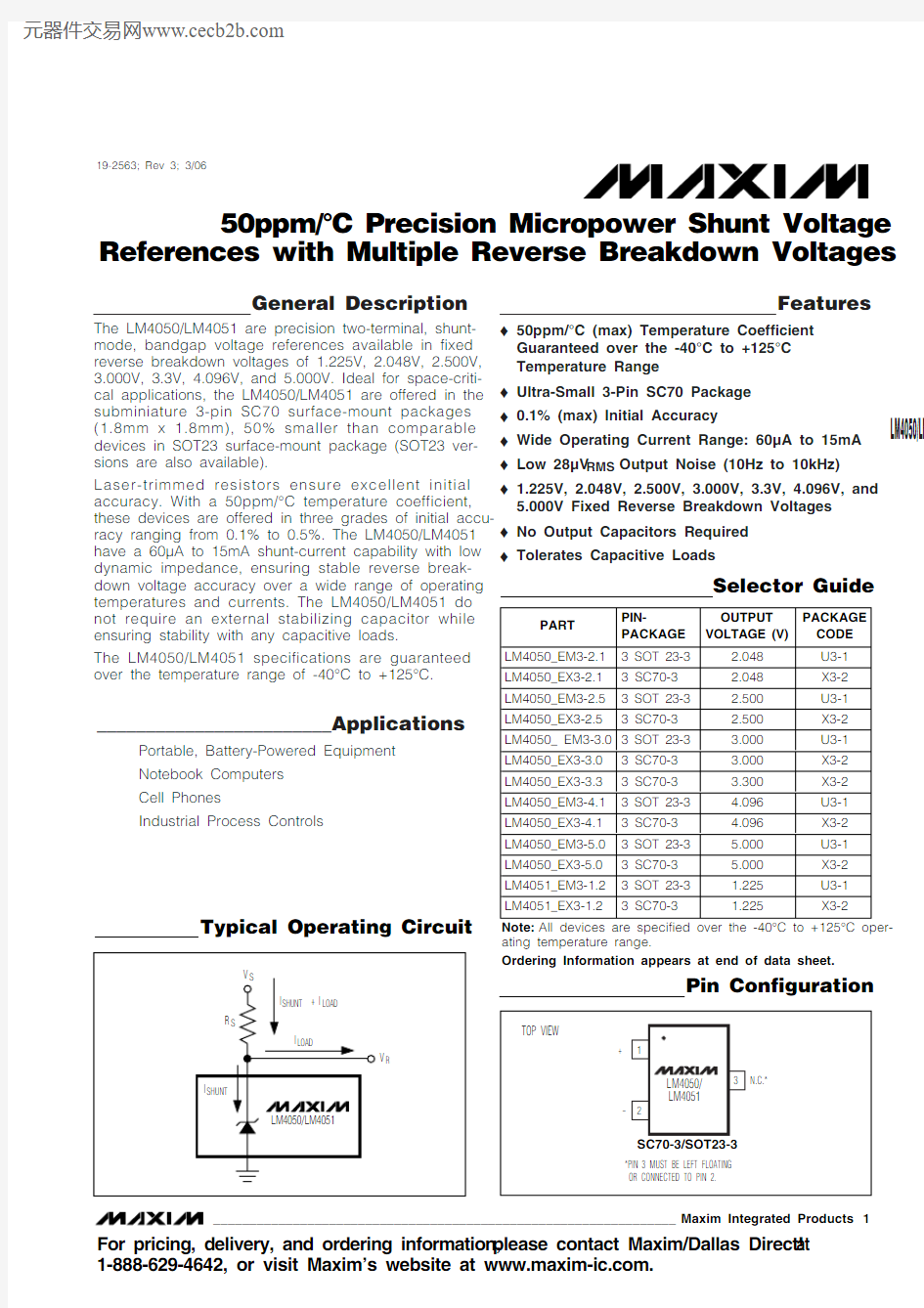
Typical Operating Circuit
Selector Guide
19-2563; Rev 3; 3/06
Ordering Information appears at end of data sheet.
For pricing, delivery, and ordering information,please contact Maxim/Dallas Direct!at 1-888-629-4642, or visit Maxim’s website at https://www.doczj.com/doc/424415017.html,.
L M 4050/L M 4051
50ppm/°C Precision Micropower Shunt Voltage
References with Multiple Reverse Breakdown Voltages
2_______________________________________________________________________________________
ABSOLUTE MAXIMUM RATINGS
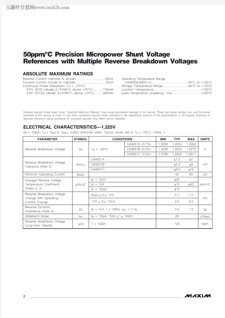
ELECTRICAL CHARACTERISTICS—1.225V
Stresses beyond those listed under “Absolute Maximum Ratings” may cause permanent damage to the device. These are stress ratings only, and functional operation of the device at these or any other conditions beyond those indicated in the operational sections of the specifications is not implied. Exposure to absolute maximum rating conditions for extended periods may affect device reliability.
Reverse Current (cathode to anode)..................................20mA Forward Current (anode to cathode)..................................10mA Continuous Power Dissipation (T A = +70°C)
3-Pin SC70 (derate 2.17mW/°C above +70°C)............174mW 3-Pin SOT23 (derate 4.01mW/°C above +70°C)..........320mW
Operating Temperature Range
LM4050/LM4051_E_ _ _................................-40°C to +125°C Storage Temperature Range.............................-65°C to +150°C Junction Temperature......................................................+150°C Lead Temperature (soldering, 10s)..................................+300°C
LM4050/LM4051
50ppm/°C Precision Micropower Shunt Voltage
References with Multiple Reverse Breakdown Voltages
_______________________________________________________________________________________3
ELECTRICAL CHARACTERISTICS—2.048V
L M 4050/L M 4051
50ppm/°C Precision Micropower Shunt Voltage
References with Multiple Reverse Breakdown Voltages
4_______________________________________________________________________________________
ELECTRICAL CHARACTERISTICS—2.500V
LM4050/LM4051
50ppm/°C Precision Micropower Shunt Voltage
References with Multiple Reverse Breakdown Voltages
ELECTRICAL CHARACTERISTICS—3.000V
L M 4050/L M 4051
50ppm/°C Precision Micropower Shunt Voltage
References with Multiple Reverse Breakdown Voltages
6_______________________________________________________________________________________
ELECTRICAL CHARACTERISTICS—4.096V
LM4050/LM4051
50ppm/°C Precision Micropower Shunt Voltage
References with Multiple Reverse Breakdown Voltages
_______________________________________________________________________________________7
RTOL R R where ?V R / ?T is the V R temperature coefficient, max ?T is the difference from the +25°C reference point to T MIN or T MAX ,and V R is the reverse breakdown voltage.
The total tolerance over the full temperature range for the different grades where max ?T = +100°C is shown below:?A grade: ±0.6% = ±0.1% ±50ppm/°C ?100°C ?B grade: ±0.7% = ±0.2% ±50ppm/°C ?100°C ?C grade: ±1.0% = ±0.5% ±50ppm/°C ?100°C
Note 3:Guaranteed by design.
ELECTRICAL CHARACTERISTICS—5.000V
L M 4050/L M 4051
50ppm/°C Precision Micropower Shunt Voltage
References with Multiple Reverse Breakdown Voltages
8_______________________________________________________________________________________
OUTPUT VOLTAGE vs. TEMPERATURE
(V OUT = 2.500V)
M A X 4050 t o c 02
TEMPERATURE (°C)
O U T P U T V O L T A G E (V )
110
85
60
35
10
-15
2.492
2.494
2.496
2.498
2.490
-40
135
OUTPUT VOLTAGE vs. TEMPERATURE
(V OUT = 5.000V)
M A X 4050 t o c 03
TEMPERATURE (°C)
O U T P U T V O L T A G E (V )
110
85
-15
10
35
60
4.989
4.9914.9934.9954.9974.999
5.0015.0034.987
-40
135
Typical Operating Characteristics
(I R = 100μA, SC70-3 package, T A = +25°C, unless otherwise noted.)
01234560
50
100
REVERSE CHARACTERISTICS AND MINIMUM OPERATING CURRENT
REVERSE CURRENT (μA)
R E V E R S E V O L T A G E (V )
LM4050-5.0V
REVERSE VOLTAGE vs. I SHUNT
I SHUNT (mA)
R E V E R S E V O L T A G E C H A N G E (m V )
15105
1
2345600
20
LM4050-2.5V
REVERSE VOLTAGE vs. I SHUNT
I SHUNT (mA)
R E V E R S E V O L T A G E C H A N G E (m V )
15
105
1
2
3
4
5
00
20
LM4050/LM4051
50ppm/°C Precision Micropower Shunt Voltage
References with Multiple Reverse Breakdown Voltages
_______________________________________________________________________________________
9
V G E N
V R A C -C O U P L E D
+25μA
-25μA
10mV/div
LM4050-5.0V
LOAD-TRANSIENT RESPONSE
40μs/div
I SHUNT = 100μA ± 25μA R L = 100k ?, SEE FIGURE 1.
V G E N
V R A C -C O U P L E D
+250μA
-250μA
10mV/div
LM4050-2.5V
LOAD-TRANSIENT RESPONSE
10μs/div
I SHUNT = 1mA ± 250μA R L = 10k ?, SEE FIGURE 1.
Typical Operating Characteristics (continued)
(I R = 100μA, SC70-3 package, T A = +25°C, unless otherwise noted.)
V G E N
V R A C -C O U P L E D
+25μA
-25μA
2mV/div
LM4050-2.5V
LOAD-TRANSIENT RESPONSE
LM4050 toc06
10μs/div
CH1: V GEN 2V/div
CH2: V R AC-COUPLED 2mV/div
I SHUNT = 100μA ± 25μA, R L = 100k ?, SEE FIGURE 1.
V G E N
V R A C -C O U P L E D
+2.5mA
-2.5mA
20mV/div LM4050-2.5V
LOAD-TRANSIENT RESPONSE
10μs/div
I SHUNT = 10mA ± 2.5mA R L = 1k ?, SEE FIGURE 1.
V G E N
V R A C -C O U P L E D
+2.5mA
-2.5mA
20mV/div
LM4050-5.0V
LOAD-TRANSIENT RESPONSE
10μs/div
I SHUNT = 10mA ± 2.5mA R L = 1k ?, SEE FIGURE 1.
V G E N
V R A C -C O U P L E D
+250μA
-250μA
10mV/div LM4050-5.0V
LOAD-TRANSIENT RESPONSE
10μs/div
I SHUNT = 1mA ± 250μA R L = 10k ?, SEE FIGURE 1.
Figure 1. Load-Transient Test Circuit
L M 4050/L M 4051
50ppm/°C Precision Micropower Shunt Voltage
References with Multiple Reverse Breakdown Voltages
10
______________________________________________________________________________________
V I N
V O U T
LM4050-5.0V
STARTUP CHARACTERISTICS
405020301060708090
RESPONSE TIME (μs)
5V 0
4V 2V SEE FIGURE 2.
0.1k
10k 1k
100k
1M
LM4050-2.5V
OUTPUT IMPEDANCE vs. FREQUENCY
FREQUENCY (Hz)
I M P E D A N C E (?)
1000
0.11
10
100Typical Operating Characteristics (continued)
(I R = 100μA, SC70-3 package, T A = +25°C, unless otherwise noted.)
V I N
V O U T
LM4050-2.5V
STARTUP CHARACTERISTICS
16208
124
24283236RESPONSE TIME (μs)
5V 0
2V 1V R S = 30k ?SEE FIGURE 2.
1
10010
1k
10k
LM4050-2.5V NOISE vs. FREQUENCY
L M 4050 t o c 16
FREQUENCY (Hz)
10,0001001000
N O I S E (n V /H z )
1
10010
1k
10k
LM4050-5.0V NOISE vs. FREQUENCY
L M 4050 t o c 17
FREQUENCY (Hz)
10,000
100
1000
N O I S E (n V /H z
)
0.1k
10k 1k
100k
1M
LM4050-5.0V
OUTPUT IMPEDANCE vs. FREQUENCY
FREQUENCY (Hz)
I M P E D A N C E (?)
100
0.1
110
Figure 2. Startup Characteristics Test Circuit
LM4050/LM4051
50ppm/°C Precision Micropower Shunt Voltage
References with Multiple Reverse Breakdown Voltages
______________________________________________________________________________________11
Applications Information
The LM4050/LM4051s’ internal pass transistors are used to maintain a constant output voltage (V SHUNT ) by sinking the necessary amount of current across a source resistor.The source resistance (R S ) is determined from the load current (I LOAD ) range, supply voltage (V S ) variations,V SHUNT , and desired quiescent current.
Choose the value of R S when V S is at a minimum and I LOAD is at a maximum. Maintain a minimum I SHUNT of 60μA at all times. The R S value should be large enough to keep I SHUNT less than 15mA for proper regulation when V S is maximum and I LOAD is at a minimum. To prevent damage to the device, I SHUNT should never exceed 20mA.
Therefore, the value of R S is bounded by the following equation:
[V S(MIN)- V R ] / [60μA + I LOAD(MAX)] > R S > [V S(MAX)- V R ] / [20mA + I LOAD(MIN)]
Choosing a larger resistance minimizes the total power dis-sipation in the circuit by reducing the shunt current (P D(TOTAL)= V S ?I SHUNT ). Provide a safety margin to incorporate the worst-case tolerance of the resistor used.Ensure that the resistor’s power rating is adequate, using the following general power equation:
PD R = I SHUNT ?(V S(MAX)- V SHUNT )
Output Capacitance
The LM4050/LM4051 do not require external capacitors for frequency stability and are stable for any output capacitance.
Temperature Performance
The LM4050/LM4051 typically exhibit output voltage temperature coefficients within ±15ppm/°C. The polari-ty of the temperature coefficients may be different from one device to another; some may have positive coeffi-cients, and others may have negative coefficients.
High Temperature Operation
The maximum junction temperature of the LM4050/LM4051 is +150°C. The maximum operating temperature for the LM4050/LM4051_E_ is +125°C. At a maximum load current of 15mA and a maximum output voltage of 5V, the parts dissipate 75mW of power. The power dissi-pation limits of the 3-pin SC70 call for a derating value of 2.17mW/°C above +70°C and thus for 75mW of power dissipation, the parts self-heat to 35.56°C above ambient temperature. If the ambient temperature is +125°C, the parts operate at 159.56°C, thereby exceeding the maxi-mum junction temperature value of +150°C. For high-temperature operation, care must be taken to ensure the combination of ambient temperature, output power dissi-pation, and package thermal resistance does not con-spire to raise the device temperature beyond that listed in the Absolute Maximum Ratings . Either reduce the out-put load current or the ambient temperature to keep the part within the limits.
Figure 3. Typical Operating Circuit
Chip Information
TRANSISTOR COUNT: 60PROCESS: BiCMOS
L M 4050/L M 4051
50ppm/°C Precision Micropower Shunt Voltage
References with Multiple Reverse Breakdown Voltages
12______________________________________________________________________________________
Ordering Information
LM4050/LM4051
50ppm/°C Precision Micropower Shunt Voltage
References with Multiple Reverse Breakdown Voltages
______________________________________________________________________________________
13
Package Information
(The package drawing(s) in this data sheet may not reflect the most current specifications. For the latest package outline information,go to https://www.doczj.com/doc/424415017.html,/packages .)
L M 4050/L M 4051
50ppm/°C Precision Micropower Shunt Voltage
References with Multiple Reverse Breakdown Voltages
Maxim cannot assume responsibility f or use of any circuitry other than circuitry entirely embodied in a Maxim product. No circuit patent licenses are implied. Maxim reserves the right to change the circuitry and specifications without notice at any time.
14____________________Maxim Integrated Products, 120 San Gabriel Drive, Sunnyvale, CA 94086 408-737-7600?2006 Maxim Integrated Products
Printed USA
is a registered trademark of Maxim Integrated Products, Inc.
Package Information (continued)
(The package drawing(s) in this data sheet may not reflect the most current specifications. For the latest package outline information,go to https://www.doczj.com/doc/424415017.html,/packages .)