R ecent years have witnessed an
increasing interest in direct
digital synthesis (DDS). The
technique emerged in the early 80s and
was probably known in principle for sev-
eral years before that. In those early
days, the highest output frequency at-
tainable was no more than a few MHz,
limited by the performance of the then
available logic ICs and digital-to-ana-logue converters (DACs).
With the advancement in semicon-ductor technology, the attainable per-formance has increased by leaps and bounds. DDS chips realised in gallium arsenide now provide output frequen-cies of over 400 MHz. Silicon technol-ogy delivers output frequencies in ex-cess of 300 MHz. However, when oper-ating at the top of the frequency range,the worst case levels of spurious out-puts have not changed much, still being in the region of 40 to 45 dB down on the wanted output.RF carrier generation The long-term frequency stability of an LC oscillator is generally poor. It is dif-ficult to construct a small inductor with stability much better than 0.01 per cent.Its spectral purity can only be increased by increasing the operating Q of the tuned circuit, which again is not easy,especially in the case of miniaturised rect synthesiser, since the output fre-quency is ultimately obtained from mas-ter crystal oscillator and has almost the purity of the master. The mix\filter\divide block provides 100kHz steps. Using the output as the input to another, similar block provides an out-put with 10kHz steps. Further blocks can be added to provide any required degree of resolution. High-performance filters and careful screening within and between blocks enable all non-harmonic spurious to be held at 80 dB down on the wanted output, at a price. The term ‘di-
rect analogue synthesiser’ is sometimes
used to distinguish it from the direct
digital synthesiser.
Direct synthesis is an attractive route in applications where high purity,low spurious outputs, and fast switch-ing are required, especially in lab and ATE equipment. But the size and cost make it difficult to apply in portable military or OEM equipment.Phase lock loop
The PLL (phase lock loop) technique is
widely applied in space applications
such as synchronising a receiver to a spacecraft signal with a doppler shift.
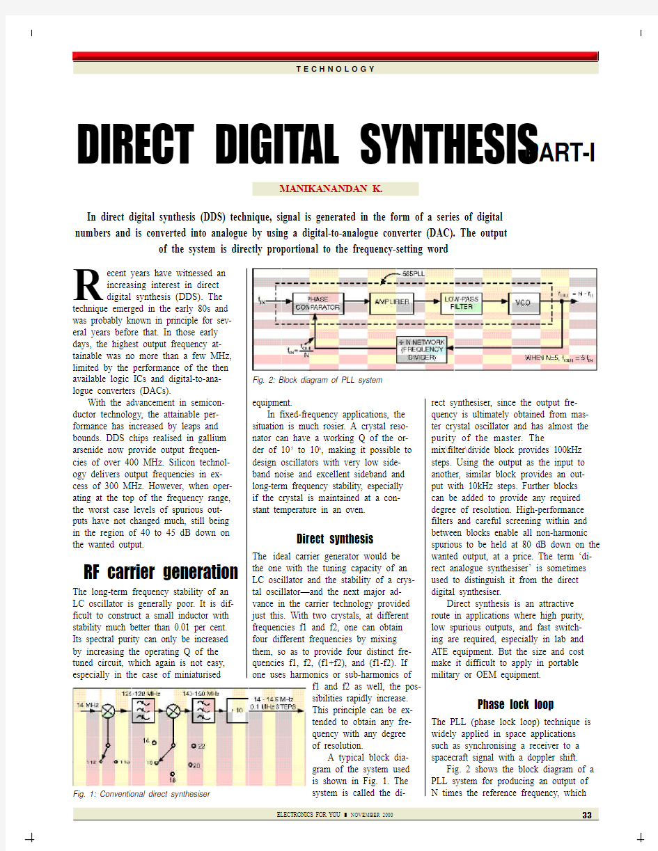
Fig. 2 shows the block diagram of a
PLL system for producing an output of
N times the reference frequency, which
Fig. 1: Conventional direct synthesiser
DIRECT DIGITAL SYNTHESIS
PART-I
MANIKANANDAN K.
In direct digital synthesis (DDS) technique, signal is generated in the form of a series of digital
numbers and is converted into analogue by using a digital-to-analogue converter (DAC). The output
of the system is directly proportional to the frequency-setting word
Fig. 2: Block diagram of PLL system
equipment.In fixed-frequency applications, the situation is much rosier. A crystal reso-nator can have a working Q of the or-der of 105 to 106, making it possible to design oscillators with very low side-band noise and excellent sideband and long-term frequency stability, especially if the crystal is maintained at a con-stant temperature in an oven.Direct synthesis The ideal carrier generator would be the one with the tuning capacity of an LC oscillator and the stability of a crys-tal oscillator—and the next major ad-vance in the carrier technology provided just this. With two crystals, at different frequencies f1 and f2, one can obtain four different frequencies by mixing them, so as to provide four distinct fre-quencies f1, f2, (f1+f2), and (f1-f2). If one uses harmonics or sub-harmonics of
f1 and f2 as well, the pos-
sibilities rapidly increase.This principle can be ex-
tended to obtain any fre-
quency with any degree
of resolution.
A typical block dia-gram of the system used
is shown in Fig. 1. The
system is called the di-
may itself be
obtained from
a crystal oscil-
lator. When
the loop is in
lock, the out-
put of the ‘di-
vide by N’
stage is at ex-
actly the same
frequency as the reference, but there will be a small phase offset, leading or lagging, result-ing in a DC component in the output of the mixer. This output is applied via a low-pass filter to a voltage-controlled os-cillator and results in exactly the de-sired output frequency.
If N is set to a different value, the output frequency will change; if N is changed to N+2, the output frequency will increase by twice the reference fre-quency. Here the step size is equal to the reference frequency. Enhancements of this technique, such as dual-modulus prescalars and multiple-loop architec-ture, enable fine frequency-resolution to be obtained comparatively at low cost.
A ‘fractional N’ approach enables the performance-to-price ratio to be im-proved even further, making the PLL synthesiser currently the most com-monly encountered scheme. PLL synthesisers offer fine frequency-reso-lution and very low levels of spurious outputs at comparatively low cost, but
cannot achieve the very same low lev-
els of close in phase noise as the direct
synthesiser. These have slow switching
times, due to loop-filter settling time.
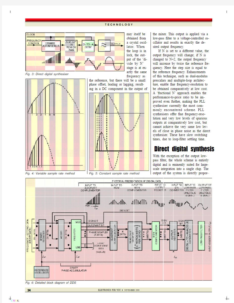
Direct digital synthesis
With the exception of the output low-
pass filter, the whole scheme is entirely
digital and is eminently suited for large-
scale integration into a single chip. The
output of the system is directly propor-
Fig. 6: Detailed block diagram of DDS
Fig. 4: Variable sample rate method
Fig. 5: Constant sample rate method
Fig. 3: Direct digital synthesiser
ELECTRONICS FOR YOU NOVEMBER 2000
34
tional to the frequency-setting word.In this technique, a signal is gener-ated in the form of a series of digital numbers and is converted into analogue by using a DAC (Fig. 3). These num-bers are stored in a memory device known as the memory lookup table.One way of generating the output is to output some points for every cycle of the sinewave. In this case, tuning is ef-fected by changing the rate at which the data is output (refer Fig. 4). It is difficult to get fine frequency-resolution using this method. In the second case,the rate at which data is output is kept constant. The basic idea is to store N uniformly spaced samples in the memory. The lowest output frequency contains N distinct samples. Now if one outputs every other point stored in the ROM at the same rate, one gets an out-put with twice the original frequency.So, if every Kth sample is taken, a K
times faster waveform will be obtained.The frequency resolution is same as that of the lowest frequency. This method is illustrated in Fig. 5.A more detailed block diagram of the DDS is shown in Fig. 6. The fre-quency setting word is given to the adder of a phase accumulator through a binary register. The adder adds the digital sig-nals from the binary regis-ter to the value of the accu-mulator register and up-dates the accumulator reg-ister with the most recent sum. This register trans-fers the digital data from the output of the adder to its input at every clockpulse, so as to make the accumula-
tor overflow at regular intervals. The
accumulator now addresses the ROM
through a quadrant complimentor.
Since all the amplitude information
for a full 360° sinewave is contained in
90° of information, only 90° of memory
mapping is required. The quadrant
complimentor simply helps the accumu-
lator to clock in both the directions, thus
giving 180° of the wave. Now the sine
complimentor changes sign and the pro-
cess is repeated to get the full sinewave.
The phase accumulator
Fig. 7 shows how the phase accumulator
works. For simplicity, a 6-bit accumula-
tor with three most significant bits con-
trolling the read only memory with just
eight memory locations has been as-
sumed. The output of the three most sig-
nificant bits from the latch to the
ROM needs to represent one com-
plete cycle of the output waveform,
so the eight values in the ROM
need to represent the amplitude
of the sinewave at 45° intervals.
The higher the value of the fre-
quency setting word, the fewer
cycles will be needed to cycle
through the ROM once, and hence
the higher output frequency. The
lowest possible output frequency results when the frequency-setting
word is 000001. In this case, ev-
ery eighth clock pulse advances
the ROM address by one.
The lookup table Fig. 8 shows the rest of the rudimen-
tary system, ROM, DAC, and output fil-
Fig. 9: 8Hz and 4Hz outputs from DDS, with a 64Hz clock
Fig. 7: The working of phase accumulator Fig. 8: The rest of the rudimentary DDS
(a) FSW=001000
(b) FSW=000100
ELECTRONICS FOR YOU NOVEMBER 2000
36ter. The values stored in ROM range from 1 representing the negative peak of the sinewave, to 255 representing the positive peak and definite points on a sinewave in offset binary. The value 128corresponds to the mean level (0V) of the waveform.Operation Imagine a 6-bit latch clocked at 64 Hz and the accumulator loaded with 000001(Fig. 7). Whatever the current value held in the latch, the output of the adder will exceed by 1. So, in the next clock pulse,the new value will be loaded into the latch, and so on repeatedly. Starting from the stage where the latch content is all zero, the three ROM address lines will be zero. The ROM will output 10000000, causing the DAC output to be 1.28V, corresponding to the zero value of sinewave at 0°. The output of the LPF will indeed be 0V,due to the blocking capacitor between it and the opamp; the purpose of the lat-ter being to turn the DAC’s current output back into a volt-age.Eight clock cycles later, the accu-mulator contents will be 001000; Ro will now be 1 so that the ROM output is 11011010, corresponding to the binary offset representation of the value of a sinewave at +45°, and accordingly the DAC output will becomes 2.18V.After 64 clock cycles, the accumula-tor is full and the DAC has delivered a complete cycle of stepwise representa-tion of a sinewave. Thus the lowest non-zero output frequency is 1 Hz or gener-ally Fclk/2oN, where N is the number of the accumulator bits (Fig. 9). If the fre-quency setting word is set to 000010,the whole process will complete one out-put cycle in half the clock period. So,Fclk/2oN is also the smallest frequency increment available.Fig. 4 also shows the instantaneous departure of the stepwise output ap-proximation from a continuous sinewave.These phase perturbations occur at a rate equal to the clock frequency, which is well above the highest output fre-
quency, and so these can be suppressed
by LPF even if one has a perfect DAC
with infinite resolution. Amplitude trun-cation errors cause sinewave represen-tations to be imperfect, resulting in har-monics in the output; whether these ap-pear in the output depends on com-manded output frequency. Apart from this possible harmonic content, the out-
put of 6-bit DDS is perfect at frequency
setting of 1, 2, 4, and 8 Hz. At other
frequencies, the operation becomes a
little more complicated.There are many other mechanisms that produce unwanted, non-harmonic,
spurious outputs. When the demanded fre-
quency is so high that the ROM only out-
puts a subset of its contents on each cycle,
the waveform into the LPF can take vari-ous quite different forms from a sinewave.
Fig. 10 shows some shapes the waveform
can take at a good frequency where the ROM address is incrementing so as to out-
put just four equally spaced locations.
Fig. 10: Waveform at a good frequency To be continued...