
3-D Heterogeneous Sensor System on a Chip for Defense and Security Applications Shekhar Bhansali, University of South Florida; Glenn H. Chapman, Simon Fraser University, Canada; Eby Friedman, University of Rochester; Yehea Ismail, Northwestern University;
P R Mukund, Rochester Institute of Technology; Dennis Tebbe, Harris Corporation;
Vijay Jain, University of South Florida
Contact: Prof. Vijay K. Jain
University of South Florida
Tampa, Florida 33620, USA
Phone: (813) 974-4741
Email: jain@https://www.doczj.com/doc/411117172.html,
Abstract
This paper describes a new concept for ultra-small, ultra-compact, unattended multi-phenomenological sensor systems for rapid deployment, with integrated classification-and-decision-information extraction capability from a sensed environment. We discuss a unique approach, namely a 3-D Heterogeneous System on a Chip (HSoC) in order to achieve a minimum 10X reduction in weight, volume, and power and a 10X or greater increase in capability and reliability – over the alternative planar approaches. These gains will accrue from (a) the avoidance of long on-chip interconnects and chip-to-chip bonding wires, and (b) the cohabitation of sensors, preprocessing analog circuitry, digital logic and signal processing, and RF devices in the same compact volume. A specific scenario is discussed in detail wherein a set of four types of sensors, namely an array of acoustic and seismic sensors, an active pixel sensor array, and an uncooled IR imaging array are placed on a common sensor plane. The other planes include an analog plane consisting of transductors and A/D converters. The digital processing planes provide the necessary processing and intelligence capability. The remaining planes provide for wireless communications/networking capability. When appropriate, this processing and decision-making will be accomplished on a collaborative basis among the distributed sensor nodes through a wireless network.
1. INTRODUCTION
An ultra-small, ultra-compact, unattended
multi-phenomenological sensor system
providing an integrated classification-and-
decision-information extraction capability
from the sensed environment, is illustrated in
Fig. 1. These systems are critically important
for defense and security applications.
Fig. 1 Integrated sensing
and information extraction
system.
from other sensor nodes important features
Unattended/Unmanned Ground, Ocean, and Air Sensor Technologies413
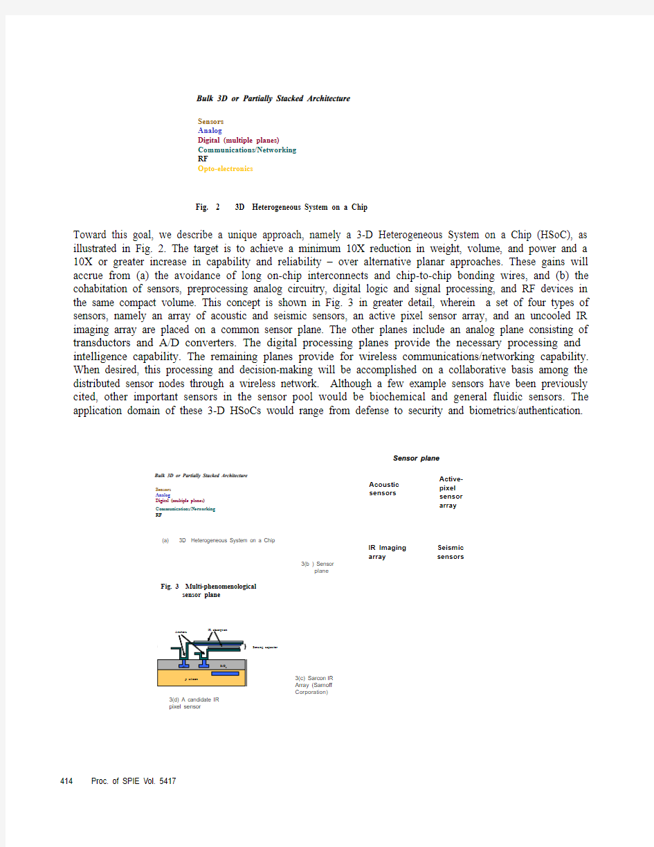
Toward this goal, we describe a unique approach, namely a 3-D Heterogeneous System on a Chip (HSoC), as illustrated in Fig. 2. The target is to achieve a minimum 10X reduction in weight, volume, and power and a 10X or greater increase in capability and reliability – over alternative planar approaches. These gains will accrue from (a) the avoidance of long on-chip interconnects and chip-to-chip bonding wires, and (b) the cohabitation of sensors, preprocessing analog circuitry, digital logic and signal processing, and RF devices in the same compact volume. This concept is shown in Fig. 3 in greater detail, wherein a set of four types of sensors, namely an array of acoustic and seismic sensors, an active pixel sensor array, and an uncooled IR imaging array are placed on a common sensor plane. The other planes include an analog plane consisting of transductors and A/D converters. The digital processing planes provide the necessary processing and intelligence capability. The remaining planes provide for wireless communications/networking capability. When desired, this processing and decision-making will be accomplished on a collaborative basis among the distributed sensor nodes through a wireless network. Although a few example sensors have been previously cited, other important sensors in the sensor pool would be biochemical and general fluidic sensors. The application domain of these 3-D HSoCs would range from defense to security and biometrics/authentication.
Sensors Fig. 2 3D Heterogeneous System on a Chip
Analog Digital (multiple planes)Communications/Networking RF Opto-electronics
3(c) Sarcon 3(d) A candidate IR
IR
Array (Sarnoff
Corporation)
pixel sensor
sensor plane
Sensors
Communications/Networking
Analog
Digital (multiple planes)
RF 414 Proc. of SPIE Vol. 5417
From a broader perspective, the realization of the concept will be ultra-small unattended 3-D multi-phenomenological sensor systems for rapid deployment with integrated classification-and-decision-information extraction capability from the sensed environment. Application scenarios of such 3-D Heterogeneous System on Chips
(HSoCs) are depicted in Figs. 4 and 5.
A conceptualization of one of many
applicable battlespace deployments is
illustrated in Fig. 4, and multi-level
networking of the HSoCs for a wide-
area coverage is shown in Fig. 5.
Fig. 4 A notional battlespace
Deployment of unattended 3-D
HSoC sensors (Harris Corp.)
Ad hoc wireless network of HSoC
multi-phenomenological sensors
Fig. 5 Multi-level networking of the HSoCs
Proc. of SPIE Vol. 5417 415
2. BREAKTHROUGH ADVANCES AND ENABLERS
This section consists of seven parts, Parts 2.1 to 2.7, as described below.
Breakthrough advances:
2.1 Integration of four diverse sensor types on a common silicon substrate
The first challenge is that of integrating acoustic and seismic sensors, an Active Pixel Sensor (APS) imager, and an IR bolometer on the same silicon substrate in ways that create reliable and high sensitivity devices. In addition, the following new challenges are envisioned: (a) combining the APS imager and IR bolometer into integrated hyperspectral pixels such that a single lens system can create multi-spectral images of a common imaged-volume ranging from visible (380-740 nm in three color ranges) to near-infrared (with an NIR APS to 1090 nm) to deep infrared spectra; and (b) exploring the possibility of a materials/fabrication process that would enable silicon itself to detect farther into the IR region with photocurrent type devices, thereby eliminating the need for micro-cantilever bolometer subpixels (see Fig. 6). Part b is highly speculative, albeit with a potential for significant pay-off, producing higher sensitivity and more tunable far IR detection. In addition to materials and fabrication process innovations, resolution of issues related to noise and defect tolerance as well as interfacing to the transduction plane, will be the pathway to successfully demonstrating this sensor plane.
Fig. 6 Combining
visible spectrum and
IR spectrum sensing into a single pixel
2.2 3-D heterogeneous system on a chip
Our 3-D System on a Chip (SoC) concept, illustrated in Figs. 2 and 3, will be developed with a view toward accurate detection of objects and events of interest with high sensitivity. The SoC includes a sensor plane which will be populated with a set of sensors, Sensor-1 …. Sensor-N, selected from a larger pool of sensors. In this paper we describe the use of acoustic sensors, active-pixel imaging array, IR imaging array, and seismic sensors. Also, it will be possible to soft-configure these sensors, remotely if desired, to suit a particular mission. For the accurate detection of objects and events of interest with high sensitivity, the multi-phenomenological data will be fused and processed in an integrative way . The feature extraction phase will utilize techniques such as ICA (Independent Component Analysis) upon the multi-domain data, in spectral and/or multi-resolution representations, which will be followed by either neural network techniques or Bayesian networks to arrive at classification-and-decision. Inter-plane switching will be used with a view toward fault tolerance, and dynamically allocating computational resources.
Besides the challenges of developing the individual planes with heterogeneous technologies, the following technology challenges are envisioned: (a) wafer thinning, (b) alignment and bonding, and (c) packaging, all in the context of 3D HSoC . Each of these four challenges will represent a significant leap forward with a large potential pay-off. In addition, the mapping of fusion algorithms, such as the ICA, integrally into a systolic DSP array on board the HSoC will represent a major advance.
(b) All silicon combined (a) Combined IR to visible pixel IR to visible pixel
416 Proc. of SPIE Vol. 5417
2.3 Modeling and design of 3-D HSoC at the physical and circuit levels
Some of the physical and circuit level issues that will be particularly important for HSoC 3-D circuits are thermal Issues, electromagnetic interference, interconnect design, and clock and power distribution. In 3-D technologies the device densities per unit volume are much larger (as compared to the planar counterparts) with some device layers buried between two other device layers with no easy way to radiate the generated heat, thereby resulting in higher temperatures. This kind of mutual dependence between the thermal and electrical characteristics of the circuit requires a simultaneous use of thermoelectrical modeling, simulation, and design methodologies. The electromagnetic interference in 3-D HSoCs structures will be different in nature from planar technologies in many respects. The existence of several layers of devices would make the problem of vertical coupling among devices directly through the intermediate substrates much harder. In addition, interconnect will run vertically over nontrivial distances across Si substrates, which are semiconducting, and produce coupling that is not present in planar technologies. Finally, the large variety of devices – analog, digital, and sensors – will pose a serious challenge in maintaining signal integrity.
This research will provide solutions to the aforementioned problems by also developing tools and design methodologies. Issues involved in 3-D HSoC design and possible design alternatives to handle these issues are illustrated in Fig. 7. The targeted verification platform for heterogeneous SoCs, including thermal effects, is shown in Fig. 8. This verification and analysis platform will be used iteratively throughout the design methodology to enhance the resulting circuit design to satisfy target performance and reliability metrics .
Fig. 7 Design methodology
Fig. 8 Modeling and verification for 3D HSoC platform
Enablers:
The following will serve as enablers for propelling and completing the development of the first concept prototype. It is important to note, however, that each of these enablers represents a major technological advance.
2.4 Advanced RF design and ad hoc networking
RF components -- active and passive circuits, MEMS, and planar antenna, will be integrated onto the 3-D structure. An external plane (see
Fig. 9) together with some of the adjacent planes will support embedded
RF cores, leading to ultra-high performance systems within a small volume. Another aspect of the concept objective is to develop a low cost yield-enhancing non-intrusive probing methodology for on-chip testing
of multi-GHz RF circuits, analog circuits, and mixed-signal circuits. The final result will be a fully integrated BIST architecture for the RF plane. Fig. 9 RF plane (an outer plane)
Process Noise and
Power Timing variations Frequency
response
interference Feedback 3-D interconnect
3-D clock and
Thermoelectrical electromagnetic functionality and power
design Synchronization Low power design power distribution analysis and design 3-D compatibility
Proc. of SPIE Vol. 5417 417
2.5 Hierarchical 3-D interconnection network
Critical to the design and performance of the 3-D HSoC will be the interconnection network, binding the diverse planes and elements. In order to facilitate on-chip communication while minimizing the number of vertical channels, we propose to use a hierarchical interconnection network, such as the TESH, “Tori connected mESHes (TESH).” The key features of the TESH network are its hierarchy, thus allowing exploitation of computation locality as well as easy expansion, and compatibility with 3-D VLSI implementation since far fewer vertical wires are required than almost all known multi-computer networks (see Fig. 10). Redundancy will be used to circumvent faulty devices, including failed sensors and defective interconnect, especially faulty vias for vertical interconnect. Extension of the network to mixed signals will be a key focus in that a single network will bind all devices and computing modules.
Fig. 10 Vertical links needed
for various interconnection
networks
2.6 Reconfigurable DSP cells and mapping of advanced fusion techniques such as ICA
The central idea for managing the design gap is platform-based design, in which predefined architectures support the rapid creation of application-specific derivatives. In line with this strategy, we will develop and use a Field Programmable Function Array (FPFA)-based design methodology for the digital planes of the 3-
D HSoC system. We have developed coarse grain cells designed for high functionality, performance, and
reconfigurability. It is proposed to further develop and use these cells for the 3-D SoC with signal and image processing applications, including the mapping of the ICA technique to demix and separate the independent signal components of the multi-phenomenological sensor data for subsequent detection of objects/events.
Another function of the DSP cell array will be to compensate for the actual positions of the functional sensors, which may be different from the nominal positions due to defect circumvention.
2.7 Micro-system integration, packaging, and multifunctional materials
Harris Corporation has developed technology and processes that enable the integration and packaging for 3-
D HSoC, including techniques that accommodate the environmental accesses that are required by the
multiple onboard sensors (acoustic, seismic, active-pixel sensor imaging array, and infrared imaging array).
Harris will facilitate the transition to 3-D-HSoC-required integration, packaging and testing technologies by applying its innovative micro-miniaturization techniques within this new domain. The use of multifunctional materials will enable the ongoing improvement of micro-miniaturization by merging the functions of
interconnection-substrates and packaging, and by eliminating most or all of the discrete passive components in the RF plane. In the framework of 3-D HSoC, the goal is volumetric efficiency, and Harris will contribute by utilizing its embedded passives, and conformal antenna technologies. Harris Corporation is focused on the system effectiveness of 3D-HSoC for defense-related capabilities, and accordingly will incorporate wireless 418 Proc. of SPIE Vol. 5417
ad hoc networking in the communication architecture. Figure 11 depicts an objective monolithic packaging concept. A stack of five planes is shown, but some of these in turn could be stacks themselves. Integrated into the sensor window in Fig. 11(b) is a conformal cross-bow antenna. Also note the test interface, which will be removed after the final test.
(a) (b) Fig. 11 Objective
monolithic package
3. DETAILS OF TECHNICAL APPROACH
The discussion is based in part on the different planes of the 3-D HSoC (see Fig. 2), and on the beakthrough advances and enabling technologies discussed in Section 2.
3.1 Sensor Plane:
All four types of sensors – seismic, acoustic, visible imaging (APS), and IR imaging – will be co-located on a common silicon substrate.
Acoustic and Seismic Sensors: Micromachined microphones will be used to detect acoustic and seismic waves on the order of 0.01Hz to 20 kHz. The source of perturbation will be spatially resolved based on the tailored design of an array of acoustic membranes. The required detection range will be met by arraying the basic microphone unit. Higher sensitivity and a flatter frequency response will be achieved by membranes of varying materials, thickness, and dimensions. To overcome possible fabrication or run time defects, a redundant array will be used; for example, if an N ×N functional array is targeted, an N ×(N+1) array will be fabricated and alternate routing used to harvest a working N ×N array. DSP algorithms, in the digital stack, will be designed to compensate for changes in sensor distribution created by this harvesting. The response of the microphone would be tuned, exploiting the geometry of the diaphragm. The process flows would be investigated to fabricate the membranes of varying thickness on the same silicon membrane. Fabrication of multi-material microphones would be carried out to investigate the frequency response, sensitivity, and directivity for improved performance of the sensor as compared to the use of a single material membrane array.
Visible and IR Imaging Sensors:
HyperSpectral Detectors combining Active Pixel Sensors (APS) and IR bolometers: RGB APS, IR filtered APS and long wavelength bolometers will all be integrated into each pixel for spectral identification of emissions/reflections in order to achieve superior object discrimination.
New APS Designs: High reliability redundant APS pixels, with immunity to both high levels of fabrication defects and field time defects (e.g., due to radiation), and with low area, will be developed. Enhanced Adaptive Range Multiexposure APS will provide both expanded dynamic range and pixel by pixel real time
Cable Connect
to Antenna Proc. of SPIE Vol. 5417 419
exposure adjustment. Image Time Differentiation APS would automatically detect the time related changes between two scenes, potentially providing both intensity and spectral time base changes within the APS.
Silicon Enhanced Long IR Detection: the potential for using heavy doping (with unconventional materials) to create silicon electronic detectors more sensitive to longer IR waves than those constrained by the current bandgap limit of 1.12 eV (corresponding to a maximum wavelength of 1071 nm) will be investigated.
Reduced bandgaps are envisioned ranging from 0.6 to 0.25 eV with corresponding wavelengths of 2000 nm to 5000 nm.
3.2 Analog Plane Innovations:
The analog plane would house transductors and A/D converters. Innovations would include the use of resource sharing. To reduce volume and conserve power, resource-sharing will be used as shown in Fig. 12.
Specifically, this economy will be realized by allowing multiple sensors to share transductors, and multiple transductors/AD-converters to share a common signal processing array. Another important aspect will be defect and fault tolerance through redundancy and reconfiguration.
Fig. 12 Economy and flexibility
through resource sharing
3.3 3-D Network Through All Planes:
In order to facilitate the on-chip communication, while minimizing the number of vertical channels, we propose to use the TESH (“T ori connected m ESH es”) hierarchical interconnection network. Extension of the network to mixed signals will be a key focus. Also, redundancy to overcome possible defects in the modules or interconnect will be employed. This redundancy will enable successful communication among the modules and devices despite fabrication and processing defects. The latter would include defects in via generation due to misalignment or inadequate aspect ratios.
3.4 Reconfigurable DSP Cells and Mapping of Advanced Fusion Through ICA:
A coarse grain reconfigurable cell approach will be developed and implemented for the digital planes
targeted at high functionality, performance, and reconfigurability of the 3-D HSoC signal and image processing objectives, including the mapping of the ICA technique to demix and separate the independent components of the multi-phenomenological sensor data for subsequent detection of objects/events.
Reconfigurability will be useful both for mapping multiple applications to the same cell array, as well as for defect tolerance. A novel single-cycle nonlinear processor cell will be used to achieve a 10X or greater reduction in nonlinear computations that are pervasive in ICA computations.
3.5 Development of 3-D HSoC Physical and Functional Integration Technology: The Heterogeneous System
on a Chip (SoC) concept will be developed with a view toward accurate detection of objects and events of interest with high sensitivity. Practical issues will include (a) placement of subsystems and subunits in the appropriate stack, more specifically one of its planes; selecting optimum areas and thicknesses of the various planes; contacts for vertical wires, (b) the thinning of the planes of the stack and their alignment and
bonding, (c) generation of the deep vias through multiple planes and stacks for vertical communication, (d)
420 Proc. of SPIE Vol. 5417
clock and power distribution, and (d) thermal management. At the functional end, the issues are (a) sensor signal conditioning in the analog plane/stack, including A/D conversion, (b) redundancy for overcoming defects, (c) resource-sharing to minimize volume, (d) inter-plane switching for reducing hot-spots and load-balancing, and (e) mapping of multiple DSP functions to a common pool of coarse-grain computational cells.
3.6 Clock and Power Distribution Networks for 3-D HSoC: A 3-D system will require effective strategies for synchronizing the data flow. Different synchronization strategies will target a 3-D topology. If fully synchronous, a novel clock distribution architecture will be required to manage the synchronization constraints for a 3-D system. These architectures and related circuit constraints will be integrated into a cohesive methodology for designing high performance 3-D oriented clock distribution networks. Architectures for power distribution that support a non-uniform HSoC structure will be developed to support these requirements. Additionally, DC and transient voltage drops within the power network will be incorporated into an overall methodology for designing a 3-D based power distribution network.
3.7 Interconnect Design: Issues such as locally distributed noise, power density issues, and asymmetric thermal characteristics such as local hot spots and related power removal constraints, all operating under high performance (high speed and low power) and density requirements, will be addressed and an effective solution produced.
3.8 Simultaneous Thermo-Electrical Analysis and Design of 3-D SoC Circuits: In 3-D technologies, device densities per unit volume are much larger with some device layers buried between two other device layers with no easy way to radiate the generated heat, resulting in higher temperatures. These high temperatures produce adverse effects on the device mobility and interconnect reliability. In addition, these thermal effects are in turn dependent on the electrical and run time characteristics of the circuit since the radiated heat depends on the switching activity and the circuit characteristics. This kind of mutual dependence between the thermal and electrical characteristics of the circuit will be addressed through simultaneous thermoelectrical modeling, simulation, and related design methodologies.
3.9 Electromagnetic Coupling in 3-D SoC Circuits: Electromagnetic interference in 3-D HSoCs structures is different in nature from planar digital technologies in many respects. The existence of several layers of devices will make vertical coupling between devices much more challenging. Previously, devices coupled through a single substrate. However, in a 3-D scenario, devices can couple directly through the intermediate substrates, significantly changing the nature of the problem. In addition, interconnect will run vertically over nontrivial distances across semiconducting silicon substrates, causing new forms of coupling effects that are not present in planar technologies. Finally, the large number of analog and digital circuits as well as sensors will pose a serious challenge for maintaining signal integrity. These problems will be addressed though new models and simulation techniques, and associated design techniques.
3.10 Micro-system Integration, Packaging, and Testing: In this technology transition to 3D heterogeneous sensor systems on a chip, the associated integration, packaging and testing technologies will also undergo a transition. Harris' innovative micro-miniaturization techniques will facilitate this transition when applied to the new tasks and challenges within the 3D HSoC context.
3.11 Multifunctional Materials and Embedded Passives: The use of multifunctional materials enables the ongoing improvement of micro-miniaturization by merging the functions of interconnection substrates and packaging and by eliminating most or all discrete passive components. Harris Corporation's embedded-passives and conformal-antenna technologies provide important contributions to the volumetric efficiency goal.
Proc. of SPIE Vol. 5417 421
4. GENERAL DISCUSSION OF OTHER RESEARCH IN THIS AREA
Three dimensional (3-D) integration, combining multiple layers of planar devices with a high density of in-plane and out-of-pane interconnects, is a promising approach to extending performance beyond device and interconnect scaling limits [1]-[14]. 3-D integration provides high device integration density, high interconnectivity, reduction of long global wires and the related power consumption, novel architectures, and improved performance for system-on-chip (SOC) applications. One of the primary benefits of 3D integration is the freedom and efficiency in partitioning and integrating modules with mixed-signal or mixed-technology designs, such as logic, memory, analog, RF/Microwave, FPGA and Optical I/O. As compared to conventional ICs, 3-D ICs can mitigate processing complexity and cost in the heterogeneous integration of disparate materials such as Si, SiGe, GaAs or different circuit technologies such as CMOS, BiCMOS, and optoelectronic devices on separate device layers. Furthermore, improved noise coupling isolation among logic and analog/RF circuit blocks on separate device layers can be achieved with judicious separation of device types and the reduction of noise coupling through a common substrate.
MIT Lincoln Labs have developed an example of a 3-D IC [1]-[3] for low power and high bandwidth using a bonding approach. They have integrated two layers, namely an SOI wafer with imaging circuits and inverters to an SOI wafer with A/D converter circuits and inverters, using a combination of deep and shallow vias.
This work shows the feasibility of stacking SOI circuits to build 3D ICs with dense vias and the results are being applied to the development of higher performance systems. A Cornell University team has developed
a new single crystal Si layering and front-end-compatible interconnect fabrication process [4], [5]
appropriate for mixed signal applications. Called MLBS, the technique combines a dual damascene process for in-plane and out-of-plane interconnects, chemical-mechanical polishing for bondable roughness, direct wafer bonding, and critical low–temperature silicon layering. A Japanese team from the Association of Super-Advanced Electronics Technologies has reported a 3-D stacking technology [6] using advanced bonding processes and DRIE for vias filled with copper to form microbump interconnections.
Indeed, the work of numerous other teams [7]-[13] has been examined. However, building ultra-small, ultra-compact, unattended multi-phenomenological sensor system, with integrated classification-and-decision-information extraction capability from the sensed environment on a 3-D Heterogeneous Sensor System Chip, has not been attempted, and is far and away more challenging. Our multi-university team together with our industry partner, Harris Corporation, will develop this capability, thereby achieving a quantum advance in technology, focusing on mission-specific performance.
5. MAJOR INNOVATIONS
As stated in the abstract, the goal of this endeavor is to build ultra-small, ultra-compact, unattended multi-phenomenological sensor systems for rapid deployment with integrated classification-and-decision-information extraction capability from the sensed environment. Toward this goal, we propose a unique approach, namely a 3-D Heterogeneous System on a Chip (HSoC), as illustrated previously in Figs. 2, 3, and
11. This section delineates the anticipated innovations. On one of the planes of the 3-D HSoC, four types of
sensors, namely an array of acoustic and seismic sensors, an active pixel sensor array, and an uncooled IR imaging array will be placed. Indeed, if successful, a plug-and-play capability can be imagined. That is, the sensor plane could, in the future, be populated with a set of N sensors, selected from a larger pool of sensors according to the requirements of the mission, and plugged into the 3-D HSoC without physically altering the other planes. Also, it would be possible to soft-configure these sensors, remotely if desired, to suit a particular mission. For the accurate detection of objects and events of interest with high sensitivity, the multi-phenomenological data will be fused and processed in an integrative way. The feature extraction phase will 422 Proc. of SPIE Vol. 5417
utilize techniques such as ICA upon the multi-domain data, in spectral and/or multi-resolution representations, which will be followed by either neural network techniques or Bayesian networks to arrive at the classification-and-decision. The major challenges will be in the integration of the various planes with heterogeneous technologies into the overall stack, and indeed also in forming the planes which might themselves be formed as a stack of homogeneous technology planes.
From a higher-level perspective, our vision encompasses no less than the beginning of the “3-D integrated-system” technology revolution that will eventually supersede the 2-D “integrated circuit” revolution. As stated in Subsection 2.5E, building ultra-small, ultra-compact, unattended multi-phenomenological sensor systems, with integrated classification-and-decision-information extraction capability from the sensed environment on a 3-D Heterogeneous Sensor System Chip, has not been attempted. The successful realization of this objective will benefit not only the nation’s defense, but will also provide the industry a launch pad for a new generation of innovation. A list of anticipated technical advances is given below.
o3-D Heterogeneous system on a chip
o Multiple functionalities on the same chip: sensing, processing, and networking
o Vertical integration of the planes
o Multiphenomenological sensors on a common plane and on the same silicon substrate
o Combined APS and IR imaging pixels leading to a merged hyperspectral APS and IR imaging array o Multi-exposure APS
o Novel reconfigurable DSP array, and sensor fusion at multiple stages
o Hierarchical interconnection network with aggregation for vertical links
o Collaborative sensing
o Efficient methodology for designing 3-D systems
o Simulation, prediction, and minimization of heating effects
o Power minimized architectures, placement, and technologies
o Drastic reduction in interconnect lengths and the efficient use of repeaters
o Design tools for 3-D systems
o RF plane subsystem
o Stand alone packaging of HSoC
o Defect and fault tolerance at all planes of the 3-D HSoC
Reduction in size and weight: since an integrated system with the capability of four types of sensors, namely arrays of acoustic and seismic sensors, an active pixel sensor array, and an IR imaging array, together with classification-and-decision-information extraction capability from the sensed environment does not, to our knowledge, exist, it is not possible to correctly estimate the size in terms of today’s planar technology. Even so, we estimate the size with today’s planar technology to be at least 6”×6”×1”. Correspondingly, a very approximate sizing of the HSoC, excluding the package, is shown in Fig. 13.
approximately
HSoC: four types of sensors (acoustic, seismic, visible spectrum and IR imaging),
decision capability, and ad hoc networking. Not shown is the package.
Fig. 13 Reduction in volume
Proc. of SPIE Vol. 5417 423
Figure of Merit: A figure-of-merit is the following:
where ‘accuracy ’ is the accuracy or reliability from a functional or detection point of view. A 100X or greater increase in FoM relative to current implementations is envisioned. Naturally, the ‘accuracy’ will consider the probability of missing a true event of interest and the probability of a false alarm.
5. CONCLUSIONS
A 3-D Heterogeneous System on a Chip (HSoC) concept for ultra-small, ultra-compact, unattended multi-phenomenological sensor systems for rapid deployment, with integrated classification-and-decision-information extraction capability from the sensed environment was presented in this paper. This approach is aimed at a minimum 10X reduction in weight, volume, and power, and a 10X or greater increase in capability and reliability – over the alternative planar approaches. Remote unattended sensors are invaluable for defense and security if they are deployable, affordable, sensitive, specific, reliable, long-lived, and rapidly transmit usable information to where it is needed. The 3-D HSoC technology is a way to provide improvements in sensory data collection, in conjunction with improved detection, classification and autonomous decision-making, in a smaller, lighter, package with greater energy efficiency and effective wireless inter-networking. This is all the more important because the 3-D HSoC technology is also a high risk but possible next step in the continuing integrated circuit revolution.
REFERENCES
[1] J. Burns, L. McIlrath, C. Keast, C. Lewis, A. Loomis, K. Warner and P. Wyatt, “Three-dimensional integrated circuits for low-power, high-bandwidth systems on a chip,” Proc. IEEE International Solid-State Circuits Conference , pp. 268-269, Feb. 2001.
[2] J. Burns, L. McIlrath, L. Hopwood, C. Keast, D. P. Vu, K. Warner, P. Wyatt , “An SOI-based three-dimensional integrated circuit technology,” Proc. IEEE International SOI Conference , pp. 20 -21, Oct. 2000
[3] L. McIlrath, “A low-power low-noise ultrawide-dynamic-range CMOS imager with pixel-parallel A/D conversion,” IEEE Journal of Solid-State Circuits , pp. 846 -853, May 2001
[4] X. Lei, C.C. Liu, H.-S. Kim, S.K. Kim and S. Tiwari, “Three-dimensional integration: technology, use, and issues for mixed-signal applications,” IEEE Trans. on Electron Devices , pp. 601-609, March 2003.
[5] S. Tiwari, H.-S. Kim, S. Kim, A. Kumar, C.C. Liu and L . Xue, “Three-dimensional integration in silicon electronics,” Proc. IEEE Lester Eastman Conference on High Performance Devices , pp. 24-33, Aug. 2002.
[6] Y. Tomita, T. Morifuji, T. Ando, M. Tago, R. Kajiwara, Y. Nemoto, T. Fujii , Y. Kitayama and K. Takahashi , “Advanced packaging technologies on 3D stacked LSI utilizing the micro interconnections and the layered microthin encapsulation,” Proc. Electronic Components and Technology Conference , pp. 353-360, May - June 2001
[7] M. Chan , “The potential and realization of multi-layers three-dimensional integrated circuit,” Proc. 6th International Conference on Solid-State and Integrated-Circuit Technology, pp. 40-45, Oct. 2001.
[8] S. J. Abou-Samra, P. A. Aisa, A. Guyot and B. Courtois, “3D CMOS SOI for high performance computing,” Proc. International Symposium on Low Power Electronics and Design , pp. 54-58, Aug. 1998.
[9] V. W. C. Chan, P. C. H. Chan and M. Chan, “3D integrated circuit using large grain polysilicon film,” Proc. 6th International Conference on Solid-State and Integrated-Circuit Technology , pp.58-61, Oct. 2001.
[10] Y. Hayashi, S. Wada, K. Kajiyana, K. Oyama, R. Koh, S. Takahashi and T. Kunio , “Fabrication of three-dimensional IC using cumulatively bonded IC (CUBIC) technology,” Proc. Symposium on VLSI Technology , pp. 95-96, June 1990.
[11] A. Kamazaki, Y. Itoh, A. Wada, K. Morimoto and Y. Tomita, “4-lyaer 3-D IC technologies for parallel signal processing,” Proc. International Electronic Devices Meeting , pp. 599-602, June 1991.
[12] K. Kioi, T. Shinozaki, S. Toyoyoma, K. Shirakawa, K. Ohtake and S. Tsuchimoto, “Design and implementation of a 3D-LSI
image sensing processor,” IEEE Journal of Solid State Circuits , pp. 1130 – 1139, Aug. 1992.
[13] K. C. Saraswat, S. J. Souri, V. Subramaniam, A.R. Joshi and A.W. Wang, “Novel 3D Structures [ICs],” Proc. IEEE International SOI Conference , pp. 54-55, Oct. 1999.
Power Accuracy Volume Weight FoM ×?},{424 Proc. of SPIE Vol. 5417
照度计算公式 E=(Φ×n×N×MF×UF)/A 式中,E=工作面的维护平均照度(lx); Φ=灯初始光通量(lm) n= 每个灯具所含光源的数量 N=灯具数量 MF=设备维护系数 UF=设备利用系数 A=工作面的面积 一个灯具在给室内的利用系数UF是照射到工作面上所有光通量与设备中所有灯发出的光通量之比。这一系数包括反射光、相互反射光及来自灯具的直接光。它的值取决于房间的形状、高度、墙壁的反射率及灯具的光强分布。 MF=设备维护系数一般取之间。 UF=设备利用系数(由于范围更宽)一般取之间。 一般室内取,体育取 维护系数:一般取~ 实例:一个100平方米的办公室,层高3米,工程方要求的照度是
500lx,要用我公司的3*36W T8灯盘,请问要用多少套用上面的公司计算,取MF(设备维护系数)为,UF(设备利用系数)为,假设要用3*36W T8灯盘X套, 公式E=(Φ×n×N×MF×UF)/A 即:500=(3300×3×X××)/100 X= 约9套 照度计算方法 利用系数法计算平均照度 平均照度 (Eav) = 光源总光通量(N*Ф)*利用系数(CU)*维护系数(MF) / 区域面积(m2) (适用于室内或体育场的照明计算) 利用系数: 一般室内取,体育取 维护系数:一般取~ 举例 1:室内照明: 4×5米房间,使用3×36W隔栅灯9套 平均照度=光源总光通量×CU×MF/面积 =(2500×3×9)××÷4÷5 =1080 Lux 结论:平均照度1000Lux以上 举例 2: 体育馆照明:20×40米场地, 使用POWRSPOT 1000W金卤灯60套 平均照度=光源总光通量×CU×MF/面积
小学数学课程标准 第一部分前言 数学是研究数量关系和空间形式的科学。数学与人类发展和社会进步息息相关,随着现代信息技术的飞速发展,数学更加广泛应用于社会生产和日常生活的各个方面。数学作为对于客观现象抽象概括而逐渐形成的科学语言与工具,不仅是自然科学和技术科学的基础,而且在人文科学与社会科学中发挥着越来越大的作用。特别是20世纪中叶以来,数学与计算机技术的结合在许多方面直接为社会创造价值,推动着社会生产力的发展。 数学是人类文化的重要组成部分,数学素养是现代社会每一个公民应该具备的基本素养。作为促进学生全面发展教育的重要组成部分,数学教育既要使学生掌握现代生活和学习中所需要的数学知识与技能,更要发挥数学在培养人的理性思维和创新能力方面的不可替代的作用。 一、课程性质 义务教育阶段的数学课程是培养公民素质的基础课程,具有基础性、普及性和发展性。数学课程能使学生掌握必备的基础知识和基本技能;培养学生的抽象思维和推理能力;培养学生的创新意识和实践能力;促进学生在情感、态度与价值观等方面的发展。义务教育的数学课程能为学生未来生活、工作和学习奠定重要的基础。 二、课程基本理念 1.数学课程应致力于实现义务教育阶段的培养目标,要面向全体学生,适应学生个性发展的需要,使得:人人都能获得良好的数学教育,不同的人在数学上得到不同的发展。 2.课程内容要反映社会的需要、数学的特点,要符合学生的认知规律。它不仅包括数学的结果,也包括数学结果的形成过程和蕴涵的数学思想方法。课程内容的选择要贴近学生的实际,有利于学生体验与理解、思考与探索。课程内容的组织要重视过程,处理好过程与结果的关系;要重视直观,处理好直观与抽象的关系;要重视直接经验,处理好直接经验与间接经验的关系。课程内容的呈现应注意层次性和多样性。 3.教学活动是师生积极参与、交往互动、共同发展的过程。有效的教学活动是学生学与教师教的统一,学生是学习的主体,教师是学习的组织者、引导者与合作者。 数学教学活动应激发学生兴趣,调动学生积极性,引发学生的数学思考,鼓励学生的创造性思维;要注重培养学生良好的数学学习习惯,使学生掌握恰当的数学学习方法。 学生学习应当是一个生动活泼的、主动的和富有个性的过程。除接受学习外,动手实践、自主探索与合作交流同样是学习数学的重要方式。学生应当有足够的时间和空间经历观察、实验、猜测、计算、推理、验证等活动过程。 教师教学应该以学生的认知发展水平和已有的经验为基础,面向全体学生,注重启发式和因材施教。教师要发挥主导作用,处理好讲授与学生自主学习的关系,引导学生独立思考、主动探索、合作交流,使学生理解和掌握基本的数学知识与技能、数学思想和方法,获得基本的数学活动经验。 4.学习评价的主要目的是为了全面了解学生数学学习的过程和结果,激励学生学习和改进教师教学。应建立目标多元、方法多样的评价体系。评价既要关注学生学习的结果,也要重视学习的过程;既要关注学生数学学习的水平,也要重视学生在数学活动中所表现出来的情感与态度,帮助学生认识自我、建立信心。 5.信息技术的发展对数学教育的价值、目标、内容以及教学方式产生了很大的影响。数学课程的设计与实施应根据实际情况合理地运用现代信息技术,要注意信息技术与课程内容的整合,注重实效。要充分考虑信息技术对数学学习内容和方式的影响,开发并向学生提供丰富的学习资源,把现代信息技术作为学生学习数学和解决问题的有力工具,有效地改进教与学的方式,使学生乐意并有可能投入到现实的、探索性的数学活动中去。 三、课程设计思路 义务教育阶段数学课程的设计,充分考虑本阶段学生数学学习的特点,符合学生的认知规律和心理特征,有利于激发学生的学习兴趣,引发数学思考;充分考虑数学本身的特点,体现数学的实质;在呈现作为知识与技能的数学结果的同时,重视学生已有的经验,使学生体验从实际背景中抽象出数学问题、构建数学模型、寻求结果、解决问题的过程。 按以上思路具体设计如下。
一、关于led灯具SSL规范的概述 今年 5 月份,LED 灯具的能源之星的规范,美洲已公开草案;估计今年的 8 至9 月份,会上升为最终版本,并于9 个月后,即08 年6 月份,授理ENERGY STAR申请;本规范是由 美国能源部DOE 负责组织, Lighting Research Center 技术负责; 二、重要流行词 1、SSL (Solid-State Lighting 固态照明) vs. Semi-conductor Lighting (半导体照明) vs. LED Lighting (LED 照明) SSL:(在Internet 网络上,SSL 在90 年代即有, 是Internet 传输加密协议缩略词SSL =Secure Socket Layer; )如今,在国外,有关研究 LED 的政府机构,公司和机构,很流行用 SSL 代替LED; 然而,目前,SSL 还没有给出正式定义,在美国的LRC 网站上,“What is SSL?”,只是解释为: SSL 是区别于传统的灯丝白帜发光和气体放电发光原理,由半导体的电子发光,包括LED,OLED,Laser Diode (LD),light-emitting polymers. 2、半导体照明 (Semi-conductor Lighting), 在中国政府机构,沿用过去的称谓“半导体照明”较多;但是,LED 产品,技术和标准,美国领先其他国家许多;中国也会随美国技术潮流使用SSL 称谓,尤其在DOE 公开本规范后; 三、我们的目的 1、本规范是第一部LED 照明的性能参数标准,指明了LED 照明的基本要求; 2、LED 灯具的ENERGY STAR认证,要在08 年6 月前讨论;但是,我们可以提前借鉴此规范化的参数标准,应用到研发品质行销工作中,是有帮助的; 3、本规范是如何基于荧光灯,建立 SSL-LED 灯具的光效目标和特性参数要求:
先计算色坐标。方法是,必须先有光谱P(λ)。 然后光谱P(λ),与三刺激函数X(λ)、Y(λ)、Z(λ),分别对应波长相乘后累加,得出三刺激值,X、Y、Z。 那么色坐标x=X/(X+Y+Z)、Y/(X+Y+Z) 一般,光谱是从380nm到780nm,间隔5nm,共81个数据。 X(λ)、Y(λ)、Z(λ),是CIE规定的函数,对应光谱,各81个数据,色度学书上可以查到。 再计算色温,例如色度坐标x=0.5655,y=0.4339。 用“黑体轨迹等温线的色品坐标”有麦勒德、色温、黑体轨迹上的(xyuv)、黑体轨迹外的(xyuv)。我们用xy的数据来举例。 一、为了方便表达,把黑体轨迹上的x写成XS、y写成YS,黑体轨迹外的x写成XW、y写成YW。 先把每一行斜率K算出,K=(YS-YW)/(XS-XW),写在表边上。 例如: 麦勒德530斜率K1=(.4109-.3874)/(.5391-.5207)=1.3352 麦勒德540斜率K2=(.4099-.3866)/(.5431-.5245)=1.2527 麦勒德550斜率K3=(.4089-.3856)/(.5470-.5282)=1.2394 二、找出要计算的x=.5655、y=.4339这个点,在哪两条等温线之间,就是这点到两条等温线距离一正一负。 如果不知道它的大概色温,计算就繁了;因为你说是钠灯,那么它色温在1800到1900K之间。 用下公式算出这点到麦勒德530,1887K等温线的距离D1 D1=((x-YS)-K(y-XS))/((1+K×K)开方) =((.4339-.4109)-1.3352(.5655-.5391))/((1+1.3352×1.3352)开方) =(.023-.03525)/(1.6682)=-.0073432 再计算出这点到麦勒德540,1852K等温线的距离D2 D2=((.4339-.4099)-1.2527(.5655-.5431))/((1+1.2527×1.2527)开方) =(.024-.02806)/(1.6029)=-.0025329 因为D1、D2都是负数,没找到。 再计算出这点到麦勒德550,1818K等温线的距离D3 D3=((.4339-.4089)-1.2394(.5655-.5470))/((1+1.2394×1.2394)开方) =(.025-.02293)/(1.6029)=+.0013005 D2负、D3正,找到了。D2对540麦勒德记为M2、D3对550麦勒德记为M3 三、先把距离取绝对值。按比例得出这点麦勒德M,公式是
小学数学新课标解读 《全日制义务教育数学课程标准(修定稿)》(以下简称《标准》)是针对我国义务教育阶段的数学教育制定的。根据《义务教育法》.《基础教育课程改革纲要(试行)》的要求,《标准》以全面推进素质教育,培养学生的创新精神和实践能力为宗旨,明确数学课程的性质和地位,阐述数学课程的基本理念和设计思路,提出数学课程目标与内容标准,并对课程实施(教学.评价.教材编写)提出建议。 《标准》提出的数学课程理念和目标对义务教育阶段的数学课程与教学具有指导作用,教学内容的选择和教学活动的组织应当遵循这些基本理念和目标。《标准》规定的课程目标和内容标准是义务教育阶段的每一个学生应当达到的基本要求。《标准》是教材编写.教学.评估.和考试命题的依据。在实施过程中,应当遵照《标准》的要求,充分考虑学生发展和在学习过程中表现出的个性差异,因材施教。为使教师更好地理解和把握有关的目标和内容,以利于教学活动的设计和组织,《标准》提供了一些有针对性的案例,供教师在实施过程中参考。 二、设计理念 数学是研究数量关系和空间形式的科学。数学与人类的活动息息相关,特别是随着计算机技术的飞速发展,数学更加广泛应用于社会生产和日常生活的各个方面。数学作为对客观现象抽象概括而逐渐形成的科学语言与工具,不仅是自然科学和技术科学的基础,而且在社会科学与人文科学中发挥着越来越大的作用。数学是人类文化的重要组成部分,数学素养是现代社会每一个公民所必备的基本素养。数学教育作
为促进学生全面发展教育的重要组成部分,一方面要使学生掌握现代生活和学习中所需要的数学知识与技能,一方面要充分发挥数学在培养人的科学推理和创新思维方面的功能。 义务教育阶段的数学课程具有公共基础的地位,要着眼于学生的整体素质的提高,促进学生全面.持续.和谐发展。课程设计要满足学生未来生活.工作和学习的需要,使学生掌握必需的数学基础知识和基本技能,发展学生抽象思维和推理能力,培养应用意识和创新意识,在情感.态度与价值观等方面都要得到发展;要符合数学科学本身的特点.体现数学科学的精神实质;要符合学生的认知规律和心理特征.有利于激发学生的学习兴趣;要在呈现作为知识与技能的数学结果的同时,重视学生已有的经验,让学生体验从实际背景中抽象出数学问题.构建数学模型.得到结果.解决问题的过程。为此,制定了《标准》的基本理念与设计思路。 基本理念 数学课程应致力于实现义务教育阶段的培养目标,体现基础性.普及性和发展性。义务教育阶段的数学课程要面向全体学生,适应学生个性发展的需要,使得:人人都能获得良好的数学教育,不同的人在数学上得到不同的发展。课程内容既要反映社会的需要.数学学科的特征,也要符合学生的认知规律。它不仅包括数学的结论,也应包括数学结论的形成过程和数学思想方法。课程内容要贴近学生的生活,有利于学生经验.思考与探索。内容的组织要处理好过程与结果的关系,直观与抽象的关系,生活化.情境化与知识系统性的关系。课程内容
色温对照表 - 以K为单位的光色度对照表 色温指的是光波在不同的能量下,人类眼睛所感受的颜色变化。 在色温的计算上,是以 Kelvin 为单位,黑体幅射的0° Kelvin= 摄氏 -273 ° C 做为计算的起点。将黑体加热,随着能量的提高,便会进入可见光的领域,例如,在2800 ° K 时,发出的色光和灯泡相同,我们便说灯泡的色温是2800 ° K。 可见光领域的色温变化,由低色温至高色温是由橙红 --> 白 --> 蓝。 色温的特性 1. 在高纬度的地区,色温较高,所见到的颜色偏蓝。 2. 在低纬度的地区,色温较低,所见到的颜色偏红。 ( <---- 低色温 ------------------ 高色温 ----> ) 3. 在一天之中,色温亦有变化,当太阳光斜射时,能量被( 云层、空气 )吸收较多,所以色温较低。当太阳光直射时,能量被吸收较少,所以色温较高。 4.Windows 的 sRGB 色彩模型是以6500 ° K 做为标准色温,以 D65 表示之。 5. 清晨的色温大约在4400 ° K。 6. 高山上色温大约在6000 ° K。 色温对照表 - 以K为单位的光色度对照表 烛焰 1500 家用白灯 2500-3000 60瓦的充气钨丝灯 2800 100瓦的钨丝灯 2950 1000瓦的钨丝灯 3000 500瓦的投影灯 2865 500瓦钨丝灯 3175 3200K的泛光灯 3200 琥珀闪光信号灯 3200 R32反射镜泛光灯 3200 锆制的浓弧光灯 3200 1,2,4号泛光灯,反射镜泛光灯 3400 暖色的白荧光灯 3500 切碎箔片,清晰闪光灯信号 3800 冷色的白荧光灯 4500 白昼的泛光灯 4800 白焰碳弧灯 5000 M2B闪光信号灯 5100 正午的日光 5400 高强度的太阳弧光灯 5550 夏季的直射太阳光 5800 早上10点到下午3点的直射太阳光 6000 蓝闪光信号灯 6000 白昼的荧光灯 6500 正午晴空的太阳光 6500 阴天的光线 6800-7000 高速电子闪光管 7000 来自灰蒙天空的光线 7500-8400
小学数学课程标准 一、总目标 通过义务教育阶段的数学学习,学生能: 1. 获得适应社会生活和进一步发展所必需的数学的基础知识、基本技能、基本思想、基本活动经验。 2. 体会数学知识之间、数学与其他学科之间、数学与生活之间的联系,运用数学的思维方式进行思考,增强发现和提出问题的能力、分析和解决问题的能力。 3. 了解数学的价值,提高学习数学的兴趣,增强学好数学的信心,养成良好的学习习惯,具有初步的创新意识和实事求是的科学态度。 总目标从以下四个方面具体阐述: 知识技能 1.经历数与代数的抽象、运算与建模等过程,掌握数与代数的基础知识和基本技能。 2.经历图形的抽象、分类、性质探讨、运动、位置确定等过程,掌握图形与几何的基础知识和基本技能。 3.经历在实际问题中收集和处理数据、利用数据分析问题、获取信息的过程,掌握统计与概率的基础知识和基本技能。 4.参与综合实践活动,积累综合运用数学知识、技能和方法等解决简单问题的数学活动经验。 数学思考
1.建立数感、符号意识和空间观念,初步形成几何直观和运算能力,发展形象思维与抽象思维。 2.体会统计方法的意义,发展数据分析观念,感受随机现象。 3.在参与观察、实验、猜想、证明、综合实践等数学活动中,发展合情推理和演绎推理能力,清晰地表达自己的想法。 4.学会独立思考,体会数学的基本思想和思维方式。 问题解决 1.初步学会从数学的角度发现问题和提出问题,综合运用数学知识解决简单的实际问题,增强应用意识,提高实践能力。 2.获得分析问题和解决问题的一些基本方法,体验解决问题方法的多样性,发展创新意识。 3.学会与他人合作交流。 4.初步形成评价与反思的意识。 情感态度 1.积极参与数学活动,对数学有好奇心和求知欲。 2.在数学学习过程中,体验获得成功的乐趣,锻炼克服困难的意志,建立自信心。 3.体会数学的特点,了解数学的价值。 4.养成认真勤奋、独立思考、合作交流、反思质疑等学习习惯,形成实事求是的科学态度。 总目标的这四个方面,不是相互独立和割裂的,而是一个密切联系、相互交融的有机整体。在课程设计和教学活动组织中,应同时兼顾这四
利用系数法计算平均照度 平均照度(Eav) = 光源总光通量(N*Ф)*利用系数(CU)*维护系数(MF) / 区域面积(m2) (适用于室内或体育场的照明计算) 利用系数:一般室内取0.4,体育取0.3 维护系数:一般取0.7~0.8 举例 1:室内照明: 4×5米房间,使用3×36W隔栅灯9套 平均照度=光源总光通量×CU×MF/面积 =(2500×3×9)×0.4×0.8÷4÷5 =1080 Lux 结论:平均照度1000Lux以上 举例 2:体育馆照明:20×40米场地,使用POWRSPOT 1000W金卤灯 60套 平均照度=光源总光通量×CU×MF/面积 =(105000×60)×0.3×0.8÷20÷40 =1890 Lux 结论:平均水平照度1500Lux以上 某办公室平均照度设计案例:
设计条件:办公室长18.2米,宽10.8米,顶棚高2.8米,桌面高0.85米,利用系数0.7,维护系数0.8,灯具数量33套,求办公室内平均照度是多少? 灯具解决方案:灯具采用DiNiT 2X55W 防眩日光灯具,光通量3000Lm,色温3000K,显色性Ra90以上。 根据公式可求得: Eav = (33套X 6000Lm X 0.7 X 0.8) ÷ (18.2米X 10.8米) = 110880.00 ÷ 196.56 m2 = 564.10Lux 备注: 照明设计必须必须要求准确的利用系数,否则会有很大的偏差,影响利用系数的大小,主要有以下几个因素: *灯具的配光曲线 *灯具的光输出比例 *室内的反射率,如天花板、墙壁、工作桌面等 *室内指数大小 复杂的区域照明设计,需利用专业的照明设计软件,进行电脑模拟计算。 浅析照度计算的研究与探讨 照度计算是实现建筑光环境设计总体构想的重要手段。采用单位容量法计算,能较好平衡准确度与简便度,为照度计算的实际运用加大了可操作性。
小学数学新课程标准(修改稿)解读 一、前言 《全日制义务教育数学课程标准(修改稿)》(以下简称《标准》)是针对我国义务教育阶段的数学教育制定的。根据《义务教育法》、《基础教育课程改革纲要(试行)》的要求,《标准》以全面推进素质教育,培养学生的创新精神和实践能力为宗旨,明确数学课程的性质和地位,阐述数学课程的基本理念和设计思路,提出数学课程目标与内容标准,并对课程实施(教学、评价、教材编写)提出建议。 《标准》提出的数学课程理念和目标对义务教育阶段的数学课程与教学具有指导作用,教学内容的选择和教学活动的组织应当遵循这些基本理念和目标。《标准》规定的课程目标和内容标准是义务教育阶段的每一个学生应当达到的基本要求。《标准》是教材编写、教学、评估、和考试命题的依据。在实施过程中,应当遵照《标准》的要求,充分考虑学生发展和在学习过程中表现出的个性差异,因材施教。为使教师更好地理解和把握有关的目标和内容,以利于教学活动的设计和组织,《标准》提供了一些有针对性的案例,供教师在实施过程中参考。 二、设计理念 数学是研究数量关系和空间形式的科学。数学与人类的活动息息相关,特别是随着计算机技术的飞速发展,数学更加广泛应用于社会生产和日常生活的各个方面。数学作为对客观现象抽象概括而逐渐形成的科学语言与工具,不仅是自然科学和技术科学的基础,而且在社会科学与人文科学中发挥着越来越大的作用。数学是人类文化的重要组成部分,数学素养是现代社会每一个公民所必备的基本素养。数学教育作为促进学生全面发展教育的重要组成部分,一方面要使学生掌握现代生活和学习中所需要的数学知识与技能,一方面要充分发挥数学在培养人的科学推理和创新思维方面的功能 义务教育阶段的数学课程具有公共基础的地位,要着眼于学生的整体素质的提高,促进学生全面、持续、和谐发展。课程设计要满足学生未来生活、工作和学习的需要,使学生掌握必需的数学基础知识和基本技能,发展学生抽象思维和推理能力,培养应用意识和创新意识,在情感、态度与价值观等方面都要得到发展;要符合数学科学本身的特点、体现数学科学的精神实质;要符合学生的认知规律和心理特征、有利于激发学生的学习兴趣;要在呈现作为知识与技能的数学结果的同时,重视学生已有的经验,让学生体验从实际背景中抽象出数学问题、构建数学模型、得到结果、解决问题的过程。为此,制定了《标准》的基本理念与设计思路基本理念。 (一)总:六大理念 1、人人学有价值的数学,人人都能获得必需的数学,不同的人在数学上得到不同的发展 2、数学是人们生活、劳动和学习必不可少的工具,数学是一切重大技术发展的基础,数学是一种文化。 3、数学学习的内容要有利于学生主动地进行观察、实验、猜测、验证、推理、与交流,动手实践、自主探索与合作交流是学生学习数学的重要方式。 4、学生是数学学习的主人,教师是数学学习的组织者、引导者、合作者。 5、评价的目的—了解学生的数学学习历程,改进教师的教学;目标多元,方法多样;重过程,轻结果;关注情感态度。 6、把现代信息技术作为学生学习数学和解决问题的强有力的工具。 (二)分六大理念的解读: 数学课程应致力于实现义务教育阶段的培养目标,体现基础性、普及性和发展性。义务教育阶段的数学课程要面向全体学生,适应学生个性发展的需要,使得:人人都能获得良好的数学教育,不同的人在数学上得到不同的发展。 1、关于数学课程的功能 (1)“人人学有价值的数学”是指作为教育内容的数学,应当是适合学生在有限的学习时间里接触、了解和掌握的数学。 怎样理解有价值的数学?
首先,你要有一“黑体轨迹等温线的色品坐标”表。此表“色度学”书中有。 然后,运用内插法和三角形垂足法计算色温 在“黑体轨迹等温线的色品坐标”表中,每一行(每一色温)有“黑体轨迹上”x、y,设为x1、y1,“黑体轨迹外” x、y,设为x2、y2。用仪器测得色度坐标x、y设为x0、y0。 从最低色温起,取其x1、y1,x2、y2;代入D1 = (x0-x1)(y1-y2)-(x1-x2)(y0-y1),如果D1 = 0则(相关)色温得到。如果D1不等于0,取上一行x1、y1,x2、y2;代入D2 = (x0-x1)(y1-y2)-(x1-x2)(y0-y1),如果D2 = 0则(相关)色温得到。如果D2不等于0,判断D1*D2是否小于0。 如果D1*D2大于0,使D1 = D2,再取上一行x1、y1,x2、y2;代入D2 = (x0-x1)(y1-y2)-(x1-x2)(y0-y1),如果D2 = 0则(相关)色温得到。如果D2不等于0,判断D1*D2是否小于0。 如果D1*D2小于0,则找到“测得坐标在这两条等温线之间”。D1、D2取绝对值,相对应色温为T1、T2。 那么CCT ≈ T1 + D1 * (T1+T2) / (D1+D2) 如果一直找不到D1*D2小于0,那是测得坐标在∞(无穷大)等温线左下方,那片区域是没有(相关)色温的。 按理说,离开黑体轨迹一定距离,就没有(相关)色温概念了,可是现在给搞混淆了。
或者,你在附图中,把你坐标点上去,看左右两条等温线的色温,估算出。 特征点对应的色坐标值和色温 光源点X坐标Y坐标色温(K) A 0.4476 0.4074 2854 B 0.3484 0.3516 4800 C 0.3101 0.3162 6800 D 0.313 0.329 6500 E 0.3333 0.3333 5500
计算公式: 灯具数量=(平均照度E×面积S)/(单个灯具光通量Φ×利用系数CU ×维护系数K ) 室内灯具平均照度计算公式 平均照度(Eav)= 单个灯具光通量Φ×灯具数量(N)×空间利用系数(CU)×维护系数(K)÷地板面积(长×宽) 因为误差总是存在:20%-30%,所以建议使用专业的照明设计软件进行精确计算,而对于特殊或场地条件所限,而不能采用照明软件模拟计算时,在计算地板、桌面、作业台面平均照度可以用下列基本公式进行,略估算出灯具照度(勒克斯lx)=光通量(流明lm)/面积(平方米m^2) 即平均1勒克斯(lx)的照度,是1流明(lm)的光通量照射在1平方米(m^2)面积上的亮度。 公式说明: 1、单个灯具光通量Φ,指的是这个灯具内所含光源的裸光源总光通量值。 2、空间利用系数(CU),是指从照明灯具放射出来的光束有百分之多少到达地板和作业台面,所以与照明灯具的设计、安装高度、房间的大小和反射率的不同相关,照明率也随之变化。 常用灯盘在3米左右高的空间使用,其利用系数CU可取0.6--0.75之间; 悬挂灯铝罩,空间高度6--10米时,其利用系数CU取值范围在0.7--0.45; 筒灯类灯具在3米左右空间使用,其利用系数CU可取0.4--0.55; 光带支架类的灯具在4米左右的空间使用时,其利用系数CU可取0.3--0.5。 3、维护系数(K),是指伴随着照明灯具的老化,灯具光的输出能力降低和光源的使用时间的增加,光源发生光衰或由于房间灰尘的积累,致使空间反射效率降低,致使照度降低而乘上的系数。 一般较清洁的场所,如客厅、卧室、办公室、教室、阅读室、医院、高级品牌专卖店、艺术馆、博物馆等维护系数K取0.8; 一般性的商店、超市、营业厅、影剧院、加工车间、车站等场所维护系数K取0.7; 而污染指数较大的场所维护系数K则可取到0.6左右。 (光源光通量)(CU)(MF) /照射区域面积 适用于室内,体育照明,利用系数(CU):一般室内取0.4,体育取0.3 1. 灯具的照度分布 2. 灯具效率 3. 灯具在照射区域的相对位置 4. 被包围区域中的反射光 维护系数MF=(LLD)X(LDD)一般取0.7~0.8 举例:1、室内照明,4×5米房间,使用3×36W隔栅灯9套 计算公式: 平均照度=光源总光通×CU×MF/面积
解读《义务教育小学数学课程标准》(2011年版)一 【新旧课标比较】与旧课标相比,新课标从基本理念、课程目标、内容标准 到实施建议都更加准确、规范、明了和全面。具体变化如下: 一、总体框架结构的变化 2001年版分四个部分:前言、课程目标、内容标准和课程实施建议。 2011年版把其中的“内容标准”改为“课程内容”。前言部分由原来的基本理念和设计思路,改为课程基本性质、课程基本理念和课程设计思路三部分。 二、关于数学观的变化 2001年版: 数学是人们对客观世界定性把握和定量刻画、逐渐抽象概括、形成方法和理论,并进行广泛应用的过程。 数学作为一种普遍适用的技术,有助于人们收集、整理、描述信息,建立数学模型,进而解决问题,直接为社会创造价值。 2011年版: 数学是研究数量关系和空间形式的科学。 数学作为对于客观现象抽象概括而逐渐形成的科学语言与工具。 数学是人类文化的重要组成部分,数学素养是现代社会每一个公民应该具备的基本素养。 三、基本理念“三句”变“两句”,“6条”改“5条” 2001年版“三句话”: 人人学有价值的数学,人人都能获得必需的数学,不同的人在数学上得到不同的发展。 2011年版“两句话”: 人人都能获得良好的数学教育,不同的人在数学上得到不同的发展。 “6条”改“5条”: 在结构上由原来的6条改为5条,将2001年版的第2条关于对数学的认识整合到理念之前的文字之中,新增了对课程内容的认识,此外,将“数学教学”与“数学学习”合并为数学“教学活动”。 2001年版:数学课程——数学——数学学习——数学教学活动——评价——现代信息技术 2011年版:数学课程——课程内容——教学活动——学习评价——信息技术 四、理念中新增加了一些提法 要处理好四个关系 数学课程基本理念(两句话) 数学教学活动的本质要求 培养良好的数学学习习惯 注重启发式 正确看待教师的主导作用 处理好评价中的关系
A不同时刻直射光的色温值:直射日光 色温值(K) 中午日光5500 日出后二小时4400 日落前二小时4300 日出后一个半小时4000 日出后40 分钟2900 日出后30分钟2400 日落前30分钟2300 日出后20分钟2100 日出.日落时1900 B不同季节和天气情况下自然光的色温值: 自然光的变化3-5月 6 -8月9-10月11-12月直射日光9-15时5800 5800 5550 5500 直射9时前15时后5400 5600 5000 4900 日光+天空光9-15时6500 6500 6200 6200 日光+天空光9前15后6100 6200 5900 5700 日光+天空光5900 5800 5900 5700 阴天6700 6950 6750 6500
蓝色天空27000 14000 12000 12000 C常见人工光源的色温值: 光源种类 色温值 电子闪光灯光5300-6000 1000-5000W卤素灯5000-6000 高色温碳弧灯5500 白色碳弧灯5000 500W高色温摄影灯3200 500W摄影泛光灯3400 摄影卤素灯光3000-4000 1300W新闻碘钨灯3200 200W普通灯炮2980 100W普通灯泡2900 75W普通灯泡2800 40W普通灯泡2650 蜡烛光1850 色温究竞是指什么? 我们知道,通常人眼所见到的光线,是由光的三原色(红绿蓝)组成的7种色光的光谱所组成。色温就是专门用来量度光线的颜色成分的。
用以计算光线颜色成分的方法,是19世纪末由英国物理学家洛德·凯尔文所创立的,他制定出了一整套色温计算法,而其具体界定的标准是基于以一黑体辐射器所发出来的波长。 凯尔文认为,假定某一纯黑物体,能够将落在其上的所有热量吸收,而没有损失,同时又能够将热量生成的能量全部以“光”的形式释放出来的话,它便会因受到热力的高低而变成不同的颜色。例如,当黑体受到的热力相当于500—550℃时,就会变成暗红色,达到1050一1150℃时,就变成黄色……因而,光源的颜色成分是与该黑体所受的热力温度相对应的。只不过色温是用凯尔文(°K、也就是绝对温度)的色温单位来表示,而不是用摄氏温度(℃)单位表示的。在加热铁块的过程中,黑色的铁在炉温中逐渐变成红色,这便是黑体理论的最好例子。当黑体受到的热力使它能够放出光谱中的全部可见光波时,它就由红转变橙黄色、黄色最后变成白色,通常我们所用灯泡内的钨丝就接近于这个黑体。色温计算法就是根据以上原理,用°K来表示受热钨丝所放射出光线的色温。根据这一原理,任何光线的色温是相当于上述黑体散发出同样颜色时所受到的“温度”。 颜色实际上是一种心理物理上的作用。所有颜色印象的产
人教版小学数学四年级下册新课标解读 崔庙镇实验小学 四年级
人教版小学数学四年级下册新课标解读 一、教材的主要内容: 小数的意义与性质,小数的加法和减法,四则运算,运算定律与简便计算,三角形,位置与方向,折线统计图,数学广角和数学综合运用活动等。 其中小数的意义与性质,小数的加法和减法,运算定律与简便计算,以及三角形是本册的重点教学内容。 二、教材的学习目标 1、理解小数的意义和性质,体会小数在日常生活中的应用,进一步发展数感,掌握小数点位置移动引起小数大小变化的规律,掌握小数的加法和减法。 2、掌握四则混合运算的顺序,会进行简单的整数四则混合运算;探索和理解加法和乘法的运算定律,会应用它们进行一些简便运算,进一步提高计算能力。 3、认识三角形的特性,会根据三角形的边、角特点给三角形分类,知道三角形任意两边之和大于第三边以及三角形的内角和是 180°。 4、初步掌握确定物体位置的方法,能根据方向和距离确定物体的位置,能描述简单的路线图。 5、认识折线统计图,了解折线统计图的特点,初步学会根据统计图和数据进行数据变化趋势的分析,进一步体会统计在现实生活中的作用。
6、经历从实际生活中发现问题、提出问题、解决问题的过程,体会数学在日常生活中的作用,初步形成综合运用数学知识解决问题的能力。 7、了解解决植树问题的思想方法,培养从生活中发现数学问题的意识,初步培养探索解决问题有效方法的能力,初步形成观察、分析及推理的能力。 8、体会学习数学的乐趣,提高学习数学的兴趣,建立学好数学的信心。 9、养成认真作业、书写整洁的良好习惯。 三、教材的编写特点: 本册实验教材具有内容丰富、关注学生的经验与体验、体现知识的形成过程、鼓励算法多样化、改变学生的学习方式,体现开放性的教学方法等特点。同时,本实验教材还具有下面几个明显的特点。 1. 改进四则运算的编排,降低学习的难度,促进学生的思维水平的提高。 四则运算的知识和技能是小学生学习数学需要掌握的基础知识和基本技能。以往的小学数学教材在四年级时要对以前学习过的四则运算知识进行较为系统的概括和总结,如概括出四则运算的意义和运算定律等。对于这些相关的内容,本套实验教材在本册安排了“四则运算”和“运算定律与简便计算”两个单元。“四则运算”单元的教学内容主要包括四则混合运算和四则运算的顺序。而关于四则运算的意义没有进行概括,简化了教学内容,降低了学习的难度。
什么是色温 色温的定义色温指的是光波在不同的能量下,人类眼睛所感受的颜色变化。在色温的计算上,是以Kelvin 为单位,黑体幅射的0°Kelvin= 摄氏-273 ° C 做为计算的起点。将黑体加热,随着能量的提高,便会进入可见光的领域,例如,在2800 °K 时,发出的色光和灯泡相同,我们便说灯泡的色温是2800 °K。可见光领域的色温变化,由低色温至高色温是由橙红--> 白--> 蓝。色温的特性 1. 在高纬度的地区,色温较高,所见到的颜色偏蓝。 2. 在低纬度的地区,色温较低,所见到的颜色偏红。( <---- 低色温------------------ 高色温----> ) 3. 在一天之中,色温亦有变化,当太阳光斜射时,能量被( 云层、空气)吸收较多,所以色温较低。当太阳光直射时,能量被吸收较少,所以色温较高。 4. Windows 的sRGB 色彩模型是以6500 °K 做为标准色温,以D65 表示之。 5. 清晨的色温大约在4400 °K。 6. 高山上色温大约在6000 °K。在拍摄黑白片的时候,只考虑光的强度就可以了。而拍彩色片,除了准确估计曝光外,还要考虑光源的色温,把握好色彩平衡。否则,拍出来的照片得不到正确的色彩平还原。色温是什么呢?色温是一种物理现象,即把金属加热到一定温度时,就呈现出有颜色的可见光。这种光随着温度的升高而变化,这种光源的温度就叫该光源的色温。光源在发光的同时也释放热量,不同光源燃点所产 生的热量不同,所发出的光也出现不同色彩的变化。由于这样的变化,每一种光源都发射出特定波长的色彩,形成与与被照明物体自身色彩的混合色彩。光的色值是作为一种温度来测量的,因为当某一物体,比如一块金属片通过加热的时候,它随着加热的燃烧的温度的升高,发射出从红色到黄色以至白色的光线,如果燃烧的金属片不出现化学或物理变化,它甚至还会发射出 蓝色光线。色温的度数不是光源燃烧的温度,它是光源发光所产生色彩的指示,蜡烛发射黄红色光线的色温值是2000K,并不表示蜡烛燃烧能够达到2000°F的温度。其实色温,实 际上指光源的光谱成分。比如,晴天中午前后的阳光,在视觉感受是白光,实际上是由许多单色光混合而成的。早晚的时间不同,或天气的阴情变化,光源中色光的比例也在变化,也就是光源的光谱成分在变化。如果光谱成分中短波光线所占的比例增加,长波光线所占比例减少,光就偏蓝,色温就升高;反之,光谱成分中长波比例增加,短波光线所占比例减少,光就便红, 色温就低。因此摄影上,色温的高低,只是意味着光源中所含的红、蓝色的不同比例,与实际温度无关。色温用开尔文度(K)表示。用以计算光线颜色成分的方法,是19世纪末由英国物理学家洛德.开尔文所创立的,他制定出了一整套色温计算法,而其具体测定的标准是基于以一黑体辐射器所发出来的波长。开尔文认为,假定某一纯黑物体,能够将落在其 上的所有热量吸收,而没有损失,同时又能够将热量生成的能量全部以“光”的形式释放出来的话,它便会因受到热力的高低而变成不同的颜色。例如,当黑体受到的热力相当于500—550摄氏度时,就会变成暗红色,达到1050一1150摄氏度时,就变成黄色……因而,光源的颜色成分是与该黑体所受的热力温度相对应的。只不过色温是用开尔文(K)色温单位来表示,而不是用摄氏温度单位。打铁过程中,黑色的铁在炉温中逐渐变成红色,这便是黑体理论的最好例子。当黑体受到的热力使它能够放出光谱中的全部可见光波时,它就变成白色,通常我们所用灯泡内的钨丝就相当于这个黑体。色温计算法就是根据以上原理,用。K来表示受热钨丝所放射出光线的色温。根据这一原理,任何光线的色温是相当于上述黑体散发出同样颜色时所受到的 “温度”。颜色实际上是一种心理物理上的作用,所有颜色印象的产生,是由于时断时续的光谱在眼睛上的反应,所以色温只是用来表示颜色的视觉印象。彩色胶片的设 计,一般是根据能够真实地记录出某一特定色温的光源照明来进行的,分为5500K日光型、3400K强灯光型和3200K钨丝灯型多种。因而,摄影家必须懂得采用与光源色温相同的彩色胶卷, 才会得到准确的颜色再现。如果光源的色温与胶卷的色温互相不平衡,就要靠滤光镜来提升或降低光源的色温,使与胶卷的厘定色温相匹配,才会有准确的色彩再现。通常,两 种类型的滤光镜用于平衡色温。一种是带红色的81系列滤光镜,另一种是带微蓝色的82系列滤光镜。前者在光线太蓝时(也就是在色温太高时)使用:而后者是用来对付红光,以提高色温 的。82系列滤光镜使用的机会不如81系列的多。事实上,很多摄影家的经验是,尽量增加色温,而不是降低色温。用一枚淡黄滤光镜拍摄最平常的日落现象,会产生极其壮观的效果。 美国一位摄影家的经验是,用微红滤光镜可在色温高达8000K时降低色温,而用蓝滤光镜可使日光型胶卷适用于低达4400K的色温条件。平时,靠使用这些滤光镜几乎可以在白天的任 何时候进行拍摄,并取得自然的色调。但是,在例外的情况下,当色温超出这一范围之外时,就需要用色彩转换滤光镜,如琥珀色的85B滤光镜,可使高达19000K的色温适合于日光型胶 卷。相反,使用灯光型胶卷配以82系列的滤光镜,可使色温下降到2800K。倘若需要用日光型胶片在用钨丝灯照明的条件下拍摄时,还可以用80滤光镜。如果当时不用TTL曝光表测光的话,须增加2级光圈,以弥补光线的损失。而当用灯光型胶片在日光条件下拍摄时,就需用85B滤光镜,需要增加2/3级光圈。在数码相机上,没有胶卷,那么怎样来处理 色温这个问题呢?这就要提到数码相机的专有名词“白平衡”了。白平衡这个概念在普通的相机中是没有的。因为胶卷的感光已经固定了,只有CCD在作感光元件时才有,一般都是自动控制的,但作为专业用最好有手动白平衡控制功能。那什么是白平衡呢? 色温:光源发射光的颜色与黑体在某一温度下辐射光色相同时,黑体的温度称为该光源的色温。 因为大部分光源所发出的光皆通称为白光,故光源的色表温度或相关色温度即用以指称其光色相对白的程度,以量化光源 的光色表现。根据Max Planck的理论,将一具完全吸收与放射能力的标准黑体加热,温度逐渐升高光度亦随之改变;CIE色座 标上的黑体曲线(Black body locus)显示黑体由红——橙红——黄——黄白——白——蓝白的过程。黑体加温到出现与光源相 同或接近光色时的温度,定义为该光源的相关色温度,称色温,以绝对温K(Kelvin,或称开氏温度)为单位(K=℃+273.15)。 因此,黑体加热至呈红色时温度约527℃即800K,其他温度影响光色变化。 光色越偏蓝,色温越高;偏红则色温越低。一天当中画光的光色亦随时间变化:日出后40分钟光色较黄,色温3,000K; 正午阳光雪白,上升至4,800-5,800K,阴天正午时分则约6,500K;日落前光色偏红,色温又降至纸2,200K。其他光源的相关色 温度。 因相关色温度事实上是以黑体辐射接近光源光色时,对该光源光色表现的评价值,并非一种精确的颜色对比,故具相同色 温值的二光源,可能在光色外观上仍有些许差异。仅冯色温无法了解光源对物体的显色能力,或在该光源下物体颜色的再现如 何 不同光源环境的相关色温度 光源色温不同,光色也不同,色温在3300K以下有稳重的气氛,温暖的感觉;色温在3000--5000K为中间色温,有爽快的感觉;色温在5000K以上有冷的感觉。不同光源的不同光色组成最佳环境,如表:
---------------------------------------------------------------最新资料推荐------------------------------------------------------ LED色温图谱详解 LED 色温图谱详解 NOTE: 色温=实测色温-计算色温(根 据相对色温线) 结论: 1. 根据实际测试的色标可看出: 不在 色温线上面的色坐标点, 可以通过相对色温线的方式求出该点色温. 2. 向下延长各个相对色温线, 基本交汇在一点(X:0. 33 Y: 0. 20) . 依此点坐标: 2500K 相对色温线与X 轴的夹角约为30 度. 25000K 相对色温线与 2500K 相对色温线之间的夹角约为 90 度. 250000K 相对色温线与 2019K 相对色温线之间的夹角约为 100 度. 具体见上图所示. 3. 根据上图白光色坐标分布图与相对色温线 的关系, 现在许多分光参数表是根据色温方式划分各个 BIN 等级(色标分布图是参照早期日亚白光色标分布图制作) . 这样分当然具 有一定的好处。 4. 工厂色标分布图所对应的的色温范围为:4000K~16000K. 5. 采用白光计算机(T620) 测试出的色温值与根据相对色温线所计 算出的色温值有一定的差别, 机台测试出的色温值只能做一个参考值. 根据相对色温线所计算出的色温值与机台测试的色温值之间的 差别详见上表色温值. 相关色温 8000-4000K 的白光 LED 的 发射光谱和色品质特性摘要: 文章报告和分析了 8000K、 6400K、 5000K 和 4000K 四种色温 的白光 LED 的发射光谱、色品质和显色性等特性,它们与工作条 件密切相关。 1/ 22