General Description
The MAX6033 ultra-high-precision series voltage refer-ence features a low 7ppm/°C (max) temperature coeffi-cient and a low dropout voltage (200mV, max). Low temperature drift and low noise make the MAX6033ideal for use with high-resolution ADCs or DACs.
This device uses bandgap technology for low-noise per-formance and excellent accuracy. Laser-trimmed, high-stability, thin-film resistors, and postpackage trimming guarantee excellent initial accuracy (±0.04%, max). The MAX6033 consumes only 40μA of supply current and sources up to 15mA. Series mode references save sys-tem power and use minimal external components com-pared to two-terminal shunt references.
The MAX6033 is available in the miniature 6-pin SOT23package and is offered over the automotive tempera-ture range (-40°C to +125°C).
Applications
Precision Regulators A/D and D/A Converters Power Supplies Hard-Disk Drives
High-Accuracy Industrial and Process Control Hand-Held Instruments
Features
o Tiny 6-Pin SOT23 Package
o Ultra-Low Temperature Drift: 7ppm/°C (max)o ±0.04% Initial Accuracy o Stable with Capacitive Loads
o Low 16μV P-P Noise (0.1Hz to 10Hz) (2.5V Output)o 15mA Output Source Current o Low 200mV Dropout Voltage o Low 40μA Quiescent Current o Wide 2.7V to 12.6V Supply Voltage o Excellent Load Regulation: 0.001mV/mA
MAX6033
Ultra-High-Precision SOT23 Series
Voltage Reference
________________________________________________________________Maxim Integrated Products 1
Selector Guide
Pin Configuration
Ordering Information
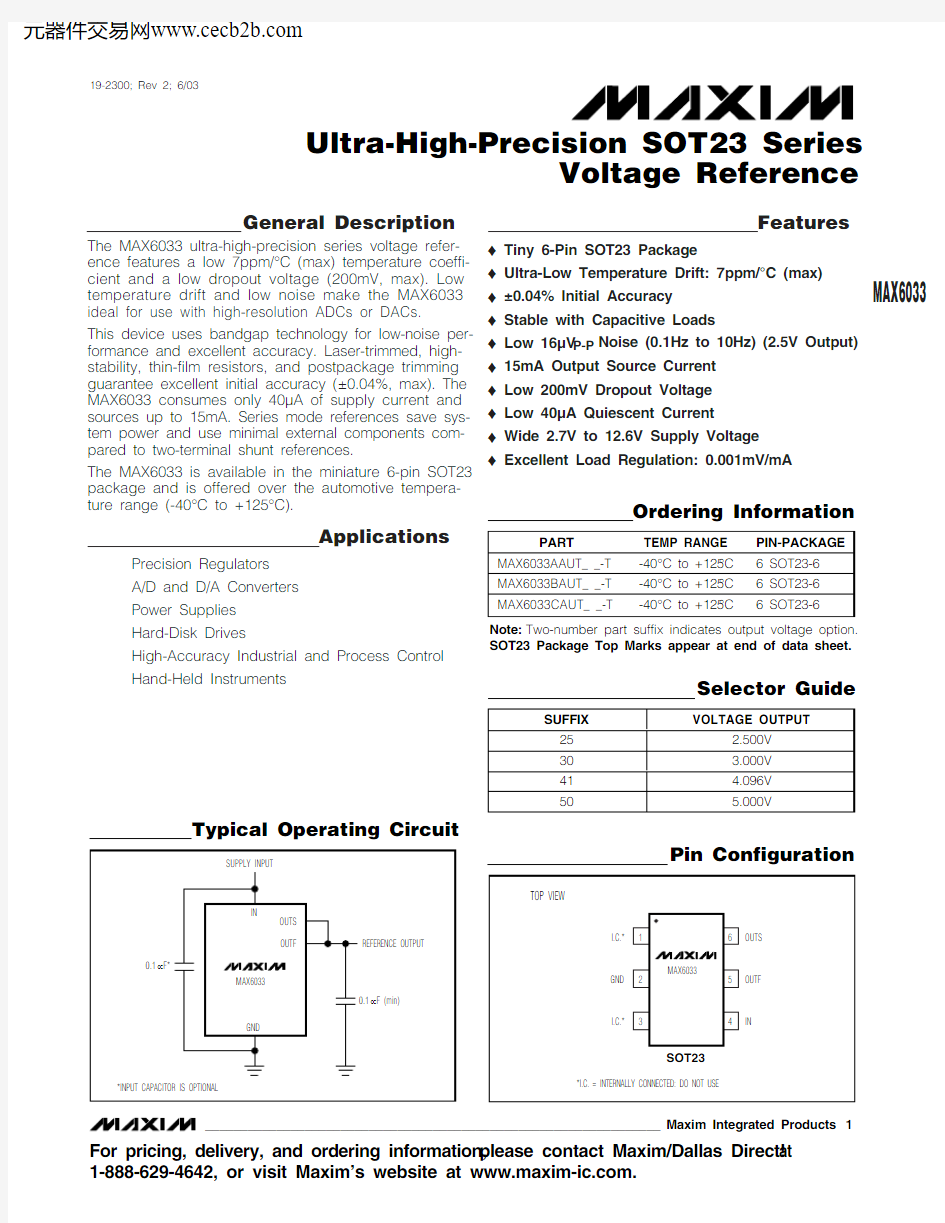
Typical Operating Circuit
19-2300; Rev 2; 6/03
For pricing, delivery, and ordering information,please contact Maxim/Dallas Direct!at 1-888-629-4642, or visit Maxim’s website at https://www.doczj.com/doc/46924930.html,.
Note:Two-number part suffix indicates output voltage option.SOT23 Package Top Marks appear at end of data sheet.
M A X 6033
Ultra-High-Precision SOT23 Series Voltage Reference
ABSOLUTE MAXIMUM RATINGS
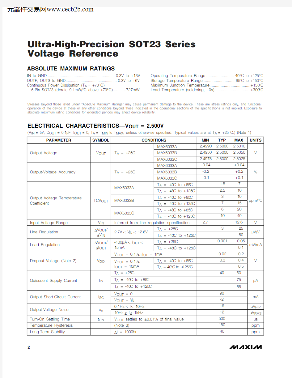
ELECTRICAL CHARACTERISTICS —V OUT = 2.500V
(V IN = 5V, C OUT = 0.1μF, I OUT = 0, T A = T MIN to T MAX , unless otherwise specified. Typical values are at T A = +25°C.) (Note 1)
Stresses beyond those listed under “Absolute Maximum Ratings” may cause permanent damage to the device. These are stress ratings only, and functional operation of the device at these or any other conditions beyond those indicated in the operational sections of the specifications is not implied. Exposure to absolute maximum rating conditions for extended periods may affect device reliability.
IN to GND...............................................................-0.3V to +13V OUTF, OUTS to GND................................................-0.3V to +6V Continuous Power Dissipation (T A = +70°C)
6-Pin SOT23 (derate 9.1mW/°C above +70°C)............727mW
Operating Temperature Range .........................-40°C to +125°C Storage Temperature Range.............................-65°C to +150°C Maximum Junction Temperature.....................................+150°C Lead Temperature (soldering, 10s).................................+300°C
MAX6033
Ultra-High-Precision SOT23 Series
Voltage Reference
_______________________________________________________________________________________3
ELECTRICAL CHARACTERISTICS —V OUT = 3.000V
(V IN = 5V, C OUT = 0.1μF, I OUT = 0, T A = T MIN to T MAX , unless otherwise specified. Typical values are at T A = +25°C.) (Note 1)
ELECTRICAL CHARACTERISTICS —V OUT = 4.096V
M A X 6033
Ultra-High-Precision SOT23 Series Voltage Reference
ELECTRICAL CHARACTERISTICS —V OUT = 4.096V (continued)
(V IN = 5V, C OUT = 0.1μF, I OUT = 0, T A = T MIN to T MAX , unless otherwise specified. Typical values are at T A = +25°C.) (Note 1)
ELECTRICAL CHARACTERISTICS —V OUT = 5.000V
(V = 5.5V, C = 0.1μF, I = 0, T = T to T , unless otherwise specified. Typical values are at T = +25°C.) (Note 1)
MAX6033
Ultra-High-Precision SOT23 Series
Voltage Reference
_______________________________________________________________________________________5
ELECTRICAL CHARACTERISTICS —V OUT = 5.000V (continued)
Typical Operating Characteristics
(V IN = 5V, C OUT = 0.1μF, I OUT = 0, T A = +25°C, unless otherwise specified.) (Note 4)
Note 2:Dropout Voltage is the minimum input voltage at which V OUT changes ≤0.1% from V OUT at V IN = 5V (V IN = 5.5V for
V OUT = 5V).
Note 3:Temperature Hysteresis is defined as the change in +25°C output voltage before and after cycling the device
from T MAX to T MIN .
OUTPUT VOLTAGE vs.TEMPERATURE (V OUT = 2.5V)
TEMPERATURE (°C)
O U T P U T V O L
T A G E (V )
110956580-105203550-252.49822.49842.49862.49882.49902.49922.49942.49962.49982.50002.50022.50042.50062.50082.50102.4980
-40125
OUTPUT VOLTAGE vs.TEMPERATURE (V OUT = 5V)
TEMPERATURE (°C)
O U T P U T V O L T A G E (V )
110956580-105203550-254.99824.99844.99864.99884.99904.99924.99944.99964.99985.00005.00025.00045.00065.00085.00104.9980
-40125
LOAD REGULATION (V OUT = 2.5V)
OUTPUT CURRENT (mA)
O U T P U T V O L T A G E (V )1816121424681002.49952.50002.50052.50102.50152.50202.50252.50302.50352.5040
2.4990
-220
M A X 6033
Ultra-High-Precision SOT23 Series Voltage Reference 6_______________________________________________________________________________________
Typical Operating Characteristics (continued)
(V IN = 5V, C OUT = 0.1μF, I OUT = 0, T A = +25°C, unless otherwise specified.) (Note 4)
LOAD REGULATION (V OUT = 5V)
OUTPUT CURRENT (mA)O U T P U T V O L T A G E (V )
18160
2
4
810126
144.9995.0005.0015.0025.0035.0045.0055.0064.998
-2
20
DROPOUT VOLTAGE vs. OUTPUT CURRENT
(V OUT = 2.5V)
OUTPUT CURRENT (mA)
D R O P O U T V O L T A G
E (m V )
181********
6
4
2
100200300400500600700
00
20
DROPOUT VOLTAGE vs. OUTPUT CURRENT
(V OUT = 5V)
OUTPUT CURRENT (mA)
D R O P O U T V O L T A G
E (m V )
181612144
6
8102
5010015020025030035040045050055060000
20
POWER-SUPPLY REJECTION RATIO vs. FREQUENCY (V OUT = 2.5V)
FREQUENCY (kHz)0.001
1
10
100
0.01
0.1
1000
P S R R (d B )
0-100
-90-80-70-60-50-40-10-20-30-100
-70-80-90
-60-50-40-30-20-1000.001
0.10.011101001000POWER-SUPPLY REJECTION RATIO vs. FREQUENCY (V OUT = 5V)
M A X 6033 t o c 08
FREQUENCY (kHz)
P S R R (d B )
SUPPLY CURRENT vs. INPUT VOLTAGE
(V OUT = 2.5V)
INPUT VOLTAGE (V)
S U P P L Y C U R R E N T (μA )
121191034567812153045607590105120135150
013
SUPPLY CURRENT vs. INPUT VOLTAGE
(V OUT = 5V)
INPUT VOLTAGE (V)
S U P P L Y C U R R E N T (μA )
12119103456781220406080100120140160180200220
013
0.1Hz TO 10Hz OUTPUT NOISE
(V OUT = 2.5V)
MAX6033 toc11
V OUT 4μV/div 1s/div 0.1Hz TO 10Hz OUTPUT NOISE
(V OUT = 5V)
MAX6033 toc12
V OUT 10μV/div
1s/div
MAX6033
Ultra-High-Precision SOT23 Series
Voltage Reference
_______________________________________________________________________________________7
LOAD TRANSIENT (V OUT = 2.5V)
2.5V
10mA
I OUT
10mA/div
V OUT 50mV/div AC-COUPLED
400μs/div
V IN = 5V C OUT = 0.1μF
LOAD TRANSIENT (V OUT = 2.5V)
2.5V
-100μA
1mA 1ms/div
I OUT 1mA/div
V OUT 50mV/div AC-COUPLED
V IN = 5V C OUT = 0.1μF
LOAD TRANSIENT (V OUT = 2.5V)
MAX6033 toc15
2.5V
10mA
I OUT
10mA/div
V OUT 50mV/div AC-COUPLED
400μs/div
V IN = 5V C OUT = 10μF
LOAD TRANSIENT (V OUT = 2.5V)
MAX6033 toc16
2.5V
-100μA
1mA
I OUT 1mA/div
V OUT 20mV/div AC-COUPLED
1ms/div
V IN = 5V C OUT = 10μF
LINE TRANSIENT (V OUT = 2.5V)
MAX6033 toc17
5.5V
2.5V
4.5V V
OUT 10mV/div AC-COUPLED
V IN
500mV/div AC-COUPLED
400μs/div C OUT = 0.1μF
LINE TRANSIENT (V OUT
= 5V)
6.5V
5V
5.5V
V OUT 10mV/div AC-COUPLED
V IN
500mV/div AC-COUPLED
1ms/div
Typical Operating Characteristics (continued)
(V IN = 5V, C OUT = 0.1μF, I OUT = 0, T A = +25°C, unless otherwise specified.) (Note 4)
M A X 6033
Ultra-High-Precision SOT23 Series Voltage Reference 8_______________________________________________________________________________________
Typical Operating Characteristics (continued)
(V IN = 5V, C OUT = 0.1μF, I OUT = 0, T A = +25°C, unless otherwise specified.) (Note 4)
TURN-ON TRANSIENT (V OUT = 2.5V)
5V
2.5V
V OUT 1V/div
V IN 2V/div
100μs/div
0C OUT = 0.1μF
TURN-ON TRANSIENT
(V OUT = 5V)
MAX6033 toc20
5.5V
5V
V OUT 2V/div
V IN 2V/div
400μs/div
C OUT = 0.1μF
TURN-ON TRANSIENT (V OUT = 2.5V)
5V
2.5V
V OUT 1V/div
V IN 2V/div
2ms/div
C OUT = 10μF
TURN-ON TRANSIENT
(V OUT = 5V)
5.5V
5V
V OUT 2V/div
V IN 2V/div
2ms/div
C OUT = 10μF
Note 4:Many of the MAX6033 Typical Operating Characteristics are similar. The extremes of these characteristics are found in the
MAX6033 (2.5V output) and the MAX6033 (5V output). The Typical Operating Characteristics of the remainder of the MAX6033 family typically lie between these two extremes and can be estimated based on their output voltages.
LONG-TERM STABILITY vs. TIME
(V OUT = 2.5V)
TIME (HOURS)
V O U T (V )
9008006007002003004005001002.499952.50000
2.500052.500102.500152.500202.50025
2.500302.500352.50040
2.49990
01000
LONG-TERM STABILITY vs. TIME
(V OUT
= 5V)
TIME (HOURS)
V O U T (V )
9008006007002003004005001005.00005.00015.00025.00035.00045.00055.00065.00075.00085.0009
4.9999
01000
Applications Information
Bypassing/Load Capacitance
For the best line-transient performance, decouple the input with a 0.1μF ceramic capacitor as shown in the Typical Operating Circuit . Place the capacitor as close to I N as possible. When transient performance is less important, no capacitor is necessary.
The MAX6033 family requires a minimum output capac-itance of 0.1μF for stability and is stable with capacitive loads (including the bypass capacitance) of up to 100μF. In applications where the load or the supply can experience step changes, a larger output capacitor reduces the amount of overshoot (undershoot) and improves the circuit ’s transient response. Place output capacitors as close to the device as possible.
Supply Current
The quiescent supply current of the MAX6033 series reference is typically 40μA and is virtually independent of the supply voltage. In the MAX6033 family, the load current is drawn from the input only when required, so supply current is not wasted and efficiency is maxi-mized at all input voltages. This improved efficiency reduces power dissipation and extends battery life.
When the supply voltage is below the minimum-speci-fied input voltage (as during turn-on), the devices can draw up to 150μA beyond the nominal supply current.The input voltage source must be capable of providing this current to ensure reliable turn-on.
Output-Voltage Hysteresis
Output voltage hysteresis is the change in the output voltage at T A = +25°C before and after the device is cycled over its entire operating temperature range.Hysteresis is caused by differential package stress appearing across the bandgap core transistors. The typical temperature hysteresis value is 150ppm.
Turn-On Time
These devices typically turn on and settle to within 0.01% of their final value in >1μs. The turn-on time can increase up to 2ms with the device operating at the minimum dropout voltage and the maximum load.
Precision Current Source
Figure 1 shows a typical circuit providing a precision current source. The OUTF output provides the bias cur-rent for the bipolar transistor. OUTS senses the voltage across the resistor and adjusts the current sourced by OUTF accordingly.
High-Resolution DAC and Reference from Single Supply
Figure 2 shows a typical circuit providing both the power supply and reference for a high-resolution DAC.A MAX6033 with 2.5V output provides the reference voltage for the DAC.
MAX6033
Ultra-High-Precision SOT23 Series
Voltage Reference
_______________________________________________________________________________________9
Figure 1. Precision Current Source
M A X 6033
Ultra-High-Precision SOT23 Series Voltage Reference 10______________________________________________________________________________________
Chip Information
TRANSISTOR COUNT: 656PROCESS: BiCMOS
SOT23 Package Top Marks
MAX6033
Ultra-High-Precision SOT23 Series
Voltage Reference
Maxim cannot assume responsibility for use of any circuitry other than circuitry entirely embod ied in a Maxim prod uct. No circuit patent licenses are implied. Maxim reserves the right to change the circuitry and specifications without notice at any time.
Maxim Integrated Products, 120 San Gabriel Drive, Sunnyvale, CA 94086 408-737-7600 ____________________11?2003 Maxim Integrated Products
Printed USA
is a registered trademark of Maxim Integrated Products.
Package Information
(The package drawing(s) in this data sheet may not reflect the most current specifications. For the latest package outline information go to https://www.doczj.com/doc/46924930.html,/packages .)